paper - IEEE Xplore
paper - IEEE Xplore
paper - IEEE Xplore

Create successful ePaper yourself
Turn your PDF publications into a flip-book with our unique Google optimized e-Paper software.
1512 <strong>IEEE</strong> TRANSACTIONS ON CIRCUITS AND SYSTEMS—I: REGULAR PAPERS, VOL. 58, NO. 7, JULY 2011<br />
II. CYCLIC VERNIER TIME-TO-DIGITAL CONVERTER<br />
A. TDC Architecture<br />
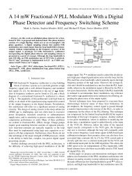
Fig. 2 shows the block diagram of a cyclic Vernier TDC [6],<br />
[7]. The goal of the TDC is to measure the time difference between<br />
the rising edges of the “Start” and “Stop” signals, which<br />
are and in the ADPLL, respectively. When the “Start”<br />
is asserted, the slow DCO starts to oscillate with a period of<br />
, and the number of oscillations is counted by the coarse<br />
counter. After an input delay of , the “Stop” signal is asserted<br />
which triggers the faster DCO to oscillate with a period<br />
of . At this time, the coarse counter is disabled, and the output<br />
of the counter represents a coarse measurement of the time between<br />
“Start” and “Stop” rising-edges . To improve the<br />
measurement accuracy, the residue of the input delay is<br />
measured by the Vernier structure. When is slightly smaller<br />
than , the time difference between rising edges of the two<br />
oscillations is reduced every cycle by the difference in periods<br />
, and the edge of the fast DCO eventually catches up<br />
to the slow DCO. By counting the number of cycles it takes for<br />
the fast DCO to catch up with the slow DCO, is measured.<br />
Then, the overall measurement of can be determined as<br />
follows:<br />
Fig. 2. (a) Block diagram of the proposed TDC and (b) timing diagram.<br />
(1)<br />
(2)<br />
where and are the number of cycles of the slow and fast<br />
oscillations, respectively, and is programmed to be<br />
much smaller than . As shown in Fig. 2, the TDC operates in<br />
two-steps; a coarse step and a fine step. The coarse step resolution<br />
is the period of the slow DCO, and the fine step resolution<br />
is the difference between the periods of the two DCOs. Note that<br />
the fine resolution does not depend on the absolute frequencies<br />
of the DCOs, but only their difference in periods. This is crucial<br />
for the calibration of mismatch between the P&R-ed DCOs<br />
discussed in Section III.<br />
Unlike conventional Vernier delay lines, the cyclic Vernier<br />
TDC adopts the ring structure to extend input range, limited only<br />
by the counter size that easily scales according to the application.<br />
Also, the linearity of the TDC improves by utilizing the periods<br />
of the DCOs, which is repetitive and consistent over operation,<br />
while the delay per stage in Vernier delay lines is more susceptible<br />
to variation and mismatch. One drawback of the cyclic<br />
Vernier TDC is a large latency of the fine step measurement. It<br />
takes one period of the fast DCO cycle to resolve a time<br />
difference of one fine step resolution . To reduce the<br />
conversion time, we adopt the two-step operation. The coarse<br />
step covers a large input time difference without any latency,<br />
and the residue of the coarse step is measured by the fine step,<br />
which is less than one cycle of the slow DCO. Also, this fine step<br />
range can be further reduced by the edge detector described in<br />
Section II-C.<br />
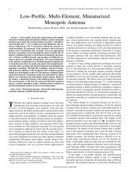
B. Digitally Controlled Oscillator<br />
While the previous cyclic Vernier TDC architectures [6],<br />
[7] adopt voltage controlled oscillators (VCOs), which require<br />
custom design and layout, the proposed TDC adopts DCOs<br />
Fig. 3. Digitally controlled oscillator with tristate buffers. The buffers from<br />
standard cell library are automatically placed-and-routed.<br />
that are implemented with only standard cells and P&R-ed.<br />
Fig. 3 shows the structure of the DCO. The DCO consists of<br />
three stages, and each stage is implemented with eight parallel<br />
inverting tristate buffers which are digitally controlled. Tristate<br />
buffers are available in commercial standard cell libraries.<br />
While the load capacitance at each stage is fixed by the number<br />
of buffers and wiring capacitance, the driving strength can<br />
be varied by turning on a different number of tristate buffers,<br />
thereby configuring the frequency of the DCO. Since the buffers<br />
are automatically P&R-ed by design tools, the placement and<br />
routing of the buffers are not regular as illustrated in Fig. 3.<br />
This results in systematic mismatch in the wiring capacitance,<br />
and thus a unique effective drive strength for each buffer.<br />
Though the individual drive strength cannot be controlled in<br />
the automated layout, the placement area and the wire lengths<br />
are constrained by layout algorithms, and statistics of the P&R<br />
mismatch is, to some extent, predictable at the design phase.<br />
In the proposed TDC, both the slow and fast DCOs are<br />
identically designed in a Verilog description, and automatically<br />
P&R-ed. Then, the P&R mismatch is characterized in the<br />
calibration mode, and the DCOs are configured to have slightly<br />
different periods, utilizing the P&R mismatch. The P&R mismatch<br />
provides higher resolution for the TDC, compared to<br />
the resolution obtained when the buffers are ideally matched.
![[Sample B: Approval/Signature Sheet]](https://img.yumpu.com/34084789/1/190x245/sample-b-approval-signature-sheet.jpg?quality=85)