R4300i Product Information - MIPS Technologies, Inc.
R4300i Product Information - MIPS Technologies, Inc.
R4300i Product Information - MIPS Technologies, Inc.

Create successful ePaper yourself
Turn your PDF publications into a flip-book with our unique Google optimized e-Paper software.
<strong>R4300i</strong> MICROPROCESSOR<br />
PRODUCT INFORMATION<br />
mips<br />
Open RISC Technology<br />
<strong>R4300i</strong> MICROPROCESSOR<br />
Description<br />
The <strong>R4300i</strong> is a low-cost RISC microprocessor optimized for demanding consumer applications. The <strong>R4300i</strong> provides<br />
performance equivalent to a high-end PC at a cost point to enable set-top terminals, games and portable consumer devices.<br />
The <strong>R4300i</strong> is compatible with the <strong>MIPS</strong> R4000 family of RISC microprocessors and will run all existing <strong>MIPS</strong> software.<br />
Unlike its predecessors designed for use in workstations, the <strong>R4300i</strong> is expected to lower the cost of systems in which it is<br />
used, a requirement for price-sensitive consumer products. The <strong>R4300i</strong> is also an effective embedded processor, supported<br />
by currently available development tools and providing very high performance at a low price-point.<br />
Features<br />
Low Power Dissipation:<br />
• 1.8W (normal)<br />
High Performance at 100MHz:<br />
• 60 SPECint92<br />
• 45 SPECfp92<br />
High bandwidth interface:<br />
• Max throughput 250MB/s<br />
• 32-bit address/data bus<br />
• 4-deep flush buffers<br />
High integration on-chip:<br />
• 16K I-cache, 8K D-cache<br />
• Unified datapath<br />
• 32 double-entry J-TLB<br />
• 2 entry micro I-TLB<br />
Power Management Features:<br />
• Reduced Power Mode<br />
• Instant On/Off<br />
R4000 family compatibility:<br />
• R4000 software compatible<br />
• Runs Windows NT/UNIX<br />
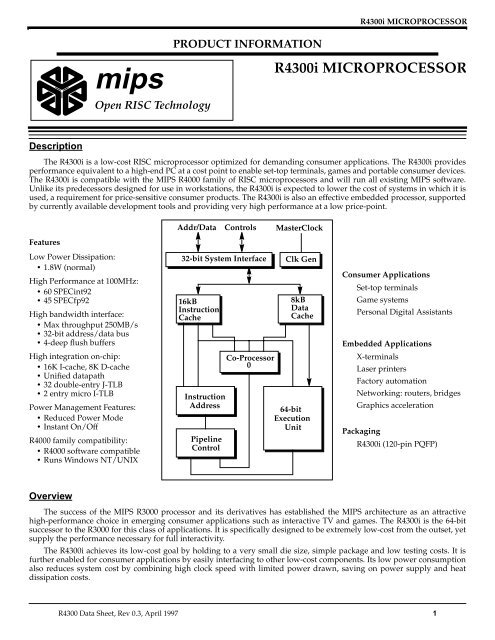
Addr/Data<br />
Controls<br />
32-bit System Interface<br />
16kB<br />
Instruction<br />
Cache<br />
Instruction<br />
Address<br />
Pipeline<br />
Control<br />
Co-Processor<br />
0<br />
MasterClock<br />
Clk Gen<br />
8kB<br />
Data<br />
Cache<br />
64-bit<br />
Execution<br />
Unit<br />
Consumer Applications<br />
Set-top terminals<br />
Game systems<br />
Personal Digital Assistants<br />
Embedded Applications<br />
X-terminals<br />
Laser printers<br />
Factory automation<br />
Networking: routers, bridges<br />
Graphics acceleration<br />
Packaging<br />
<strong>R4300i</strong> (120-pin PQFP)<br />
Overview<br />
The success of the <strong>MIPS</strong> R3000 processor and its derivatives has established the <strong>MIPS</strong> architecture as an attractive<br />
high-performance choice in emerging consumer applications such as interactive TV and games. The <strong>R4300i</strong> is the 64-bit<br />
successor to the R3000 for this class of applications. It is specifically designed to be extremely low-cost from the outset, yet<br />
supply the performance necessary for full interactivity.<br />
The <strong>R4300i</strong> achieves its low-cost goal by holding to a very small die size, simple package and low testing costs. It is<br />
further enabled for consumer applications by easily interfacing to other low-cost components. Its low power consumption<br />
also reduces system cost by combining high clock speed with limited power drawn, saving on power supply and heat<br />
dissipation costs.<br />
R4300 Data Sheet, Rev 0.3, April 1997 1
<strong>R4300i</strong> MICROPROCESSOR<br />
Overview (cont.)<br />
The <strong>R4300i</strong> has a number of design features to reduce<br />
power. These include an all-dynamic design, unified integer<br />
and floating-point datapath, a reduced power mode of<br />
operation, and caches partitioned into separate banks.<br />
Printers, networking devices and other embedded<br />
applications will also benefit from the high performance,<br />
low cost and high-bandwidth interface of the <strong>R4300i</strong>. The<br />
<strong>R4300i</strong> is the next standard in low-cost processing in the<br />
<strong>MIPS</strong> Microprocessor family.<br />
<strong>R4300i</strong> Architecture<br />
Data Format<br />
The <strong>R4300i</strong> defines a 64-bit double-word, a 32-bit word,<br />
a 16-bit halfword and an 8-bit byte. The byte ordering is<br />
configurable in either Big-endian or Little-endian format.<br />
Figures 1 and 2 show the ordering of bytes for Big-endian<br />
and Little-endian conventions<br />
.<br />
High<br />
Addr<br />
Low<br />
Addr<br />
High<br />
Addr<br />
Low<br />
Addr<br />
31 24 23 16 15 8 7 0<br />
byte-C byte-D byte-E byte-F<br />
byte-8 byte-9 byte-A byte-B<br />
byte-4 byte-5 byte-6 byte-7<br />
byte-0 byte-1 byte-2 byte-3<br />
Figure 1 Big-endian Byte Alignment<br />
Figure 2 Little-endian Byte Alignment<br />
Word<br />
Address<br />
C<br />
8<br />
4<br />
0<br />
Most significant byte is at lowest address<br />
Word is addressed by byte address of most significant byte<br />
31 24 23 16 15 8 7 0<br />
byte-F byte-E byte-D byte-C<br />
byte-B byte-A byte-9 byte-8<br />
byte-7 byte-6 byte-5 byte-4<br />
byte-3 byte-2 byte-1 byte-0<br />
Word<br />
Address<br />
C<br />
8<br />
4<br />
0<br />
Least significant byte is at lowest address<br />
Word is addressed by byte address of least significant byte<br />
Processor Resources<br />
The <strong>R4300i</strong> CPU provides sixty-four 64-bit wide<br />
registers. Thirty-two of these registers, referred to as<br />
General Purpose Register (GPRs), are reserved for integer<br />
operations while the other thirty-two register, referred to as<br />
Floating Point General Purpose Register (FGRs), are<br />
reserved for floating point operations. These two register<br />
sets are shown in Figure 3.<br />
General Purpose Regs (GPRs)<br />
63 32 31 0<br />
r0<br />
r1<br />
r2<br />
r30<br />
r31<br />
FP General Purpose Regs (FGRs)<br />
63 32 31 0<br />
FGR0<br />
FGR1<br />
FGR2<br />
Figure 3 General Purpose Registers<br />
The width of these registers depends on the mode of<br />
operation. In 32-bit mode, they are treated as 32 bits wide.<br />
In 64-bit mode, they are treated as 64 bits wide.<br />
The <strong>R4300i</strong> also contains six special registers: the<br />
program counter (PC), multiply/divide result Hi and Lo,<br />
Load/Link (LL) bit, and floating point Implementation and<br />
Control registers FCR0 and FCR31; shown in Figure 4. The<br />
program counter register contains the address of the<br />
current instruction. The multiply/divide registers store the<br />
result of integer multiply operations and the quotient and<br />
remainder of integer divide operations. The load/link bit is<br />
dedicated for load-link and store-conditional instructions<br />
which can be used to perform SYNC operations. The two<br />
floating point control registers, FCR0 and FCR31, provide<br />
the implementation/revision information and<br />
control/status of the floating point coprocessor (CP1).<br />
Program Counter (PC)<br />
63<br />
32 31<br />
PC<br />
Multiply/Divide Registers<br />
63<br />
32 31<br />
MultHI<br />
MultLO<br />
0<br />
0<br />
Floating Point<br />
Impl/Rev<br />
Control/Status<br />
Registers<br />
Figure 4 Special Registers<br />
FGR30<br />
FGR31<br />
In addition, the <strong>R4300i</strong> operates with up to three<br />
tightly coupled coprocessors (designated CP0 through<br />
CP2). Coprocessor zero (CP0) is implemented as an<br />
integral part of the CPU and supports the virtual memory<br />
system together with exception handling. Coprocessor one<br />
(CP1) is reserved for the floating point unit, while<br />
coprocessor two is reserved for future use.<br />
Coprocessor zero contains registers shown in Figure 5<br />
plus a 32-entry TLB with each entry consisting of an<br />
even/odd pair of physical addresses and tag field.<br />
31<br />
FCR0<br />
FCR31<br />
LLbit<br />
0<br />
0<br />
2 R4300 Data Sheet, Rev 0.3, April 1997
<strong>R4300i</strong> MICROPROCESSOR<br />
.<br />
EntryHi<br />
10*<br />
EVEN<br />
ENTRIES<br />
Config<br />
16*<br />
EntryLo0 2*<br />
EntryLo1 3*<br />
ODD<br />
ENTRIES<br />
Safe Entries Safe Entries<br />
PRId<br />
15*<br />
PageMask<br />
5*<br />
Index<br />
0*<br />
Random<br />
1*<br />
Wired<br />
6*<br />
Context<br />
4*<br />
XContext<br />
20*<br />
BadVAddr<br />
8*<br />
LLAddr<br />
17*<br />
TagHi<br />
29*<br />
WatchHi<br />
19*<br />
Count<br />
9*<br />
Figure 5 Coprocessor-0 Registers<br />
The CP0 registers can be considered as two distinct<br />
functional sets. The first set comprises those which support<br />
the TLB operations. The second set is formed from those<br />
registers that reflect the status of the processor. All of the<br />
CP0 registers are accessible by software.<br />
Instruction Set<br />
All <strong>R4300i</strong> instructions are 32 bits (single word) long<br />
aligned on word boundaries, as shown in Figure 6.<br />
I-Type (Immediate)<br />
31<br />
26 25<br />
21 20<br />
Op code rs rt<br />
31<br />
6<br />
J-Type (Jump)<br />
Op code<br />
6<br />
26 25<br />
5<br />
5<br />
16 15<br />
target<br />
26<br />
SR<br />
12*<br />
CacheErr<br />
27*<br />
EPC<br />
14*<br />
Immediate<br />
16<br />
CP0<br />
REGISTERS<br />
TagLo<br />
28*<br />
WatchLo<br />
18*<br />
Compare<br />
11*<br />
Cause<br />
13*<br />
PErr<br />
26*<br />
ErrEPC<br />
30*<br />
0<br />
0<br />
This approach simplifies instruction decoding. More<br />
complicated operations and addressing modes are<br />
synthesized by the compiler. There are three instruction<br />
formats: I-type (immediate), J-type (jump), and R-type<br />
(register).<br />
Load and Store instructions move data between<br />
memory and the general registers. They are all immediate<br />
(I-type) instructions. The only addressing mode that load<br />
and store instructions directly support is base register plus<br />
16-bit signed extended immediate offset.<br />
Load and store instruction opcodes determine the<br />
access type which indicates the size of the data item to be<br />
loaded or stored. Regardless of the access type or<br />
byte-numbering order (endianness), the address field<br />
specifies the lowest byte of the address location being<br />
accessed.<br />
Computational instructions perform arithmetic,<br />
logical, shift, multiply, and divide operations on values in<br />
registers. They occur in both register (R-Type) format, in<br />
which both operands are registers, and immediate (I-Type)<br />
format, in which one operand is a 16-bit immediate. When<br />
operating in 64-bit mode, 32-bit operands must be correctly<br />
sign extended.<br />
Jump and branch instructions change the control flow of<br />
a program. They occur in both register (R-Type) format, and<br />
immediate (I-Type) format. All jump and branch<br />
instructions occur with an architecture delay of one<br />
instruction; that is, the instruction immediately following<br />
the jump or branch is always executed while the target<br />
instruction is being fetched.<br />
Special instructions allow the software to initiate traps<br />
and are always R-Type.<br />
Exception instructions offer a trapping mechanism to<br />
assist in software debug.<br />
Coprocessor instructions perform operations in the<br />
respective coprocessors. Coprocessor loads and stores are<br />
I-type, and coprocessor computational instructions have<br />
coprocessor dependent formats.<br />
R-Type (Register)<br />
31<br />
26 25<br />
21 20<br />
Op code rs rt<br />
6<br />
Op code<br />
rs<br />
rt<br />
immediate<br />
target<br />
rd<br />
sa<br />
funct<br />
5<br />
5<br />
16 15<br />
5<br />
11 10<br />
5<br />
6 5<br />
rd sa funct<br />
is a 6-bit operation code<br />
is a 5-bit source register specifier<br />
is a 5-bit target register specifier<br />
is a 16-bit immediate, branch displacement or<br />
address displacement<br />
is a 26-bit jump target address<br />
is a 5-bit destination register specifier<br />
is a 5-bit shift amount<br />
is a 5-bit function field<br />
6<br />
0<br />
Pipeline<br />
The <strong>R4300i</strong> processor has a five-stage execution<br />
pipeline, as shown in Figure 7. Each pipeline stage takes<br />
one pclock to execute. The frequency of pclock can be either<br />
1, 1.5, 2, or 3 times the frequency of the MasterClock,<br />
depending on the state of DivMode 1:0 signals. The<br />
execution of each instruction thus has a latency of at least<br />
five pcycles. Once the pipeline has been completely filled,<br />
five instructions are always being executed simultaneously.<br />
When the pipeline is not stalled, the processor has a<br />
throughput of one instruction per pcycle. The pipeline is<br />
in-order issue, in-order execution, and in-order completion,<br />
the same order as in the instruction stream.<br />
Figure 6 Instruction Formats<br />
3 R4300 Data Sheet, Rev 0.3, April 1997
<strong>R4300i</strong> MICROPROCESSOR<br />
PClock<br />
Phase<br />
Cycle<br />
Instr. Fetch<br />
Instr. Decode<br />
Reg. File Read<br />
Arithmetic/Logical<br />
Operations<br />
Load/Store<br />
Operations<br />
Jump/Branch<br />
Operations<br />
Φ1 Φ2 Φ1 Φ2 Φ1 Φ2 Φ1 Φ2 Φ1 Φ2<br />
IC RF EX DC WB<br />
ITLB<br />
ICF<br />
ITC<br />
IDEC<br />
RFR<br />
Figure 7 Pipeline Activities<br />
The five stages of the <strong>R4300i</strong> pipeline are: Instruction<br />
Cache (IC), Instruction Decode and Register File Read (RF),<br />
Execution (EX), Data Cache Read (DC), and Register File or<br />
Data Cache Write Back (WB). Figure 7 shows the activities<br />
occurring during each pipeline stage for ALU, load and<br />
store, and branch instructions. Below are detail descriptions<br />
of the activities during each stage.<br />
IC: An instruction address is presented by the<br />
address unit and the instruction cache fetch<br />
begins. The instruction micro-TLB starts the<br />
virtual-to-physical address translation.<br />
RF: The instruction becomes available and the<br />
instruction decoder decodes the instruction and<br />
checks for interlock conditions. The instruction<br />
cache tag is checked against the page frame<br />
number obtained from the micro-TLB. Any<br />
required operands are read from the register file<br />
and the result from the EX or DC stages is<br />
bypassed to the following EX stage if required.<br />
The address unit generates the next instruction<br />
address.<br />
ALU<br />
BCMP<br />
IVA<br />
DVA<br />
Cycle Phase Mnemonic Descriptions<br />
IC<br />
RF<br />
EX<br />
DC<br />
WB<br />
Φ1<br />
Φ2<br />
ICF<br />
ITLB<br />
No activity<br />
RFW<br />
DTLB DTC<br />
DCR LA RFW<br />
Instruction Cache Fetch<br />
Instruction micro-TLB read<br />
Φ1 ITC Instruction cache Tag Check<br />
Φ2<br />
Φ1<br />
Φ2<br />
Φ1<br />
Φ2<br />
Φ1<br />
Φ2<br />
RFR<br />
IDEC<br />
IVA<br />
BCMP<br />
ALU<br />
DVA<br />
DCR<br />
DTLB<br />
LA<br />
DTC<br />
DCW<br />
RFW<br />
DCW<br />
Register File Read<br />
Instruction Decode<br />
Instruction Virtual Address Calculation<br />
Branch Compare<br />
Arithmetic Logic Operation<br />
Data Virtual Address Calculation<br />
No new activity started<br />
Data Cache Read<br />
Data TLB look-up<br />
Load Data Alignment<br />
Data Cache Tag Check<br />
Data Cache Write<br />
Register File Write<br />
No activity<br />
EX: For ALU class instructions, the ALU performs an<br />
arithmetic or logical operation. For load and<br />
store class instructions, the ALU generates the<br />
data virtual address. For branch instructions, the<br />
ALU determines whether the branch condition is<br />
true.<br />
DC: For load and store instructions, the data cache is<br />
accessed and data virtual-to-physical address<br />
translation is performed. At the end of the DC<br />
stage, the data becomes available and the<br />
load-align shifts the data to a word or<br />
double-word boundary. In addition, the data<br />
cache tag is checked against the page frame<br />
number obtained from the joint TLB.<br />
WB: For register-to-register or load instructions, the<br />
result is written back to the register file. For store<br />
instructions, the data cache is updated with the<br />
store data.<br />
The <strong>R4300i</strong> has a branch delay of one cycle and a load<br />
delay of one cycle. The branch delay is observed by noting<br />
that the branch compare logic operates during the EX<br />
pipestage, producing the target address which is available<br />
for the IC pipestage of the second subsequent instruction.<br />
The first subsequent instruction is the instruction in the<br />
delay slot and will be allowed to complete whether the<br />
branch is taken or not, as illustrated in Figure 8.<br />
Figure 8 Branch Delay Slot<br />
Similarly, the load delay of one is evident when the<br />
completion of a load at the end of the DC pipeline stage<br />
produces an operand which is available for the EX<br />
pipestage of the second subsequent instruction. The load<br />
delay is illustrated in Figure 9.<br />
.<br />
beq r2, r3, target<br />
ld r2, (r4)<br />
addi r4, 4<br />
addi r2, 1<br />
IC RF EX DC WB<br />
target: ld r4, (r5)<br />
IC RF EX DC WB<br />
add r2, r6<br />
IC RF EX DC WB<br />
IC RF EX DC WB<br />
IC RF EX DC WB<br />
load instruction<br />
IC RF EX DC WB<br />
Figure 9 Load Delay Slot<br />
branch instruction<br />
load delay slot<br />
branch delay slot<br />
instruction<br />
target<br />
instruction<br />
load data is bypassed<br />
from DC to EX pipestage<br />
Hardware detects whether the instruction in the branch<br />
delay slot is dependent on the register to be loaded, and<br />
interlocks accordingly.<br />
The pipeline flow is interrupted when an interlock<br />
condition is detected or when an exception occurs. An<br />
interlock condition is resolved by stalling the whole<br />
4 R4300 Data Sheet, Rev 0.3, April 1997
<strong>R4300i</strong> MICROPROCESSOR<br />
pipeline. On the other hand an exception aborts the relevant<br />
instruction and all those that follow.<br />
Figure 10 illustrates the various interlock conditions<br />
and the different types of exceptions, at their pre-defined<br />
pipeline stages.<br />
The execution unit is tightly coupled to the on-chip<br />
cache memory system, instruction and data caches, and the<br />
on-chip memory management unit, CP0. This unit has a<br />
multifunction pipe and is responsible for the execution of:<br />
• Integer arithmetic and logic instructions<br />
• Floating-point Coprocessor CP1 instructions<br />
PClock<br />
Phase<br />
Cycle<br />
Stalls<br />
Exceptions<br />
Φ1 Φ2 Φ1 Φ2 Φ1 Φ2 Φ1 Φ2 Φ1 Φ2<br />
IC RF EX DC WB<br />
ITM<br />
ICB<br />
IADE<br />
ITLB<br />
IBE<br />
LDI<br />
MCI<br />
CPI<br />
SYSC<br />
BRPT<br />
CPU<br />
RSVD<br />
DCM<br />
DCB<br />
COp<br />
RST<br />
NMI<br />
OVFL<br />
TRAP<br />
FPE<br />
CPE<br />
DAE<br />
DTLB<br />
WAT<br />
DBE<br />
INTR<br />
CP0I<br />
Pipe Interlock Conditions<br />
Descriptions<br />
Descriptions<br />
ITM Instruction TLB Miss ICB Instruction Cache Busy<br />
LDI Load Interlock MCI Multi-Cycle Interlock<br />
CPI Coprocessor-2 Interlock DCB Data Cache Busy<br />
COp Cache Op DCM Data Cache Miss<br />
CP0I CP0 Bypass Interlock<br />
Pipe Exception Conditions<br />
Descriptions<br />
Descriptions<br />
IADE Instruction Address Error OVFL Integer Overflow<br />
ITLB Instruction TLB Miss TRAP TRAP Exception<br />
IBE Instruction Bus Error FPE Floating Point Exception<br />
SYSC System Call Instruction CPE Coprocessor-2 Exception<br />
CPU Coprocessor Unusable DAE Data Address Error<br />
RSVD Reserved Instruction DTLB Data TLB Exception<br />
RST External Reset Exception DBE Data Bus Error<br />
NMI Non-Maskable Interrupt INTR External Interrupt<br />
BRPT BreakPoint Instruction WAT Reference Watch Address<br />
Figure 10 Pipeline Interlocks and Exceptions<br />
In the case of simultaneous stall requests from different<br />
pipestages, the pipeline control unit prioritizes which stall<br />
request is allowed to be resolved, in case of possible<br />
resource conflict. A stall request from the DC pipestage has<br />
higher priority than a stall request from the RF pipestage.<br />
Execution Unit<br />
The execution unit is designed to reduce power<br />
consumption and simplify the hardware requirements<br />
while providing a high level of performance by maximizing<br />
usage of each functional element. Integer performance is<br />
optimized for the <strong>R4300i</strong>’s target applications.<br />
• Branch/Jump instructions<br />
• Load/Store instructions<br />
• Exception instructions<br />
• Special instructions<br />
All floating-point instructions, as defined in the <strong>MIPS</strong><br />
ISA for the floating-point coprocessor CP1, are processed by<br />
the same hardware as used for the integer instructions.<br />
However, the execution of floating-point instructions can<br />
still be disabled via the “Coprocessor Unusable” CU bit<br />
defined in the CP0 Status register.<br />
The execution unit uses a modular design approach to<br />
further reduce dynamic power consumption. Control logic<br />
is partitioned into small independent blocks responsible for<br />
a set of instructions. When relevant instructions are not in<br />
the instruction stream, the corresponding control blocks<br />
become inactive. Also, when functional elements in the<br />
datapath are idle, they operate on a constant (0’s or 1’s)<br />
selected to minimize power dissipation.<br />
The execution unit’s datapath consists of: a 64-bit<br />
integer/mantissa datapath, an operand bypass network, 32<br />
64-bit integer registers, 32 64-bit floating-point registers, a<br />
12-bit exponent datapath, and a 64-bit instruction virtual<br />
address generator.<br />
As shown in Figure 11, the integer/mantissa datapath<br />
is 64 bits wide and is compatible with both 32-bit and 64-bit<br />
operands for integer and floating-point numbers. It has a<br />
Boolean Logic functional unit, a Carry-Propagate Adder, a<br />
CSA Multiplier, and a bi-directional Shifter.<br />
The Logical Operation unit performs all integer logical<br />
operations. The carry-propagated adder is used for all other<br />
integer and floating-point computational instructions. The<br />
adder is also used to compute data virtual address for load<br />
and store instructions, and to compare two operands in trap<br />
instructions. The CSA multiplier is used for both integer<br />
and floating-point multiplication, in single or double<br />
precision. The shifter is responsible for integer variable<br />
shifts, store align shifts, and floating-point<br />
post-normalization. It also has build-in<br />
guard/round/sticky collection logic for floating-point<br />
pre-alignment shift. In addition, the datapath has a Leading<br />
Zero Counter for floating-point normalization shift<br />
calculation, and a floating-point unpacker and repacker.<br />
5 R4300 Data Sheet, Rev 0.3, April 1997
<strong>R4300i</strong> MICROPROCESSOR<br />
BYPASS NETWORK<br />
COMBINED REGISTER FILE<br />
RS<br />
RT<br />
IMMEDIATE<br />
BYPASS MUX<br />
SIGN EXTEND<br />
UNPACK<br />
BYPASS MUX<br />
SIGN EXTEND<br />
UNPACK<br />
SIGN EXTEND<br />
SHIFT MUX<br />
SHIFT MUX<br />
SHIFT MUX<br />
OPMUX<br />
CSA<br />
MULTIPLIER<br />
BLOCK<br />
X<br />
Y<br />
CARRY-PROPAGATE ADDER<br />
Z<br />
SHIFTER<br />
LOGICAL<br />
OPERATION<br />
RESULT MUX<br />
RMUX<br />
SUM REG<br />
SIGN EXTEND<br />
REPACK<br />
DBUS<br />
LOAD ALIGNER<br />
WB REG<br />
DVA1DC<br />
Figure 11 Integer/Mantissa Datapath<br />
EXPONENTS FROM<br />
UNPACKER<br />
SR1 UnpExpS<br />
UnpExpT<br />
0 1<br />
FEEDBACK MUX<br />
Leading Zero Cnt<br />
Constant Gen<br />
ES MUX<br />
ET MUX<br />
S<br />
T<br />
CARRY-SELECT ADDER<br />
Cin=1 Cin=0<br />
RESULT MUX<br />
Result Check<br />
EXP SUM REG<br />
TO REPACK LOGIC<br />
Underflow<br />
Overflow<br />
One<br />
Zero<br />
> One<br />
Convert Limit Chk<br />
Figure 12 Exponent Datapath<br />
R4300 Data Sheet, Rev 0.3, April 1997 6
<strong>R4300i</strong> MICROPROCESSOR<br />
For load and store class instructions, the datapath can<br />
handle partial-words in either big- or little-endian mode.<br />
For store instructions, the main bi-directional shifter<br />
performs an alignment shift on the register read data. No<br />
concatenation of register read data with the original<br />
memory data is necessary since the data cache has byte<br />
write enable controls. For load instructions, it is necessary to<br />
maintain a load delay of one pclock cycle. Due to the timing<br />
requirements imposed by this load delay, a dedicated<br />
byte-wide shifter (Load Aligner) is needed to shift the<br />
memory read data in bytes, halfwords, and words in the<br />
right or left direction.<br />
The operand bypass network is built into the datapath<br />
to allow feedback of results from the EX and DC pipeline<br />
stages to the instructions in the following EX pipestage<br />
waiting to use the results as source operands rs and/or rt.<br />
This allows the following instruction to proceed without<br />
having to wait for the results to be written back to the<br />
register file. Similarly, to maintain the minimum branch<br />
delay slot of one pipeline clock cycle for all branch<br />
instructions on the floating-point condition, the results from<br />
the preceding floating-point compare instruction in the EX,<br />
DC, or WB pipestage will be fed back for branch condition<br />
testing in the RF pipestage.<br />
The exponent datapath is 12 bits wide. The twelfth bit<br />
(MSB) is used as both sign bit and overflow bit. The<br />
exponent datapath consists of a feedback mux and 2<br />
operand muxes to select the inputs from the adder, constant<br />
generating logic, a carry select adder, random logic to<br />
perform exception detection, and a register to hold the<br />
selected result from the adder, as shown in Figure 12.<br />
The inputs to the exponent unit come from the unpack<br />
logic, where the exponents are extracted from single- or<br />
double-precision floating-point operands. The<br />
carry-selected adder performs exponent subtraction,<br />
pre-alignment shift calculation, and exponent addition for<br />
post-normalization final update. The result is sent to the<br />
repack logic to be merged with the mantissa.<br />
The result of the exponent logic is compared with<br />
constants or ranges to check for various conditions by the<br />
result checker. These conditions include: underflow,<br />
overflow in single-precision number, overflow in<br />
double-precision number, one, zero, and convert limit<br />
check. The checks are performed as soon as data is available<br />
from the carry-select adder.<br />
The instruction virtual address unit is responsible for<br />
the generation of 64-bit instruction virtual addresses to be<br />
used by the micro-TLB, I-Cache and CP0. It has its own<br />
incrementor to calculate the next sequential address. It also<br />
has an equality comparator and a separate ripple-carry<br />
adder to generate the branch target address.<br />
In addition, the address unit has exception vector<br />
generator logic to decode the type of exception and then<br />
present the appropriate vector as the next PC address. It<br />
also has the exception PC register pipe chain to maintain a<br />
history of PC addresses for each pipestage so that the PC<br />
address associated with the exception causing instruction<br />
can be loaded into the Exception Program Counter (EPC)<br />
register.<br />
Cache Organization<br />
To achieve high performance, increase memory access<br />
bandwidth and reduce the latency of load and store<br />
instructions, the <strong>R4300i</strong> processor incorporates on-chip<br />
instruction and data caches. Each cache has its own 64-bit<br />
datapath and can be accessed in parallel with the other<br />
cache. Both the instruction and data caches are direct<br />
mapped, virtually indexed, and use physical tags. The<br />
<strong>R4300i</strong> cache organization is shown in Figure 13.<br />
D-Cache<br />
SysAD Output Data Path<br />
PAD Ring<br />
Flush-Buffer<br />
DBus<br />
32<br />
Data-Path/<br />
Control<br />
DTAG ITAG<br />
Cache<br />
Cntl<br />
SysAD Bus<br />
SysAD Input<br />
Data Path<br />
IBus<br />
Figure 13 <strong>R4300i</strong> Cache Organization<br />
The instruction cache is 16 kilobytes in size. It is<br />
organized as eight-word (32-byte) lines with a 21-bit tag<br />
entry associated with each line. The tag entry consists of a<br />
valid bit (V), and a 20-bit physical tag (bit 31:12 of the<br />
physical address). The format of an instruction cache line is<br />
shown in Figure 14.<br />
20 19<br />
V<br />
1<br />
Physical TAG<br />
20<br />
where:<br />
V<br />
PTAG<br />
Data<br />
Figure 14 <strong>R4300i</strong> Instruction Cache Line Form<br />
64<br />
64 64<br />
0<br />
31<br />
Data<br />
Data<br />
Data<br />
Data<br />
Data<br />
Data<br />
Data<br />
Data<br />
32<br />
I-Cache<br />
Valid bit<br />
20 bit physical tag (bit 31:12 of the physical address)<br />
Data word<br />
0<br />
7 R4300 Data Sheet, Rev 0.3, April 1997
<strong>R4300i</strong> MICROPROCESSOR<br />
An instruction cache line has two possible cache states:<br />
Invalid and Valid. A cache line with invalid cache state does<br />
not contain valid information. A cache line in a valid state<br />
contains valid information.<br />
The instruction cache is accessible in one p-cycle.<br />
Access begins on phase 2 of the IC pipestage and completes<br />
at the end of phase 1 of the RF pipestage. Each access will<br />
fetch two instructions. Therefore instruction fetching is<br />
required only on every other run cycle or when there is a<br />
jump/branch instruction in the EX pipestage. When there is<br />
a miss detected during an instruction cache access, a<br />
memory block read will be initiated from the system<br />
interface to replace the current cache line with the desired<br />
line.<br />
The data cache is 8 kilobytes in size. It is organized as<br />
four-word (16-byte) lines with a 22-bit tag entry associated<br />
with each line.The tag entry consists of a valid bit (V), a<br />
dirty bit (D), and a 20 bit physical tag (bit 31:12 of the<br />
physical address). The format of a data cache line is shown<br />
in Figure 15.<br />
21 20 19<br />
V D Physical TAG<br />
1 1<br />
21<br />
0<br />
Figure 15 <strong>R4300i</strong> Data Cache Line Format<br />
A data cache line has three possible cache states:<br />
invalid, valid clean, and valid dirty. A data cache line with<br />
an invalid state does not contain valid information. A cache<br />
line in valid clean state contains valid information and is<br />
consistent with main memory. A cache line in valid dirty<br />
state contains valid data but is not consistent with main<br />
memory. Figure 16 illustrates the data cache state transition<br />
sequence.<br />
Read Hit,<br />
Store.<br />
where:<br />
V<br />
D<br />
PTAG<br />
Data<br />
Figure 16 <strong>R4300i</strong> Data Cache State Transition<br />
The data cache uses a write-back cache policy. This<br />
means that store data is written to the cache line rather than<br />
31<br />
Data<br />
Data<br />
Data<br />
Data<br />
Valid bit<br />
Dirty Bit<br />
20 bit physical tag (bits 31:12 of the physical address)<br />
Data word<br />
Valid<br />
Dirty<br />
Cache-op<br />
Store<br />
Invalid<br />
Store<br />
Cache-op<br />
Read Miss<br />
Read<br />
32<br />
Cache-op<br />
Valid<br />
Clean<br />
0<br />
Read<br />
main memory. The modified cache line will be written back<br />
to main memory only when it needs to be replaced. For load<br />
or store misses, a cache block read will be issued to main<br />
memory to bring in a new line and the missed line will be<br />
handled in the following manner:<br />
Data load miss:<br />
• If the missed line is not dirty, it will be replaced<br />
with the new line.<br />
• If the missed line is dirty, the missed line will be<br />
moved to the flush-buffer, the new line will<br />
replaced the missed line, and the data in the<br />
flush-buffer will be written back to main memory.<br />
Data store miss:<br />
• If the missed line is not dirty, it will be replaced<br />
with the new line.<br />
• If the missed line is dirty, the missed line will be<br />
moved to the flush-buffer, the new line will be<br />
written to the cache, and the data in the<br />
flush-buffer will be written back to main memory.<br />
• In either store miss case, the store data is merged<br />
with the new line.<br />
The data cache is accessible on reads in one p-cycle. The<br />
access begins on phase 1 of the DC pipestage and completes<br />
at the end of phase 2 of the DC pipestage. Each access will<br />
fetch a double word. The data cache writes, however,<br />
execute in two p-cycles. A cache read is initiated in the first<br />
p-cycle, and a cache write with dirty bit set is initiated in the<br />
second p-cycle.<br />
The data cache can be accessed for byte, half-word,<br />
three-byte, word, five-byte, six-byte, seven-byte, and<br />
double-word. The data size of a partial load is derived from<br />
the access type from the integer control unit and the lower<br />
three address bits. The data alignment is performed by the<br />
datapath load aligner.<br />
To reduce the cache miss penalty, the address of the<br />
block read request will point to the location of the desired<br />
double-word. Since the data cache has a two double-word<br />
line size, the system interface will return the critical<br />
double-word first, followed by the remaining double-word.<br />
The return data will be written to the cache as it is put on the<br />
data bus to be used by the execution unit.<br />
The <strong>R4300i</strong> processor provides a variety of cache<br />
operations for use in maintaining the state and contents of<br />
the instruction and data caches. During the execution of the<br />
cache operation instructions, the processor may issue<br />
processor block read or write request to fill or write-back a<br />
cache line.<br />
Flush Buffer<br />
The <strong>R4300i</strong> Microprocessor contains a 4-entry on-chip<br />
flush buffer. The buffer is used as temporary data storage<br />
for outgoing data and is organized as a 4 deep fifo; that is it<br />
can buffer 4 addresses along with 4 double-words of data.<br />
For uncached write operations, the flush buffer can accept<br />
8 R4300 Data Sheet, Rev 0.3, April 1997
<strong>R4300i</strong> MICROPROCESSOR<br />
any combination of single or double-word data until it is<br />
full, with each write occupying one entry in the buffer. For<br />
data cache block write operations, the flush buffer accepts 2<br />
double-words with 1 address, occupying two entries in the<br />
buffer. It is able to take two block references at a time.<br />
Instruction cache block writes use 4 doublewords with 1<br />
address. Instruction cache block writes occupy the entire<br />
flush buffer. The flush buffer is able to take one read<br />
memory reference at a time.<br />
Address is a 32-bit physical address, and size indicates<br />
the size of data to be transferred out.<br />
During an uncached store, data will be stored in this<br />
buffer until it is taken by the external interface. While data<br />
awaits in this area, processor pipeline continues to execute.<br />
During a load miss or a store miss to a cache line in the<br />
dirty state, a read request for the missing cache line is sent<br />
to the external interface. The dirty data is then stored in the<br />
flush buffer until the requested data is returned from the<br />
external interface. The processor pipeline continues to run<br />
while the flush buffer writes the dirty data to the external<br />
interface.<br />
If the flush buffer is full and the processor attempts a<br />
load or a store which requires external resources, the<br />
processor pipeline will stall until the buffer is emptied.<br />
Figure 17 shows the layout of the flush buffer.<br />
decode signals from the integer unit and interprets them to<br />
determine whether a CP0 register is to be read or written. It<br />
generates control signals for reading and writing TLB and<br />
ITLB entries.<br />
IVA<br />
DVA<br />
DBUS<br />
CACHE DATA<br />
INTERRUPTS<br />
INDEX<br />
ENHI<br />
ENLO<br />
ITLB<br />
TLB<br />
CP0REG<br />
TLBMISS<br />
ADDR CHK<br />
TAG<br />
DATA<br />
CP0CTL<br />
I-PFN<br />
D-PFN<br />
EXCEPTIONS<br />
STATUS<br />
Figure 18 <strong>R4300i</strong> Coprocessor 0 Block Diagram<br />
R/W Size Address Data<br />
1 4 32 64<br />
where:<br />
R/W Read/Write<br />
Size Transfer Size Field<br />
Address Flush Buffer Address<br />
Data Flush Buffer Data<br />
Figure 17 Flush Buffer Format<br />
Coprocessor 0<br />
The <strong>R4300i</strong> Coprocessor-0 functional unit performs two<br />
major functions. The first is memory management for the<br />
processor, and the second is exception processing. CP0 is<br />
logically divided into four subunits: CP0 Register Files<br />
(Cp0reg), Translation Look-aside Buffer (TLB), Instruction<br />
TLB (ITLB), and CP0 Control Unit (Cp0ctl). Figure 18 shows<br />
how these subunits interact with each other and other<br />
functional units.<br />
The CP0 registers consist of two functionally distinct<br />
sets. The first set comprises those that support the TLB<br />
operations, and the second set is formed from those<br />
registers that reflect the state of the processor. All of the CP0<br />
registers are readable by software. All but the Random,<br />
BadVAddr, PrId, and MskId registers are writable by<br />
software. The definitions of the CP0 registers are described<br />
in a later section.<br />
The CP0ctl subunit controls data transfer to and from<br />
the TLB, ITLB and CP0 registers. It takes the instruction<br />
In addition, the CP0ctl handles exception processing. Its<br />
function is to communicate with the pipeline control unit<br />
for interrupt signalling, and notification of TLB exceptions.<br />
It also performs address checking with regard to the type of<br />
instruction being executed, and various state bits in the<br />
Status register. For example, a User mode process may try to<br />
access a kernel data address. In this case, a Data Address<br />
Error exception would be detected, since the address<br />
Region bits would conflict with the KSU bits in the Status<br />
register.<br />
The Translation Look-aside Buffers (micro-TLB and<br />
joint TLB) are responsible for the translation of both<br />
instruction and data virtual addresses into physical<br />
addresses. The physical address is needed by the cache for<br />
its tag checks, and by the system interface for off-chip<br />
memory access, and various CP0 registers. The jTLB<br />
translates the lower 40 bits of the 64-bit virtual address size<br />
defined in the <strong>MIPS</strong>-III architecture, and provides a 32-bit<br />
physical address.<br />
The joint TLB contains 32 entries, each of which is<br />
simultaneously checked for a match with the extended<br />
virtual address. Each TLB entry maps an even-odd pair of<br />
pages. The page size is 4K, 16K, 64K, 256K, 1M, 4M or 16M<br />
bytes, which is specified on a per-entry basis by the MASK<br />
bit-mask field of the entry. The valid values of the MASK<br />
field and the effect on the translation is documented in the<br />
description of the PageMask register.<br />
A virtual address matches a TLB entry when the virtual<br />
page number (VPN) field of the virtual address equals the<br />
VPN field of the TLB entry, and either the Global (G) bit of<br />
9 R4300 Data Sheet, Rev 0.3, April 1997
<strong>R4300i</strong> MICROPROCESSOR<br />
the TLB entry is set or the address space identifier (ASID)<br />
field of the virtual address (as held in the EntryHi register)<br />
matches the ASID field of the TLB entry. Although the valid<br />
(V) bit of the entry must be set for a valid translation to take<br />
place, it is not involved in the determination of a matching<br />
TLB entry.<br />
The operation of the TLB is not defined if more than one<br />
entry in the TLB matches. If one TLB entry matches, the<br />
physical address and access control bits (N, D, and V) are<br />
retrieved; otherwise a TLB refill exception occurs. If the<br />
access control bits (D and V) indicate that the access is not<br />
valid, a TLB modification or TLB invalid exception occurs.<br />
The format of a TLB entry in 32-bit addressing mode is<br />
shown in Figure 19.<br />
127 121 120 109 108 96<br />
- MASK<br />
-<br />
7<br />
12<br />
13<br />
95 77 76 75 72 71 64<br />
VPN2 G - ASID<br />
19<br />
1 4 8<br />
63 57 56 38 37 35 34 33 32<br />
- PFN (even) C D V -<br />
6<br />
19<br />
3 1 1 1<br />
31 25 24 6 5 3 2 1 0<br />
- PFN (odd) C D V -<br />
6<br />
19<br />
3 1 1 1<br />
Figure 19 TLB Entry Format in 32-bit Addressing Mode<br />
The format of a TLB entry in 64-bit mode is shown in<br />
Figure 20.<br />
255<br />
217 216 205 204 192<br />
- MASK -<br />
39 12 13<br />
191 190 189 168 167<br />
141 140 139 136 135 128<br />
R<br />
VPN2 G - ASID<br />
2 22 27 1 4 8<br />
127<br />
89 88<br />
70 69 67 66 65 64<br />
- PFN (even) C D V -<br />
38<br />
19<br />
3 1 1 1<br />
63<br />
25 24<br />
6 5 3 2 1 0<br />
- PFN (odd) C D V -<br />
38<br />
19<br />
3 1 1 1<br />
Where:<br />
R Is the Region used to match VAddr 63..62<br />
MASK is the comparison MASK<br />
VPN2 is the Virtual Page Number / 2<br />
G Global bit<br />
ASID Address Space Identifier<br />
PFN Physical Page Number (upper 20 bits of the physical address)<br />
C Cache Algorithm (011=cached; 010=uncached)<br />
D If set, page is writable<br />
V If set, entry is valid<br />
Figure 20 TLB Entry Format in 64-bit Addressing Mode<br />
The <strong>R4300i</strong> also implements a two entry micro-TLB that<br />
is dedicated for instruction address translation. This allows<br />
instruction address translation to be done simultaneously<br />
with data address translation. If there is a miss in the<br />
micro-TLB, the pipeline will stall while the new TLB entry<br />
is transferred from the joint TLB to the micro-TLB. The two<br />
entry micro-TLB entry is fully associative with a Least<br />
Recently Used replacement algorithm. Each micro-TLB<br />
entry maps to a 4K byte page size only.<br />
CP0 Registers<br />
Table 1 lists all CP0 registers used in the <strong>R4300i</strong>.<br />
Attempting to write any unused register is undefined and<br />
may have an unpredictable effect on the <strong>R4300i</strong> processor.<br />
Attempting to read any unused register is undefined and<br />
may result in unpredictable data.<br />
Table 1 System Control Coprocessor 0 Registers<br />
Num Mnemonic Descriptions<br />
0 Index Programmable pointer into TLB array<br />
1 Random Random pointer into TLB array<br />
2 EntryLo0 Low half of the TLB entry for even VPN<br />
3 EntryLo1 Low half of the TLB entry for odd VPN<br />
4 Context Pointer to kernel PTE table<br />
5 PageMask TLB page mask<br />
6 Wired Number of wire TLB entries<br />
7 ---- Unused<br />
8 BadVAddr Bad virtual address<br />
9 Count Timer count<br />
10 EntryHi High half of TLB entry<br />
11 Compare Timer compare<br />
12 SR Status register<br />
13 Cause Cause register<br />
14 EPC Exception program counter<br />
15 PRid Processor revision identifier<br />
16 Config Configuration register<br />
17 LLAddr Load linked address<br />
18 WatchLo Memory reference trap address lower bits<br />
19 WatchHi Memory reference trap address upper bits<br />
20 XContext Context register for <strong>MIPS</strong>-III addressing<br />
21-25 ---- Unused<br />
26 PErr Not Used<br />
27 CacheErr Not Used<br />
28 TagLo Cache tag register<br />
29 TagHi Cache tag register (Reserved)<br />
30 ErrorEPC Error exception program counter<br />
31 ---- Unused<br />
The Index register is a read/write register in which 6 bits<br />
specify an entry into the on-chip TLB. The high order bit<br />
indicates the success or failure of a TLBP operation. The<br />
TLB Index register is used to specify the entry in the TLB<br />
affected by the TLBR and TLBWI instructions. Figure 21<br />
shows the Index register format.<br />
31 30 6 5 0<br />
P<br />
0<br />
Index<br />
1<br />
25<br />
6<br />
where:<br />
P Result of last Probe operation. Set to 1 if last TLB Probe<br />
instruction was unsuccessful<br />
index Index to entry in TLB<br />
0 Must be all zeroes on reads and writes<br />
Figure 21 Index Register<br />
10 R4300 Data Sheet, Rev 0.3, April 1997
<strong>R4300i</strong> MICROPROCESSOR<br />
The Random register is a read-only register in which 6<br />
bits specify an entry in the on-chip TLB. This register will<br />
decrement on every instruction executed. The values range<br />
between a low value determined by the TLB Wired register,<br />
and an upper bound of TLBENTRIES-1. The TLB Random<br />
register is used to specify the entry in the TLB affected by<br />
the TLBWR instruction. Upon system reset, or when the<br />
Wired register is written, this register will be set to the upper<br />
limit. Figure 22 shows the Random register format.<br />
31 6 5 0<br />
0<br />
Random<br />
26<br />
6<br />
where:<br />
Random Index to entry in TLB<br />
0 Must be all zeroes on reads and writes<br />
Figure 22 CP0 Random Register<br />
The EntryLo0 and EntryLo1 registers are a read/write<br />
register pair that are used to access on-chip TLB. EntryLo0 is<br />
used for the even virtual pages while EntryLo1 is used for<br />
the odd virtual pages. They contain the Page Frame<br />
Number, along with several configuration bits for the TLB<br />
entry. They are used by the TLBR, TLBWI, and TLBWR<br />
instructions. Figure 23 shows the EntryLo0 and EntryLo1<br />
registers format.<br />
the base address of the PTE table of the current user address<br />
space. Figure 24 shows the Context register format.<br />
32 bit Mode:<br />
31 23 22<br />
4 3 0<br />
PTEBase<br />
BadVPN2<br />
0<br />
9<br />
19<br />
4<br />
64 bit Mode:<br />
63 23 22<br />
4 3 0<br />
PTEBase<br />
BadVPN2 0<br />
41<br />
19<br />
4<br />
where:<br />
PTEBase Base address of the Page Entry Table<br />
BadVPN2 Virtual Page Number of the failed virtual address<br />
divided by two<br />
0 Must be zero on reads and writes<br />
Figure 24 CP0 Context Register<br />
The PageMask register is a read/write register that is<br />
used when reading or writing an on-chip TLB. The TLBR,<br />
TLBWI, and TLBWR instructions use this register as a<br />
source or destination.When virtual addresses are presented<br />
for translation, the corresponding bits in the TLB specify<br />
which of virtual address bits 24.13 participate in the<br />
comparison. This implements a variable page size on a per<br />
entry basis. <strong>R4300i</strong> implements 4K, 16K, 64K, 256K, 1M, 4M<br />
and 16M pages. Figure 25 shows the PageMask register<br />
format.<br />
.<br />
32 bit Mode:<br />
31 30 29<br />
6 5 3 2 1 0<br />
0<br />
PFN<br />
C D V G<br />
2<br />
64 bit Mode:<br />
24<br />
3 1 1 1<br />
63 30 29<br />
6 5 3 2 1 0<br />
0<br />
PFN<br />
C D V G<br />
34<br />
24<br />
3 1 1 1<br />
where:<br />
PFN Physical Frame Number<br />
C Cache Algorithm. If C=011, then page is cached. If<br />
C=010, then it is uncached. All other values of C are<br />
cached.<br />
V Page Valid if 1, invalid if 0<br />
G If set in both Lo0 and Lo1, then ignore ASID<br />
0 Must be zero on all reads and writes<br />
D Page Dirty if 1, Clean if 0<br />
Figure 23 CP0 EntryLo0 and EntryLo1 Registers<br />
The Context register is a read/write register containing<br />
a pointer into a kernel Page Table Entry (PTE) array. It is<br />
designed for use in the TLB refill handler. The BadVPN2<br />
field is not writable. It contains the VPN of the most recently<br />
translated virtual address that did not have a valid<br />
translation. It contains bits 31:13 of the virtual address that<br />
caused the TLB miss. Bit 12 is excluded because a single TLB<br />
entry maps an even-odd page pair. This format can be used<br />
directly as an address for pages of size 4K bytes. For all<br />
other page sizes the value must be shifted and masked. The<br />
PTEBase field is writable as well as readable, and indicates<br />
31 25 24<br />
13 12<br />
0<br />
0<br />
MASK<br />
0<br />
7<br />
12<br />
13<br />
where:<br />
MASK Mask for Virtual Page Number. For <strong>R4300i</strong>, this is<br />
0000_0000_0000 for 4K pages, 0000_0000_0011 for 16K<br />
pages and so on up to 111111111111 for 16M pages.<br />
0 Must be zero on reads and writes<br />
Figure 25 CP0 Mask Register<br />
The TLB Wired register is a read/write register that<br />
specifies the boundary between the wired and random<br />
entries of the TLB. This register is set to 0 upon reset.<br />
Writing to this register also sets the Random register to 31.<br />
Writing a value greater than TLBENTRIES-1 to this register<br />
will result in undefined behavior. Figure 26 shows the Wired<br />
register.<br />
31 6 5 0<br />
0<br />
26<br />
Wired<br />
6<br />
where:<br />
Wired TLB wired boundary<br />
0 Must be zero on reads and writes<br />
Figure 26 CP0 Wired Register<br />
11 R4300 Data Sheet, Rev 0.3, April 1997
<strong>R4300i</strong> MICROPROCESSOR<br />
The Bad Virtual Address register is a read-only register<br />
that displays the most recently translated virtual address<br />
which failed to have a valid translation or which had an<br />
addressing error. Figure 27 shows the BadVAddr register<br />
format.<br />
The Compare register is a read/write register. When the<br />
value of the Count register equals the value of the Compare<br />
register, IP 7 of the Cause register is set. This causes an<br />
interrupt on the next execution cycle in which interrupt is<br />
enabled. Writing to the Compare register will clear the timer<br />
interrupt. Figure 30 shows the Compare register format.<br />
32 bit Mode:<br />
31 0<br />
BadVAddr<br />
32<br />
64 bit Mode:<br />
63 0<br />
BadVAddr<br />
64<br />
where:<br />
BadVAddr Most recently translated virtual address that failed to<br />
have a valid translation or that had an addressing<br />
error.<br />
Figure 27 CP0 BadVAddr Register<br />
The Count register is a read/write register used to<br />
implement timer services. It increments at a constant rate<br />
based on the clock cycle. On <strong>R4300i</strong>i, it will increment at<br />
one-half the PClock speed. When the Count register has<br />
reached all ones, it will roll over to all zeroes and continue<br />
counting. This register is both readable and writable. It is<br />
writable for diagnostic purposes. Figure 28 shows the Count<br />
register format.<br />
31 0<br />
where:<br />
Count<br />
Count<br />
Figure 28 CP0 Count Register<br />
The EntryHi register is a read/write register that is used<br />
to access on-chip TLB. It is used by the TLBR, TLBWI, and<br />
TLBWR instructions. EntryHi contains the Address Space<br />
Identifier (ASID) and the Virtual Page Number. Figure 29<br />
shows the EntryHi register format.<br />
32<br />
Current count value, updated at 1/2 Pclock Frequency<br />
32 bit Mode:<br />
31 13 12 8 7 0<br />
VPN2<br />
0 ASID<br />
19<br />
5 8<br />
64 bit Mode:<br />
63 62 61 40 39<br />
13 12 8 7 0<br />
R FILL<br />
VPN2<br />
0 ASID<br />
2 22<br />
27<br />
5 8<br />
where:<br />
R Region (00=user, 01=supervisor,11=kernel) used to<br />
match vAddr 63..62<br />
FILL Reserved; undefined on read, should be 0 or -1 on<br />
write (should sign extend the virtual page number)<br />
VPN2 Virtual Page Number divided by 2<br />
0 Must be zero on reads and writes<br />
ASID Address Space Identifier<br />
31 0<br />
where:<br />
Compare<br />
Compare<br />
32<br />
Value to be compared to Count register. An interrupt<br />
will be signaled when they are equal.<br />
Figure 30 CP0 Compare Registers<br />
The Status register is a read/write register that contains<br />
the various mode, enables, and status bits used on <strong>R4300i</strong>.<br />
The contents of this register are undefined after a reset,<br />
except for TS, which is zero; ERL and BEV, which are one;<br />
and RP, which is zero. The SR bit is 0 after a Cold Reset, and<br />
1 after NMI or (Soft) Reset. Figure 31 shows the Status<br />
register format.<br />
31 28 27 26 25 24 23 22 21 20 19 18 17 16<br />
CU RP FR RE ITS rsvd BEV TS SR 0 CH CE DE<br />
4 1 1 1 1 1 1 1 1 1 1 1 1<br />
15<br />
8 7 6 5 4 3 2 1 0<br />
IM<br />
KX SX UX KSU ERLEXL IE<br />
8<br />
1 1 1 2 1 1 1<br />
where:<br />
CU Coprocessor Unit usable if 1. CP0 is always usable by<br />
the kernel<br />
RP Reduced Power. Changes clock to quarter speed.<br />
FR If set, enables <strong>MIPS</strong> III additional floating point<br />
registers.<br />
RE Reverse Endian. Changes endianness in user mode.<br />
ITS Instruction Trace Support. Enables trace support.<br />
rsvd Reserved for future use.<br />
BEV Controls location of TLB refill and general exception<br />
vectors. (0=normal, 1= bootstrap).<br />
TS TLB Shutdown has occurred.<br />
SR Soft Reset or NMI has occurred.<br />
0 Must be zeroes on read and write.<br />
CH This is the CP0 Condition bit. It is readable and<br />
writable by software only. It is not set or cleared by<br />
hardware.<br />
CE, DE These fields are included to maintain compatibility.<br />
with the R4200 and are not used in the <strong>R4300i</strong>.<br />
IM Interrupt Mask. Enables and disables interrupts.<br />
KX Kernel extended addressing enabled.<br />
SX Supervisor extended addressing enabled.<br />
UX User extended addressing enabled.<br />
KSU Mode (10=user, 01=supervisor, 00=kernel)<br />
ERL Error Level. Normal when zero, error if one<br />
EXL Exception Level. Normal when zero, exception if one<br />
IE Interrupt Enable.<br />
Figure 31 CP0 Status Register<br />
Figure 29 CP0 EntryHi Register<br />
12 R4300 Data Sheet, Rev 0.3, April 1997
<strong>R4300i</strong> MICROPROCESSOR<br />
The Cause register is a read/write register that describes<br />
the nature of the last exception. A five-bit exception code<br />
indicates the cause of the exception and the remaining fields<br />
contain detailed information relevant to the handling of<br />
certain types of exceptions. The Branch Delay bit indicates<br />
whether the EPC has been adjusted to point at the branch<br />
instruction which precedes the next restartable instruction.<br />
The Coprocessor Error field indicates the unit number<br />
referenced by an instruction causing a “Coprocessor<br />
Unusable” exception. The Interrupt Pending field indicates<br />
which interrupts are pending. This field indicates the<br />
current status and changes in response to external signals.<br />
IP7 is the timer interrupt bit, set when the Count register<br />
equals the Compare register. IP6:2 are the external interrupts,<br />
set when the external interrupts are signalled. An external<br />
interrupt is set at one of the external interrupt pins or via a<br />
write request on the SysAD bus. IP1:0 are software<br />
interrupts, and may be written to set or clear software<br />
interrupts. Figure 32 shows the Cause register format.<br />
31 30 29 28 27<br />
16 15<br />
8 7 6 2 1 0<br />
BD 0 CE<br />
0<br />
IP 0 ExcCode 0<br />
1 1 2 12<br />
8 1 5 2<br />
where:<br />
BD Branch Delay<br />
CE Coprocessor Error<br />
IP Interrupt pending<br />
ExcCode Exception Code:<br />
0 Must be zeroes on read and write<br />
0 Int Interrupt<br />
1 Mod TLB modification exception<br />
2 TLBL TLB Exception (Load or instruction<br />
fetch)<br />
3 TLBS TLB Exception (Store)<br />
4 AdEL Address Error Exception (Load or<br />
instruction fetch)<br />
5 AdES Address Error Exception (Store)<br />
6 IBE Bus Error Exception (instruction<br />
fetch)<br />
7 DBE Bus Error Exception (data reference:<br />
load or store)<br />
8 Sys SysCall Exception<br />
9 Bp Breakpoint Exception<br />
10 RI Reserved instruction Exception<br />
11 CpU Coprocessor Unusable Exception<br />
12 Ov Arithmetic Overflow Exception<br />
13 Tr Trap Exception<br />
14 --- Reserved<br />
15 FPE Floating Point Exception<br />
16-22 Reserved<br />
23 Watch Reference to WatchHi/WatchLo<br />
address<br />
24-31 Reserved<br />
Figure 32 CP0 Cause Register<br />
The EPC register is a read/write register that contains<br />
the address at which instruction processing may resume<br />
after servicing an exception. For synchronous exceptions,<br />
the EPC register contains either the virtual address of the<br />
instruction which was the direct cause of the exception, or<br />
when that instruction is in a branch delay slot, the EPC<br />
contains the virtual address of the immediately preceding<br />
branch or jump instruction and the Branch Delay bit in the<br />
Cause register is set. If the exception is caused by<br />
recoverable, temporary conditions (such as a TLB miss), the<br />
EPC contains the virtual address of the instruction which<br />
caused the exception. Thus, after correcting the conditions,<br />
the EPC contains a point at which execution can be<br />
legitimately resumed. Figure 33 shows the format of EPC<br />
register.<br />
32 bit Mode:<br />
31 0<br />
EPC<br />
32<br />
64 bit Mode:<br />
63 0<br />
EPC<br />
64<br />
where:<br />
EPC Exception Program Counter.<br />
Figure 33 CP0 EPC Register<br />
The PRId register is a read-only register that contains<br />
information that identifies the implementation and revision<br />
level of the processor and associated system control<br />
coprocessor. The revision number can distinguish some<br />
chip revisions. However, <strong>MIPS</strong> is free to change this register<br />
at any time and does not guarantee that changes to its chips<br />
will necessarily change the revision number, or that changes<br />
to the revision number necessarily reflect real chip changes.<br />
For this reason, software should not rely on the revision<br />
number to characterize the chip. Figure 34 shows the<br />
Processor Revision Identifier register format.<br />
31 16 15<br />
8 7<br />
0<br />
0 Imp Rev<br />
16<br />
where:<br />
Imp Implementation identifier: 0x0B for <strong>R4300i</strong><br />
Rev Revision Number<br />
0 Returns zeroes on reads.<br />
Figure 34 CP0 Revision Identifier Register<br />
The Config register specifies various configuration<br />
options that are available for <strong>R4300i</strong>. It is compatible with<br />
the R4000 Config register, but only a small subset of the<br />
options available on the R4000 are possible on <strong>R4300i</strong>. For<br />
that reason, there are many fields which are set to constant<br />
values. The EP and BE fields are writable by software only.<br />
The CU and K0 fields are readable and writable by software.<br />
There is no other mechanism for writing to these fields, and<br />
their values are undefined after Reset. Figure 35 shows the<br />
Configuration register format.<br />
8<br />
8<br />
13 R4300 Data Sheet, Rev 0.3, April 1997
<strong>R4300i</strong> MICROPROCESSOR<br />
31 30 28 27 24 23 20 19 18 1716 15 14 13 12 11 9 8 6 5 4 3 2 0<br />
0 EC EP 0000 01 1 0<br />
B<br />
1 1 0 010 001 1 0 C K0<br />
E<br />
U<br />
4 4 4 2 1 1 1 1 1 1 3 3 1 1 1 3<br />
where:<br />
EC<br />
EP<br />
BE<br />
CU<br />
K0<br />
System Clock Ratio: Read only<br />
110 = 1:1<br />
111 = 1.5:1<br />
000 = 2:1<br />
001 = 3:1<br />
All other values of EC are undefined.<br />
Pattern for writeback data on SYSAD port<br />
0000 -> D<br />
0110 -> DxxDxx<br />
All other values of EP are undefined.<br />
BigEndianMem<br />
0 -> Memory and kernel are Little Endian<br />
1 -> Memory and kernel are Big Endian<br />
Reserved. (Read- and Writ-able by software)<br />
Kseg0 coherency algorithm. This has the same format<br />
as the C field in EntryLo0 and EntryLo1. The only<br />
defined values for K0 for <strong>R4300i</strong> are 010<br />
(noncacheable) and 011 (cacheable).<br />
0 Returns 0 on read.<br />
1 Returns 1 on read.<br />
Figure 35 CP0 Configuration Register<br />
The <strong>R4300i</strong>i processor provides a debugging feature to<br />
detect references to a physical address. Loads or stores to<br />
the location specified by the WatchHi/WatchLo register pair<br />
cause a Watch trap. Figure 36 shows WatchHi/WatchLo<br />
register formats.<br />
WatchLo:<br />
31 3 2 1 0<br />
PAddr<br />
0 R W<br />
29<br />
1 1 1<br />
WatchHi:<br />
31 4 3 0<br />
0<br />
PAddr<br />
31<br />
4<br />
where:<br />
PAddr Physical address<br />
WatchLo PAddr contains bits 31.3<br />
In the <strong>R4300i</strong> bits 3:0 of the WatchHi register<br />
are ignored but are software writable. This<br />
is to maintain compatibility with the R4000.<br />
R Trap on Read Access if 1<br />
W Trap on Write Access if 1<br />
0 Must be zeroes on reads and writes<br />
Figure 36 CP0 WatchLo and WatchHi Registers<br />
The LLAddr register contains the physical address read<br />
by the most recent Load Linked instruction. This register<br />
exists for diagnostic purposes, and serves no function<br />
during normal operation. It is both readable and writable by<br />
software. Figure 37 shows the LLAddr register format.<br />
31 0<br />
where:<br />
Paddr<br />
PAddr<br />
Bits 35..4 of the physical address. Note that for <strong>R4300i</strong>,<br />
the MSB of the physical address is only 31. A load<br />
linked instruction will write 0 into bits[31..29] of<br />
LLAddr, but a software write can set all 32 bits to any<br />
value. This maintains compatibility with R4000.<br />
Figure 37 CP0 LLAddr Register<br />
The XContext register is a read/write register<br />
containing a pointer into a kernel Page Table Entry (PTE)<br />
array. It is designed for use in the XTLB refill handler. The R<br />
and BadVPN2 fields are not writable. The register contains<br />
the VPN of the most recently translated virtual address that<br />
did not have a valid translation. It contains bits 39.13 of the<br />
virtual address that caused the TLB miss. Bit 12 is excluded<br />
because a single TLB entry maps an even-odd page pair.<br />
This format can be used directly as an address for pages of<br />
size 4K bytes. For all other page sizes this value must be<br />
shifted and masked. The PTEBase field is writable as well as<br />
readable, and indicates the base address of the PTE table of<br />
the current user address space. Figure 38 shows XContext<br />
register format.<br />
63 3332 31 30<br />
4 3 0<br />
PTEBase R BadVPN2 0<br />
31<br />
2<br />
27<br />
4<br />
where:<br />
PTEBase Base address of the Page Entry Table<br />
BadVPN2 Virtual Page Number of the failed virtual address<br />
divided by two<br />
R Region (00=user, 01=supervisor, 11=kernel)<br />
0 Must be zero on reads and writes<br />
Figure 38 CP0 XContext Register<br />
The PErr register, shown in Figure 39, is included only<br />
to maintain compatibility with the R4200. The <strong>R4300i</strong> does<br />
not implement parity, hence this register is not used by<br />
hardware. However, the register is software readable and<br />
writable.<br />
31 8 7 0<br />
0<br />
24<br />
Diagnostic<br />
8<br />
where:<br />
Diagnostic Eight bit diagnostic field<br />
0 Must be zeroes on all reads and writes<br />
Figure 39 CP0 PErr Register<br />
14 R4300 Data Sheet, Rev 0.3, April 1997
<strong>R4300i</strong> MICROPROCESSOR<br />
The CacheErr register, shown in Figure 40, is included<br />
only to maintain compatibility with the R4200. The <strong>R4300i</strong><br />
does not implement cache errors, hence this register is not<br />
used by hardware. It is a read only register which returns a<br />
zero value when read.<br />
31 0<br />
0<br />
Figure 40 CP0 CacheErr Register<br />
The TagLo register is a 32-bit read/write register used to<br />
hold the cache tag during cache initialization and<br />
diagnostics. The TagHi register is reserved for future use.<br />
These two Tag registers are written by the CACHE and<br />
MTC0 instructions. Figure 41 shows TagLo and TagHi<br />
register formats.<br />
TagLo:<br />
31 28 27<br />
8 7 65 0<br />
0 PTagLo PState 0<br />
4<br />
20<br />
2 6<br />
TagHi:<br />
31 0<br />
TagHi = 0<br />
32<br />
where:<br />
PTagLo Physical address bits 31.12<br />
Pstate Primary Cache State (0=invalid, 3=Dirty)<br />
0 Must be zeroes on reads and writes<br />
Figure 41 CP0 TagLo TagHi Registers<br />
32 bit Mode:<br />
31 0<br />
ErrorEPC<br />
64 bit Mode:<br />
32<br />
63 0<br />
Error EPC<br />
64<br />
ErrorEPC Exception Program Counter for Reset and NMI.<br />
Figure 42 CP0 ErrorEPC Register<br />
Memory Management<br />
The <strong>R4300i</strong> processor provides a full-featured memory<br />
management unit (MMU) which uses an on-chip<br />
translation look-aside buffer (TLB) to translate virtual<br />
address into physical address. The TLB is a fully associative<br />
memory that holds 32 entries, which provide mapping to 32<br />
odd/even pairs (64 pages). When address mapping is<br />
indicated, each TLB entry is checked simultaneously for a<br />
match with the virtual address that is extended with an<br />
ASID stored in the EntryHi register. The address is mapped<br />
to a page of size of between 4Kbytes and 16Mbytes.<br />
The processor virtual address can be either 32 or 64 bits<br />
wide, depending on whether the processor is operating in<br />
32-bit or 64-bit mode.<br />
• In 32-bit mode, addresses are 32 bits wide. The<br />
maximum user process size is 2 gigabytes (2 31 ).<br />
• In 64-bit mode, addresses are 64 bits wide. The<br />
maximum user process size is 1 terabyte (2 40 ).<br />
Figure 43 shows the translation of a virtual address into<br />
a physical address.<br />
The ErrorEPC register is similar to the EPC, but is used<br />
to store the PC on Reset and NMI exceptions. It is<br />
read/write register and contains the virtual address at<br />
which instruction processing may resume after servicing an<br />
Error or Reset/NMI exceptions.<br />
The EPC register contains either the virtual address of<br />
the instruction which was the direct cause of the exception,<br />
or when that instruction is in a branch delay slot, the EPC<br />
contains the virtual address of the immediately preceding<br />
branch or jump instruction. There is no branch delay slot<br />
indication for ErrorEPC. Figure 42 shows ErrorEPC register<br />
format.<br />
1. Virtual address (VA) represented<br />
by the virtual page number<br />
(VPN) is compared with tag in<br />
TLB.<br />
2. If there is a match, the page frame<br />
number (PFN) representing the<br />
upper bits of the physical<br />
address (PA) is output from the<br />
TLB.<br />
3. The Offset, which does not pass<br />
through the TLB, is then<br />
concatenated to the PFN.<br />
G<br />
TLB<br />
G<br />
Virtual address<br />
ASID VPN Offset<br />
ASID VPN<br />
EVEN PFN<br />
TLB<br />
Entry<br />
ODD PFN<br />
PFN<br />
Offset<br />
Physical address<br />
Figure 43 Virtual-to-Physical Address Translation<br />
15 R4300 Data Sheet, Rev 0.3, April 1997
<strong>R4300i</strong> MICROPROCESSOR<br />
Converting a virtual address to a physical address<br />
begins by comparing the virtual address from the processor<br />
with the virtual address in the TLB; there is a match when<br />
the virtual page number (VPN) of the address is the same as<br />
the VPN field of the entry, and either:<br />
• the Global (G) bit of the TLB entry is set, or<br />
• the ASID field of the virtual address is the same as<br />
the ASID field of the TLB entry.<br />
This match is referred to as a TLB hit. If there is no<br />
match, a TLB Miss exception is taken by the processor and<br />
software is allowed to refill the TLB from a page table of<br />
virtual/physical addresses in memory.<br />
If there is a virtual address match in the TLB, the<br />
physical address is output from the TLB and concatenated<br />
with the Offset, which represents an address within the page<br />
frame space.<br />
Figure 44 shows the virtual-to-physical address<br />
translation of a 32-bit mode address.<br />
39<br />
39<br />
ASID<br />
8<br />
Bits 31, 30 and 29 of the<br />
virtual address select user,<br />
supervisor, or kernel<br />
address spaces.<br />
Virtual Address with 1M (2 20 ) 4-Kbyte pages<br />
3231 2928 20 bits = 1M pages 12 11 0<br />
Virtual-to-physical<br />
translation in TLB<br />
TLB<br />
VPN<br />
Offset<br />
20 12<br />
Virtual-to-physical<br />
translation in TLB<br />
TLB<br />
32-bit Physical Address<br />
3231 2928 24 23 0<br />
ASID VPN<br />
Offset<br />
8<br />
8 24<br />
8 bits = 256 pages<br />
Virtual Address with 256 (2 8 )16-Mbyte pages<br />
Offset passed<br />
unchanged to<br />
physical<br />
memory<br />
31 0<br />
PFN<br />
Offset<br />
Offset passed<br />
unchanged to<br />
physical<br />
memory<br />
Figure 44 32-Bit-Mode Virtual Address Translation<br />
• The top portion of Figure 44 shows a virtual<br />
address with a 12-bit, or 4-Kbyte, page size,<br />
labelled Offset. The remaining 20 bits of the address<br />
represent the VPN, and index the 1M-entry page<br />
table.<br />
• The bottom portion of Figure 44 shows a virtual<br />
address with a 24-bit, or 16-Mbyte, page size,<br />
labelled Offset. The remaining 8 bits of the address<br />
represent the VPN, and index the 256-entry page<br />
table.<br />
Figure 45 shows the virtual-to-physical-address<br />
translation of a 64-bit mode address. This figure illustrates<br />
the two possible page sizes: a 4-Kbyte page (12 bits) and a<br />
16-Mbyte page (24 bits).<br />
• The top portion of Figure 45 shows a virtual<br />
address with a 12-bit, or 4-Kbyte, page size,<br />
labelled Offset. The remaining 28 bits of the address<br />
represent the VPN, and index the 256M-entry page<br />
table.<br />
• The bottom portion of Figure 45 shows a virtual<br />
address with a 24-bit, or 16-Mbyte, page size,<br />
labelled Offset. The remaining 16 bits of the<br />
address represent the VPN, and index the<br />
64K-entry page table.<br />
Mapped Virtual Address with 256M (2 28 ) 4-Kbyte pages<br />
71 64 63 62 61 40 39 28 bits = 256M pages 12 11 0<br />
ASID<br />
8<br />
VPN<br />
Offset<br />
71 64 63 62 61 40 39<br />
24 23 0<br />
ASID 0 or -1 VPN<br />
Offset<br />
8<br />
0 or -1<br />
24<br />
24 16<br />
24<br />
16 bits = 64K pages<br />
Virtual Address with 64K (2 16 )16-Mbyte pages<br />
28<br />
Virtual-to-physical<br />
TLB translation in TLB<br />
31 0<br />
PFN<br />
Offset<br />
TLB<br />
Virtual-to-physical<br />
translation in TLB<br />
Figure 45 64-Bit-Mode Virtual Address Translation<br />
The processor has three operating modes that function<br />
in both 32- and 64-bit operations: User mode, Supervisor<br />
mode, and Kernel mode. The address space for each mode<br />
of operation are described in the following sections.<br />
In User mode, a single, uniform virtual address<br />
space—labelled User segment—is available; its size is:<br />
• 2 Gbytes (2 31 bytes) in 32-bit mode (useg)<br />
• 1 Tbyte (2 40 bytes) in 64-bit mode (xuseg)<br />
The User segment starts at address 0 and the current<br />
active user process resides in either useg (in 32-bit mode) or<br />
xuseg (in 64-bit mode). The TLB identically maps all<br />
references to useg/xuseg from all modes, and controls cache<br />
accessibility * . Figure 46 shows User mode virtual address<br />
space.<br />
12<br />
32-bit Physical Address<br />
Offset passed<br />
unchanged to<br />
physical<br />
memory<br />
Offset passed<br />
unchanged<br />
physical memory<br />
* The cached (C) field in a TLB entry determines whether<br />
the reference is cached; see Figure 20.<br />
16 R4300 Data Sheet, Rev 0.3, April 1997
<strong>R4300i</strong> MICROPROCESSOR<br />
0x FFFF FFFF<br />
0x 8000 0000<br />
0x 0000 0000<br />
32-bit<br />
Address<br />
Error<br />
2 GB<br />
Mapped<br />
Figure 46 User Mode Virtual Address Space<br />
The processor operates in User mode when the Status<br />
register contains the following bit-values:<br />
• KSU bits = 10 2<br />
• EXL= 0<br />
• ERL= 0<br />
In conjunction with these bits, the UX bit in the Status<br />
register selects between 32- or 64-bit User mode addressing<br />
as follows:<br />
• when UX = 0, 32-bit useg space is selected<br />
• when UX = 1, 64-bit xuseg space is selected<br />
Supervisor mode is designed for layered operating<br />
systems in which a true kernel runs in <strong>R4300i</strong> Kernel mode,<br />
and the rest of the operating system runs in Supervisor<br />
mode. Figure 47 shows Supervisor mode address space.<br />
32-bit<br />
0x FFFF FFFF<br />
Address<br />
0x E000 0000 error<br />
0.5 GB<br />
0x C000 0000 Mapped<br />
Address<br />
0x A000 0000 error<br />
Address<br />
0x 8000 0000 error<br />
0x 0000 0000<br />
2 GB<br />
Mapped<br />
Figure 47 Supervisor Mode Virtual Address Space<br />
The processor operates in Supervisor mode when the<br />
Status register contains the following bit-values:<br />
• KSU= 01 2<br />
• EXL= 0<br />
• ERL= 0<br />
useg<br />
sseg<br />
suseg<br />
0x FFFF FFFF FFFF FFFF<br />
0x 0000 0100 0000 0000<br />
0x 0000 0000 0000 0000<br />
64-bit<br />
Address<br />
Error<br />
1 TB<br />
Mapped<br />
64-bit<br />
0x FFFF FFFF FFFF FFFF Address<br />
0x FFFF FFFF E000 0000<br />
error<br />
0.5 GB<br />
0x FFFF FFFF C000 0000<br />
Mapped<br />
Address<br />
0x 4000 0100 0000 0000 error<br />
1 TB<br />
Mapped<br />
0x 4000 0000 0000 0000<br />
Address<br />
0x 0000 0100 0000 0000 error<br />
1 TB<br />
Mapped<br />
0x 0000 0000 0000 0000<br />
xuseg<br />
csseg<br />
xsseg<br />
xsuseg<br />
In conjunction with these bits, the SX bit in the Status<br />
register selects between 32- or 64-bit Supervisor mode<br />
addressing:<br />
• when SX = 0, 32-bit supervisor space is selected<br />
• when SX = 1, 64-bit supervisor space is selected<br />
The processor operates in Kernel mode when the Status<br />
register contains one of the following values:<br />
• KSU= 00 2<br />
• EXL= 1<br />
• ERL= 1<br />
In conjunction with these bits, the KX bit in the Status<br />
register selects between 32- or 64-bit Kernel mode<br />
addressing:<br />
• when KX = 0, 32-bit kernel space is selected<br />
• when KX = 1, 64-bit kernel space is selected<br />
The processor enters Kernel mode whenever an<br />
exception is detected and it remains in Kernel mode until an<br />
Exception Return (ERET) instruction is executed. The ERET<br />
instruction restores the processor to the mode existing prior<br />
to the exception.<br />
Kernel mode virtual address space is divided into<br />
regions differentiated by the high-order bits of the virtual<br />
address, as shown in Figure 48.<br />
32-bit*<br />
0x FFFF FFFF<br />
0.5 GB<br />
0x E000 0000<br />
Mapped<br />
0.5 GB<br />
Mapped<br />
0x C000 0000<br />
0.5 GB<br />
Unmapped<br />
0x A000 0000 Uncached<br />
0.5 GB<br />
Unmapped<br />
0x 8000 0000 Cached<br />
0x 0000 0000<br />
2 GB<br />
Mapped<br />
kseg3<br />
ksseg<br />
kseg1<br />
kseg0<br />
kuseg<br />
64-bit<br />
0x FFFF FFFF FFFF FFFF 0.5 GB<br />
0x FFFF FFFF E000 0000 Mapped<br />
0.5 GB<br />
0x FFFF FFFF C000 0000 Mapped<br />
0.5 GB<br />
Unmapped<br />
0x FFFF FFFF A000 0000 Uncached<br />
0.5 GB<br />
Unmapped<br />
0x FFFF FFFF 8000 0000 Cacheable<br />
Address<br />
0x C000 00FF 8000 0000 error<br />
Mapped<br />
0x C000 0000 0000 0000<br />
Address<br />
0x 9800 0002 0000 0000 error<br />
Unmapped<br />
0x 9800 0000 0000 0000 Cached<br />
Address<br />
0x 9000 0002 0000 0000 error<br />
Unmapped<br />
0x 9000 0000 0000 0000 Uncached<br />
Address<br />
0x 4000 0100 0000 0000 error<br />
1 TB<br />
0x 4000 0000 0000 0000 Mapped<br />
Address<br />
0x 0000 0100 0000 0000 error<br />
1 TB<br />
0x 0000 0000 0000 0000<br />
Mapped<br />
Figure 48 Kernel Mode Virtual Address Space<br />
ckseg3<br />
cksseg<br />
ckseg1<br />
ckseg0<br />
xkseg<br />
xkphys<br />
xkphys<br />
xksseg<br />
xkuseg<br />
17 R4300 Data Sheet, Rev 0.3, April 1997
<strong>R4300i</strong> MICROPROCESSOR<br />
Exception Management<br />
The <strong>R4300i</strong> processor receives exceptions from a<br />
number of sources, including translation lookaside buffer<br />
(TLB) misses, arithmetic overflows, I/O interrupts, and<br />
system calls. When the CPU detects one of these exceptions,<br />
the normal sequence of instruction execution is suspended<br />
and the processor enters Kernel mode.<br />
The processor then disables interrupts and forces<br />
execution of a software exception processor (called a<br />
handler) located at a fixed address. The handler saves the<br />
context of the processor, including the contents of the<br />
program counter, the current operating mode (User or<br />
Supervisor), and the status of the interrupts (enabled or<br />
disabled). This context is saved so it can be restored when<br />
the exception has been serviced.<br />
When an exception occurs, the CPU loads the Exception<br />
Program Counter (EPC) register with a location where<br />
execution can restart after the exception has been serviced.<br />
The restart location in the EPC register is the address of the<br />
instruction that caused the exception or, if the instruction<br />
was executing in a branch delay slot, the address of the<br />
branch instruction immediately preceding the delay slot.<br />
The <strong>R4300i</strong> separates exceptions into four vector spaces:<br />
Reset and NMI vector, TLB Refill vector, XTLB Refill vector,<br />
and General exception vector. The values of each vector<br />
(except Reset and NMI) depend on the Boot Exception<br />
Vector (BEV) bit of the Status register, which allow two<br />
alternate sets of vectors to be used, with one set pointing to<br />
the PROM address space and the other set point to<br />
cacheable address space.<br />
The Reset and NMI exceptions are always vectored to<br />
location 0xBFC0 0000 in 32-bit mode, and location 0xFFFF<br />
FFFF BFC0 0000 in 64-bit mode.<br />
The addresses for all other exceptions are a combination<br />
of a vector offset and a base address. The base address is<br />
determined by the BEV bit of the Status register. Table 2<br />
shows the exception <strong>R4300i</strong> exception vectors.<br />
Table 2 Exception Vectors<br />
Exception<br />
Type<br />
Reset, Soft<br />
Reset,<br />
NMI<br />
TLB Refill<br />
XTLB<br />
Refill<br />
All Other<br />
Vector<br />
Offset<br />
BEV<br />
<strong>R4300i</strong> Processor Exception Vector<br />
32-bit mode<br />
64-bit mode<br />
0x000 - 0xBFC0 0000 0xFFFF FFFF BFC0 0000<br />
0x000<br />
0x080<br />
0x180<br />
0 0x8000 0000 0xFFFF FFFF 8000 0000<br />
1 0xBFC0 0200 0xFFFF FFFF BFC0 0200<br />
0 0x8000 0080 0xFFFF FFFF 8000 0080<br />
1 0xBFC0 0280 0xFFFF FFFF BFC0 0280<br />
0 0x8000 0180 0xFFFF FFFF 8000 0180<br />
1 0xBFC0 0380 0xFFFF FFFF BFC0 0380<br />
While more than one exception can occur for a single<br />
instruction, only the exception with the highest priority is<br />
reported. Table 3 lists all exceptions in the order of their<br />
priority.<br />
Table 3 Exception Priority Order<br />
Reset (highest priority)<br />
Soft Reset<br />
NMI<br />
Address Error -- Instruction fetch<br />
TLB Refill -- Instruction fetch<br />
TLB Invalid -- Instruction fetch<br />
Bus Error -- Instruction fetch<br />
System Call<br />
Breakpoint<br />
Coprocessor Unusable<br />
Reserved Instruction<br />
Trap Instruction<br />
Integer Overflow<br />
Floating-point Exception<br />
Address Error -- Data access<br />
TLB Refill -- Data access<br />
TLB Invalid -- Data access<br />
TLB Modified -- Data write<br />
Watch<br />
Bus Error -- Data access<br />
Interrupt<br />
Exceptions are logically precise. The instruction that<br />
causes an exception and all those that follow it are aborted,<br />
generally before committing any state, and can be<br />
re-executed after servicing the exception. When following<br />
instructions are aborted, exceptions associated with those<br />
instructions are also aborted. Therefore, exceptions are not<br />
taken in the order detected, but rather in instruction fetch<br />
order.<br />
The exception handling system is responsible for the<br />
efficient handling of relatively infrequent events, such as<br />
translation misses, arithmetic overflow, I/O interrupts, and<br />
system calls. These events cause the interruption of the<br />
normal flow of execution; aborting instructions which cause<br />
exceptional conditions and all those which follow and have<br />
already begun executing, and a direct jump into a<br />
designated handler routine.<br />
The architecture defines a minimal amount of<br />
additional state which is saved in coprocessor registers in<br />
order to facilitate the analysis of the cause of the exception,<br />
the servicing of the event which caused it, and the<br />
resumption of the original flow of execution, when<br />
applicable.<br />
18 R4300 Data Sheet, Rev 0.3, April 1997
<strong>R4300i</strong> MICROPROCESSOR<br />
Interface Signals<br />
The processor interface signals allow the processor to<br />
access external resources needed to satisfy cache misses and<br />
uncached operations, while permitting an external agent<br />
access to some of the processor internal resources. The<br />
signals include the System interface, the Clock/Control<br />
interface, the Interrupt interface, the Joint Test Action<br />
Group (JTAG) interface, and the Initialization interface.<br />
Figure 49 illustrates the functional groupings of the<br />
processor signals.<br />
Clock and<br />
Control Interface<br />
Initialization<br />
Interface<br />
Interrupt<br />
Interface<br />
MasterClock<br />
TClock<br />
SyncOut<br />
SyncIn<br />
DivMode 1:0<br />
Figure 49 <strong>R4300i</strong> System Interface Signals<br />
The system interface signals provide the connection<br />
between the <strong>R4300i</strong> processor and the other components in<br />
the system. The system interface consists of: 32-bit address<br />
and data bus, 5-bit command bus, and multiple<br />
handshaking signals. Table 4 lists the system interface<br />
signals.<br />
Table 4 System Interface Signals<br />
Name Direction Description<br />
SysAD(31:0)<br />
SysCmd(4:0)<br />
EValid*<br />
PValid*<br />
EReq*<br />
PReq*<br />
EOK*<br />
PMaster*<br />
Reset*<br />
ColdReset*<br />
PLLCAP0<br />
PLLCAP1<br />
TestMode<br />
Int*(4:0)<br />
NMI*<br />
5<br />
Input/Ou<br />
tput<br />
Input/Ou<br />
tput<br />
Input<br />
Output<br />
Input<br />
Output<br />
Input<br />
Output<br />
<strong>R4300i</strong><br />
Logic<br />
Symbol<br />
32<br />
5<br />
SysAD(31:0)<br />
SysCmd(4:0)<br />
EValid*<br />
PValid*<br />
EReq*<br />
PReq*<br />
EOK*<br />
PMaster*<br />
JTDI<br />
JTDO<br />
JTMS<br />
JTCK<br />
System Interface<br />
JTAG<br />
Interface<br />
A 32-bit address and data bus for communication<br />
between the processor and an<br />
external agent.<br />
A 5-bit bus for command and data identifier<br />
transmission between the processor<br />
and an external agent.<br />
Signals that an external agent is driving a<br />
valid address or valid data on the SysAD<br />
bus.<br />
Signals that the processor is driving valid<br />
address or valid data on the SysAD bus.<br />
Signals that an external agent is requesting<br />
the system interface bus.<br />
Signals that the processor is requesting<br />
the system interface bus.<br />
Signals that an external agent is capable<br />
of accepting a processor request.<br />
Signals that the processor is the master of<br />
the system interface bus.<br />
The clock/control interface signals make up the<br />
interface for clocking and clock synchronization. Table 5<br />
lists the Clock/Control interface signals.<br />
Table 5 Clock/Control Interface Signals<br />
Name Direction Description<br />
MasterClock<br />
TClock<br />
Input<br />
Output<br />
Master clock input that establishes the<br />
processor operating frequency.<br />
Transmit clocks that establish the System<br />
interface frequency. Tclock is aligned with<br />
SyncIn at the MasterClock frequency.<br />
SyncOut Output<br />
Synchronization clock output. Must be<br />
connected to SyncIn through an interconnect<br />
that models the interconnect<br />
between TClock and the external agent<br />
aligned with MasterClock.<br />
SyncIn Input Synchronization clock input.<br />
DivMode<br />
1:0*<br />
Input<br />
These signals determine the ratio between<br />
the MasterClock and the internal<br />
processor PClock. DivMode 1:0 are<br />
encoded as follows:<br />
00 = 1:1 MasterClock to PClock ratio.<br />
01 = 1.5:1 MasterClock to PClock ratio.<br />
10 = 2:1 MasterClock to PClock ratio.<br />
11 = 3:1 MasterClock to PClock ratio.<br />
The initialization interface signals make up the<br />
interface by which an external agent initializes the<br />
processor operating parameters. Table 6 lists the<br />
initialization interface signals.<br />
Table 6 Initialization Interface Signals<br />
Name Direction Description<br />
Reset* Input Used to initiate a soft reset sequence.<br />
ColdReset*<br />
PLLCAP0<br />
PLLCAP1<br />
TestMode*<br />
Input<br />
Input<br />
Input<br />
Input<br />
When asserted, this signal indicates to the<br />
<strong>R4300i</strong> processor that the +3.3 volt power<br />
supply is stable and the <strong>R4300i</strong> chip<br />
should initiate a cold reset sequence. The<br />
assertion of ColdReset* will reset the PLL.<br />
A capacitor is connected between<br />
PLLCAP0 and the clock VssP to insure<br />
proper operation of the PLL.<br />
A capacitor is connected between<br />
PLLCAP1 and the clock VccP to insure<br />
proper operation of the PLL.<br />
Used for cache testing. This signal must<br />
be connected to Vcc during normal operation.<br />
This pin will be part of the JTAG<br />
scan chain.<br />
The interrupt/status interface signals make up the<br />
interface used by the external agent to interrupt the <strong>R4300i</strong><br />
processor and to monitor instruction execution for the<br />
current processor cycle. Table 7 lists the interrupt/status<br />
interface signals.<br />
Table 7 Interrupt/Status Interface Signals<br />
Name Direction Description<br />
Int*(4:0) Input<br />
Five general processor interrupts. These<br />
are visible as bits 14 to 10 of the Cause<br />
register.<br />
NMI* Input Non-maskable interrupt.<br />
19 R4300 Data Sheet, Rev 0.3, April 1997
<strong>R4300i</strong> MICROPROCESSOR<br />
The JTAG interface signals make up the interface that<br />
provides the JTAG boundary scan mechanism. Table 8 lists<br />
the JTAG interface signals.<br />
Table 8 JTAG Interface Signals<br />
Name Direction Description<br />
JTDI<br />
JTCK<br />
JTDO<br />
JTMS<br />
Figure 50 shows the primary communication paths for<br />
the System interface: a 32-bit address and data bus,<br />
SysAD(31:0), and a 5-bit command bus, SysCmd(4:0). These<br />
buses are bidirectional; that is, they are driven by the<br />
processor to issue a processor request, and by the external<br />
agent to issue an external request.<br />
A request through the System interface consists of: an<br />
address, a system interface command that specifies the<br />
precise nature of the request, and a series of data elements<br />
if the request is for a write, or read response.<br />
<strong>R4300i</strong><br />
Input<br />
Input<br />
Output<br />
Input<br />
Data is serially scanned in through this<br />
pin.<br />
The processor receives a serial clock on<br />
JTCK. On the rising edge of JTCK, both<br />
JTDI and JTMS are sampled.<br />
Data is serially scanned out through this<br />
pin.<br />
JTAG command signal, indicating the<br />
incoming serial data is command data.<br />
External Agent<br />
SysAD(32:0)<br />
SysCmd(4:0)<br />
Figure 50 System Interface Bus<br />
Cycles in which the SysAD bus contains a valid address<br />
are called address cycles. Cycles in which the SysAD bus<br />
contains valid data are called data cycles. The most<br />
significant bit of the SysCmd bus is used to indicate<br />
whether the current cycle is an address cycle or a data cycle.<br />
During address cycles, the remainder of SysCmd contains a<br />
system interface command. During data cycles, the<br />
remainder of SysCmd contains the data identifier.<br />
The processor will repeat the address cycle until the<br />
external agent indicates that it is capable of accepting the<br />
request. The last address cycle is called the issue cycle. There<br />
are two types of issue cycle: processor read request issue<br />
cycles, and processor write request issue cycles.<br />
When the <strong>R4300i</strong> processor is driving the SysAD and<br />
SysCmd buses, the System interface is in master state. When<br />
the external agent is driving the SysAD and SysCmd buses,<br />
the System interface is in slave state. The processor is the<br />
default master of the system interface.<br />
The external agent becomes master of the system<br />
interface only through arbitration protocol or uncompelled<br />
change to slave state. An uncompelled change to slave state is<br />
initiated by the processor. There are two broad categories of<br />
requests: processor requests and external requests. Processor<br />
requests include: read requests, and write requests. External<br />
requests include: read responses and write requests.<br />
A processor request is a request through the System<br />
interface, to access some external resource. The following<br />
rules apply to processor requests.<br />
• After issuing a processor read request, the<br />
processor cannot issue a subsequent read request<br />
until it has received a read response.<br />
• It is possible that back-to-back write requests can<br />
be issued by the <strong>R4300i</strong> with no idle cycles on the<br />
bus between requests.<br />
A Processor Read Request is issued by driving a read<br />
command on the SysCmd bus, driving a read address on the<br />
SysAD bus, and asserting PValid*. Only one processor read<br />
request may be pending at a time. The processor must wait<br />
for an external read response before starting a subsequent<br />
read. The processor transitions to slave after the issue cycle<br />
of the read request by de-asserting the PMaster* signal. An<br />
external agent may then return the requested data via a read<br />
response. The external agent, which has become master,<br />
may issue any number of writes before sending the read<br />
response data. An example of a processor read request and<br />
an uncompelled change to slave state occurring as the read<br />
request is issued is illustrated in Figure 51.<br />
SCycle 1 2 3 4 5 6 7 8 9 10 11 12<br />
SClock<br />
SysAD Bus<br />
SysCmd Bus<br />
PValid*<br />
EOK*<br />
PMaster*<br />
Addr<br />
Read<br />
Figure 51 Processor Block Read Request Protocol<br />
A Processor Write Request is issued by driving a write<br />
command on the SysCmd bus, driving a write address on<br />
the SysAD bus, and asserting PValid* for one cycle,<br />
followed by driving the appropriate number of data<br />
identifiers on the SysCmd bus, driving data on the SysAD<br />
bus, and asserting PValid*. For 1- to 4-byte writes, a single<br />
data cycle is required. Byte writes of size 5, 6, & 7 are broken<br />
up into 2 address/data transactions; one 4 bytes in size, the<br />
other 1, 2, or 3 bytes. For all sizes greater than 7 bytes (e.g.<br />
8, 16, 32), 4 bytes will be sent on each data cycle until the<br />
appropriate number of bytes have been transferred. When<br />
the last piece of data is being transferred, this final data<br />
cycle will be tagged as “Last Data” on the command bus.<br />
To be fully compliant with all implementations of this<br />
protocol, an external agent should be able to receive write<br />
data over any number of cycles with any number of idle<br />
20 R4300 Data Sheet, Rev 0.3, April 1997
<strong>R4300i</strong> MICROPROCESSOR<br />
cycles between any two data cycles. However, for this<br />
implementation (i.e. <strong>R4300i</strong>) the data will begin on the cycle<br />
immediately following the write issue cycle, and transfers<br />
data at a programmed cycle data rate thereafter. The<br />
processor drives data at the rate specified by the data rate<br />
configuration signals.<br />
Writes may be cancelled and retried with the EOK<br />
signal.<br />
The example in Figure 52 illustrates the bus<br />
transactions for a two word data cache block store.<br />
.<br />
SCycle 1 2 3 4 5 6 7 8 9 10 11 12<br />
SClock<br />
SysAD Bus<br />
Addr Data0 Data1<br />
SysCmd Bus Write Data EOD<br />
PValid*<br />
PMaster*<br />
EOK*<br />
Figure 52 Processor Block Write Request With D Data Rate<br />
External Write Requests are similar to a processor<br />
single write except that the signal EValid* is asserted<br />
instead of the signal PValid*. An external write request<br />
consists of an external agent driving a write command on<br />
the SysCmd bus and a write address on the SysAD bus and<br />
asserting EValid* for one cycle, followed by driving a data<br />
identifier on the SysCmd bus and data on the SysAD bus<br />
and asserting EValid* for one cycle. The data identifier<br />
associated with the data cycle must contain a last data cycle<br />
indication. Note that the external agent must gain and<br />
maintain bus mastership during these transactions.<br />
An external write request example is illustrated in<br />
Figure 53.<br />
SCycle 1 2 3 4 5 6 7 8 9 10 11 12<br />
SClock<br />
SysAD Bus<br />
SysCmd Bus<br />
PValid*<br />
PMaster*<br />
EReq*<br />
EValid*<br />
Addr<br />
Figure 53 External Write Request<br />
During An External Read Response the external agent<br />
returns data to the processor in response to a processor read<br />
request by waiting for the processor to transition to slave,<br />
and then returning the data via a single data cycle or a series<br />
of data cycles sufficient to transmit the requested data. After<br />
the last data cycle is issued the read response is complete<br />
Data<br />
Write EOD<br />
and the processor will become the master (assuming EReq*<br />
was not asserted). If at the end of the read response cycles,<br />
EReq* has been asserted, the processor will remain slave<br />
until the external agent relinquished the bus. When the<br />
processor is in slave mode and needs access to the SysAD<br />
bus, it will assert PReq* and wait until EReq* is de-asserted.<br />
The data identifier associated with a data cycle may<br />
indicate that the data transmitted during that cycle is<br />
erroneous; however, an external agent must return a block<br />
of data of the correct size regardless of erroneous data<br />
cycles. If a read response includes one or more erroneous<br />
data cycles, the processor will take a bus error.<br />
Read response data must only be delivered to the<br />
processor when a processor read request is pending. The<br />
behavior of the processor if a read response is presented to<br />
it when there is no processor read pending is undefined. A<br />
processor single read request followed by a read response is<br />
illustrated in Figure 54.<br />
SCycle 1 2 3 4 5 6 7 8 9 10 11 12<br />
SClock<br />
SysAD Bus<br />
SysCmd Bus<br />
PValid*<br />
PMaster*<br />
EOK*<br />
EValid*<br />
Addr<br />
Read<br />
Data<br />
EOD<br />
Figure 54 Single Read Followed by Read Response<br />
Clocks<br />
The clocks on the <strong>R4300i</strong> processor are controlled via an<br />
on-chip Phase Locked Loop circuit. This circuit keeps the<br />
internal clock edges aligned with the clock edges of the<br />
MasterClock signal, which acts as the system master clock.<br />
Inside the <strong>R4300i</strong> processor, the MasterClock signal is<br />
multiplied by a factor determined by DivMode 1:0, and<br />
then all internal clocks are derived by dividing that signal<br />
down. There are two primary internal clocks, the pipeline<br />
clock PClock, and the system interface clock SClock. While<br />
other internal edges may be generated, these are<br />
transparent to the user.<br />
The pipeline clock PClock is a multiple of the<br />
MasterClock frequency as determined by DivMode 1:0.<br />
The system interface clock, SClock, is equal to the<br />
MasterClock frequency.<br />
TClock is generated by the processor at the same<br />
frequency as SClock. It is aligned with SClock. It is used by<br />
external agents to drive data, and as the global clock for the<br />
external agent. TClock can be thought of as the<br />
synchronized external system interface clock.<br />
21 R4300 Data Sheet, Rev 0.3, April 1997
<strong>R4300i</strong> MICROPROCESSOR<br />
Mode Selectable Features<br />
The <strong>R4300i</strong> processor will support several user<br />
selectable modes, most of which can be set and reset by<br />
writing to the CP0 Status register.<br />
The Reduced Power (RP) mode allows the user to<br />
change the processor operating frequency to quarter speed.<br />
This is established by setting bit 27 of the Status register.<br />
This feature is included to allow the user to selectively<br />
reduce power when the system is not being heavily used.<br />
This feature will reduce the power consumed by the<br />
processor chip to 25% of its normal value. The default of this<br />
mode is normal clocking. The chip will return to this state<br />
after any reset.<br />
The Floating-point Register (FR) mode (bit 26 of the<br />
Status register) enables the user to access the full set of 32<br />
64-bit floating point registers as defined in <strong>MIPS</strong>-III. When<br />
reset, the processor will access the registers as defined in the<br />
<strong>MIPS</strong> II architecture. This functionality is the same as the<br />
R4000.<br />
The Reverse Endianness (RE) mode (bit 25 of the Status<br />
register) allows the user to switch byte ordering, between<br />
BigEndian and LittleEndian, as seen by user software.<br />
The Instruction Trace Support (ITS) mode allows the<br />
user to track branches or jumps. This mode is set by writing<br />
bit 24 of the Status register. When the ITS bit is set, the<br />
physical address to which the CPU has branched will be<br />
reported on the SysAD bus by forcing an instruction cache<br />
miss whenever a branch, jump or exception is taken.<br />
The Bootstrap Exception Vectors (BEV), bit 22 in the<br />
Status register, when set, causes the TLB refill exception<br />
vector to be relocated to a virtual address of 0xbfc00200 and<br />
the general exception vector to 0xbfc00380. When cleared,<br />
these vectors are normally located at 0x80000000 (TLB<br />
refill), 0x00000080 (XTLB refill), and 0x80000180 (general),<br />
respectively. This bit is used when diagnostic tests cause<br />
exceptions to occur prior to verifying proper operation of<br />
the cache and main memory system.<br />
The Kernel Extended Addressing (KX), bit 7 of the Status<br />
register, when set will enable the extended addressing TLB<br />
refill exception vector to be used for TLB misses on kernel<br />
addresses.<br />
The Supervisor Extended Addressing (SX), bit 6 of the<br />
Status register, if set, enables <strong>MIPS</strong> III opcodes in<br />
supervisor-mode and causes TLB misses on supervisor<br />
addresses to use the Extended TLB refill exception vector.<br />
The User Extended Addressing (UX), bit 5 of the Status<br />
register, if set, enables <strong>MIPS</strong> III opcodes in user-mode and<br />
causes TLB misses on user addresses to use the Extended<br />
TLB refill exception vector. If clear, implements <strong>MIPS</strong> II<br />
compatibility on virtual address translation.<br />
The Interrupt Enable (IE), bit 0 of the Status register,<br />
when clear, will not allow interrupts with the exception of<br />
reset and non-maskable interrupt.<br />
LOW POWER DISSIPATION<br />
The <strong>R4300i</strong> is carefully designed to restrict power<br />
dissipation to make the processor suitable for operation in<br />
battery-powered devices. Power dissipation in the <strong>R4300i</strong> is<br />
controlled in two ways:<br />
• Power management: The processor may be<br />
switched into reduced-power mode or<br />
power-down mode by external system logic.<br />
• Reduced Power: A wide variety of logic and circuit<br />
design techniques is used to reduce power<br />
consumed in normal operating mode.<br />
Power Management<br />
The <strong>R4300i</strong> may be dynamically switched to one<br />
quarter of its normal operating frequency by the setting<br />
Reduce Power (RP) mode bit in the Status register. This will<br />
slow the pipeline and processor clocks to a frequency<br />
equivalent to one-fourth the MasterClock frequency. This<br />
event is typically initiated by external logic which sets the<br />
RP bit in the Status register via software. On setting this bit,<br />
the output of the clock dividers changes to provide the<br />
slower clock rate. Processing continues at one quarter the<br />
rate as before. There is a corresponding drop in power<br />
dissipated to one quarter of that previously.<br />
The Power-down mode is typically initiated by external<br />
logic. All dirty cache lines are written back to main memory.<br />
All variable registers are readable and writable by software.<br />
This allows them to be saved and written to non-volatile<br />
memory while the processor is powered down. When<br />
power is restored, the processor state may be written back.<br />
State information is written using external software<br />
routines.<br />
Reduced Power<br />
A variety of circuit and logic design techniques is used<br />
to reduce power dissipation in the <strong>R4300i</strong>. Many of these<br />
techniques save only a small amount of power but it is the<br />
cumulative effect of these that produces a significant result.<br />
These techniques are:<br />
• 3.3V Power supply<br />
• dynamic (rather than static) logic design<br />
• unified datapath for less capacitance<br />
• turning off unused portions of the chip<br />
• minimized feature set<br />
• 5-stage pipeline for high efficiency<br />
• write-back data cache<br />
• double instruction fetch from I-cache<br />
• use of 2-entry micro I-TLB<br />
• unused logic operates on constants<br />
• gating clocks to pipeline logic to preserve data in a<br />
pipeline stall<br />
• Speed de-optimization (no duplicate critical paths)<br />
• Slew rate control and optimal fanout ratios for<br />
minimized switching current.<br />
• Minimized Vcc to Vss current path<br />
22 R4300 Data Sheet, Rev 0.3, April 1997
<strong>R4300i</strong> MICROPROCESSOR<br />
These all combine to produce the low average power<br />
dissipation that allows the <strong>R4300i</strong> to be a practical<br />
battery-powered processor.<br />
Differences Between The <strong>R4300i</strong> And R4200<br />
The primary differences between <strong>R4300i</strong> and the R4200<br />
are the system interface bus architecture and the absence of<br />
parity. The low-cost package requirements of the <strong>R4300i</strong><br />
necessitated a new bus definition, which is very similar to<br />
but not the same as the R4200 system interface bus.<br />
The functional differences between the R4200 and the<br />
<strong>R4300i</strong> processor’s that are visible to software are contained<br />
in the Coprocessor 0 implementation.<br />
Table 9 gives a quick reference of the differences<br />
between the <strong>R4300i</strong> and R4200 Microprocessors. A more<br />
detailed description of these differences follows.<br />
Table 9 Differences Between the R4200 and <strong>R4300i</strong><br />
Function R4200 <strong>R4300i</strong> Notes re: <strong>R4300i</strong><br />
Parity Support Yes No<br />
CacheErr Register Yes No<br />
PErr Register Yes No<br />
Config Register<br />
BE/EP Fields<br />
Hardware<br />
Controlled<br />
Software<br />
Controlled<br />
Config Register bit 12 Reserved Reserved<br />
Config Register bits<br />
[19:18]<br />
00 01<br />
Fast Data Rate DDx D<br />
MasterOut Signal Yes No<br />
RClock Signal Yes No<br />
Not<br />
Implemented<br />
Not<br />
Implemented<br />
Diagnostic Use<br />
Only<br />
Set to default<br />
values during<br />
ColdReset*<br />
Software<br />
programmable<br />
Clock Multiplication Fixed Programmable DivMode [1:0]<br />
Vcc/Vss Grouping 3 2<br />
Packaging 208 pin PQFP 120 pin PQFP<br />
Physical Address 33 bits 32 bits<br />
I/O and Core<br />
the same<br />
Flush Buffers 1 4 64-bits each<br />
The following describes Table 9 in more detail.<br />
The <strong>R4300i</strong> microprocessor does not provide parity<br />
protection for the caches. The <strong>R4300i</strong> does not support<br />
parity and will never take parity error exception.<br />
In the <strong>R4300i</strong> the CacheErr register (register 27) in<br />
Coprocessor0 is not implemented, hence any accesses to<br />
this register are undefined. In addition, the PErr register<br />
(register 26) in Coprocessor0 is used for diagnostic<br />
purposes only. The CE and DE bits in the Status register<br />
which are associated with parity handling are unused and<br />
hardwired to 0 and 1 respectively.<br />
The Configuration register fields BE and EP of the R4200<br />
microprocessor are set by hardware to the values specified<br />
by BigEndian and DataRate pins during reset and are read<br />
only by software. The <strong>R4300i</strong> microprocessor sets these<br />
fields to default values during ColdReset* and allows<br />
software to modify them. Bits[19..18] of the Configuration<br />
register are changed from 00 in R4200 to 01 in the <strong>R4300i</strong>.<br />
The <strong>R4300i</strong> uses a similar System Interface protocol to<br />
the SysAD bus protocol. The <strong>R4300i</strong> system interface bus is<br />
32-bits and does not support parity.<br />
Instruction blocks are written to the memory system as<br />
a block of eight word-transactions instead of the sequence<br />
of four doublewords separated by one dead cycle.<br />
The fast data rate in the <strong>R4300i</strong> is D as opposed to DDx<br />
in the R4200 Microprocessor. The data rate is software<br />
programmable on the <strong>R4300i</strong> via the Configuration register,<br />
whereas it is a pin on R4200.<br />
The clock interface differs in that the <strong>R4300i</strong> does not<br />
output MasterOut and RClock. The clock derivation scheme<br />
in the <strong>R4300i</strong> is also different from the R4200. Instead of<br />
always multiplying MasterClock by 2 to generate PClock,<br />
the multiplication factor is now obtained from<br />
DivMode(1:0) pins of the chip. This factor can be 1x, 2x, 3x<br />
or 1.5x to give the ratios of 1:1, 2:1, 3:1 and 3:2 between<br />
PClock and MasterClock respectively. SClock and TClock<br />
are always the same frequency as MasterClock, instead of<br />
being derived from PClock.<br />
There are two sets of Vcc/Vss on <strong>R4300i</strong>. One for I/O<br />
and core, the other for PLL. R4200 has three sets, one for<br />
I/O, one for core and one for PLL.<br />
The <strong>R4300i</strong> package is a 120 pin PQFP, while the R4200<br />
uses 208 pin PQFP. The <strong>R4300i</strong> will use a 179 pin PGA as a<br />
debug package.<br />
The physical address of the <strong>R4300i</strong> physical address is<br />
32 bits, while the R4200 physical address is 33 bits.<br />
The <strong>R4300i</strong> has a four-deep flush buffer to improve<br />
performance of back to back uncached write operations.<br />
Each entry in the flush buffer of 100 bits (64-bits data, 32-bits<br />
address, 4-bit size field).<br />
Reset on the <strong>R4300i</strong> microprocessor does not need to be<br />
asserted during or after assertion of ColdReset. ColdReset<br />
does not need to be asserted/deasserted synchronously<br />
with MasterClock.<br />
When multiple entries in the TLB match during a TLB<br />
access, the TLB will no longer shutdown and the processor<br />
will continue operation. The TS bit in the Status register will<br />
still be set.<br />
The <strong>R4300i</strong> Microprocessor is housed in a 120 pin PQFP<br />
package. The device contains only one row of pins on each<br />
side, hence the numbering scheme is counted in a<br />
counterclockwise fashion from 1-120. Table 10 lists the pins<br />
and their corresponding pin name. The diagram following<br />
shows the physical pin locations and layout of the <strong>R4300i</strong><br />
Microprocessor.<br />
23 R4300 Data Sheet, Rev 0.3, April 1997
<strong>R4300i</strong> MICROPROCESSOR<br />
Table 10 <strong>R4300i</strong> Pin-Out<br />
1 Vcc 31 Vss 61 Vss 91 Vcc<br />
2 Vss 32 Vcc 62 Vcc 92 Vss<br />
3 SysAD22 33 SysAD16 63 JTDI 93 NMI<br />
4 SysAD21 34 SysAD15 64 SysAD4 94 SysAD26<br />
5 Vcc 35 Vss 65 JTDO 95 PMaster*<br />
6 Vss 36 Vcc 66 SysAD3 96 Vcc<br />
7 SysAD20 37 SysAD14 67 Vss 97 Vss<br />
8 Vcc 38 SysAD13 68 Vcc 98 SysAD25<br />
9 VccP 39 Vss 69 SysAD2 99 EReq*<br />
10 VssP 40 Vcc 70 SysAD1 100 SysCmd0<br />
11 PLLCAP0 41 SysAD12 71 Vss 101 Vcc<br />
12 PLLCAP1 42 SysAD11 72 Vcc 102 Vss<br />
13 VccP 43 Vss 73 SysAD0 103 SysCmd1<br />
14 VssP 44 Vcc 74 PReq* 104 Reset*<br />
15 Vcc 45 SysAD10 75 Vss 105 EValid*<br />
16 MasterClock 46 Int0* 76 Vcc 106 SysCmd2<br />
17 Vss 47 SysAD9 77 SysAD31 107 Vcc<br />
18 TClock 48 VsSysADs 78 PValid* 108 Vss<br />
19 Vcc 49 Vcc 79 Vss 109 SysCmd3<br />
20 Vss 50 SysAD8 80 Vcc 110 ColdReset*<br />
21 SyncOut 51 SysAD7 81 SysAD30 111 SysCmd4<br />
22 SysAD19 52 JTMS 82 EOK* 112 DivMode1<br />
23 Vcc 53 Vss 83 SysAD29 113 Vcc<br />
24 SyncIn 54 Vcc 84 Vss 114 Vss<br />
25 Vss 55 SysAD6 85 Vcc 115 SysAD24<br />
26 SysAD18 56 SysAD5 86 SysAD28 116 DivMode0<br />
27 SysAD17 57 JTCK 87 SysAD27 117 SysAD23<br />
28 Int4* 58 Int1* 88 Int2* 118 Int3*<br />
29 Vcc 59 Vss 89 Vss 119 Vcc<br />
30 Vss 60 Vcc 90 Vcc 120 Vss<br />
R4300 Data Sheet, Rev 0.3, April 1997 24
R4300 Data Sheet, Rev 0.3, April 1997 25<br />
<strong>R4300i</strong> MICROPROCESSOR<br />
VSS<br />
VCC<br />
Int4*<br />
SysAD17<br />
SysAD18<br />
VSS<br />
SyncIn<br />
VCC<br />
SysAD19<br />
SyncOut<br />
VSS<br />
VCC<br />
TClock<br />
VSS<br />
MasterClock<br />
VCC<br />
VSSP<br />
VCCP<br />
PLLCap1<br />
PLLCap0<br />
VSSP<br />
VCCP<br />
VCC<br />
SysAD20<br />
VSS<br />
VCC<br />
SysAD21<br />
SysAD22<br />
VSS<br />
VCC<br />
30<br />
29<br />
28<br />
27<br />
26<br />
25<br />
24<br />
23<br />
22<br />
21<br />
20<br />
19<br />
18<br />
17<br />
16<br />
15<br />
14<br />
13<br />
12<br />
11<br />
10<br />
9<br />
8<br />
7<br />
6<br />
5<br />
4<br />
3<br />
2<br />
1<br />
31<br />
32<br />
33<br />
34<br />
35<br />
36<br />
37<br />
38<br />
39<br />
40<br />
41<br />
42<br />
43<br />
44<br />
45<br />
46<br />
47<br />
48<br />
49<br />
50<br />
51<br />
52<br />
53<br />
54<br />
55<br />
56<br />
57<br />
58<br />
59<br />
60<br />
VSS<br />
VCC<br />
SysAD16<br />
SysAD15<br />
VSS<br />
VCC<br />
SysAD14<br />
SysAD13<br />
VSS<br />
VCC<br />
SysAD12<br />
SysAD11<br />
VSS<br />
VCC<br />
SysAD10<br />
Int0*<br />
SysAD9<br />
VSS<br />
VCC<br />
SysAD8<br />
SysAD7<br />
JTMS<br />
VSS<br />
VCC<br />
SysAD6<br />
SysAD5<br />
JTCK<br />
Int1*<br />
VSS<br />
VCC<br />
61<br />
62<br />
63<br />
64<br />
65<br />
66<br />
67<br />
68<br />
69<br />
70<br />
71<br />
72<br />
73<br />
74<br />
75<br />
76<br />
77<br />
78<br />
79<br />
80<br />
81<br />
82<br />
83<br />
84<br />
85<br />
86<br />
87<br />
88<br />
89<br />
90<br />
VSS<br />
VCC<br />
JTDI<br />
SysAD4<br />
JTDO<br />
SysAD3<br />
VSS<br />
VCC<br />
SysAD2<br />
SysAD1<br />
VSS<br />
VCC<br />
SysAD0<br />
PReq*<br />
VSS<br />
VCC<br />
SysAD31<br />
PValid*<br />
VSS<br />
VCC<br />
SysAD30<br />
EOK*<br />
SysAD29<br />
VSS<br />
VCC<br />
SysAD28<br />
SysAD27<br />
Int2*<br />
VSS<br />
VCC<br />
91<br />
92<br />
93<br />
94<br />
95<br />
96<br />
97<br />
98<br />
99<br />
100<br />
101<br />
102<br />
103<br />
104<br />
105<br />
106<br />
107<br />
108<br />
109<br />
110<br />
111<br />
112<br />
113<br />
114<br />
115<br />
116<br />
117<br />
118<br />
119<br />
120<br />
VCC<br />
VSS<br />
NMI*<br />
SysAD26<br />
PMaster*<br />
VCC<br />
VSS<br />
SysAD25<br />
EReq*<br />
SysCmd0<br />
VCC<br />
VSS<br />
SysCmd1<br />
Reset*<br />
EValid*<br />
SysCmd2<br />
VCC<br />
VSS<br />
SysCmd3<br />
ColdReset*<br />
SysCmd4<br />
DivMode1<br />
VCC<br />
VSS<br />
SysAD24<br />
DivMode0<br />
SysAD23<br />
Int3*<br />
VCC<br />
VSS
<strong>R4300i</strong> MICROPROCESSOR<br />
26 R4300 Data Sheet, Rev 0.3, April 1997