R4300i Product Information - MIPS Technologies, Inc.
R4300i Product Information - MIPS Technologies, Inc.
R4300i Product Information - MIPS Technologies, Inc.

Create successful ePaper yourself
Turn your PDF publications into a flip-book with our unique Google optimized e-Paper software.
<strong>R4300i</strong> MICROPROCESSOR<br />
An instruction cache line has two possible cache states:<br />
Invalid and Valid. A cache line with invalid cache state does<br />
not contain valid information. A cache line in a valid state<br />
contains valid information.<br />
The instruction cache is accessible in one p-cycle.<br />
Access begins on phase 2 of the IC pipestage and completes<br />
at the end of phase 1 of the RF pipestage. Each access will<br />
fetch two instructions. Therefore instruction fetching is<br />
required only on every other run cycle or when there is a<br />
jump/branch instruction in the EX pipestage. When there is<br />
a miss detected during an instruction cache access, a<br />
memory block read will be initiated from the system<br />
interface to replace the current cache line with the desired<br />
line.<br />
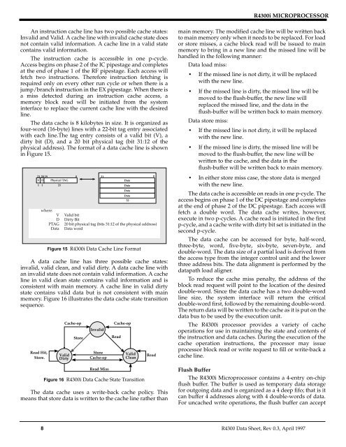
The data cache is 8 kilobytes in size. It is organized as<br />
four-word (16-byte) lines with a 22-bit tag entry associated<br />
with each line.The tag entry consists of a valid bit (V), a<br />
dirty bit (D), and a 20 bit physical tag (bit 31:12 of the<br />
physical address). The format of a data cache line is shown<br />
in Figure 15.<br />
21 20 19<br />
V D Physical TAG<br />
1 1<br />
21<br />
0<br />
Figure 15 <strong>R4300i</strong> Data Cache Line Format<br />
A data cache line has three possible cache states:<br />
invalid, valid clean, and valid dirty. A data cache line with<br />
an invalid state does not contain valid information. A cache<br />
line in valid clean state contains valid information and is<br />
consistent with main memory. A cache line in valid dirty<br />
state contains valid data but is not consistent with main<br />
memory. Figure 16 illustrates the data cache state transition<br />
sequence.<br />
Read Hit,<br />
Store.<br />
where:<br />
V<br />
D<br />
PTAG<br />
Data<br />
Figure 16 <strong>R4300i</strong> Data Cache State Transition<br />
The data cache uses a write-back cache policy. This<br />
means that store data is written to the cache line rather than<br />
31<br />
Data<br />
Data<br />
Data<br />
Data<br />
Valid bit<br />
Dirty Bit<br />
20 bit physical tag (bits 31:12 of the physical address)<br />
Data word<br />
Valid<br />
Dirty<br />
Cache-op<br />
Store<br />
Invalid<br />
Store<br />
Cache-op<br />
Read Miss<br />
Read<br />
32<br />
Cache-op<br />
Valid<br />
Clean<br />
0<br />
Read<br />
main memory. The modified cache line will be written back<br />
to main memory only when it needs to be replaced. For load<br />
or store misses, a cache block read will be issued to main<br />
memory to bring in a new line and the missed line will be<br />
handled in the following manner:<br />
Data load miss:<br />
• If the missed line is not dirty, it will be replaced<br />
with the new line.<br />
• If the missed line is dirty, the missed line will be<br />
moved to the flush-buffer, the new line will<br />
replaced the missed line, and the data in the<br />
flush-buffer will be written back to main memory.<br />
Data store miss:<br />
• If the missed line is not dirty, it will be replaced<br />
with the new line.<br />
• If the missed line is dirty, the missed line will be<br />
moved to the flush-buffer, the new line will be<br />
written to the cache, and the data in the<br />
flush-buffer will be written back to main memory.<br />
• In either store miss case, the store data is merged<br />
with the new line.<br />
The data cache is accessible on reads in one p-cycle. The<br />
access begins on phase 1 of the DC pipestage and completes<br />
at the end of phase 2 of the DC pipestage. Each access will<br />
fetch a double word. The data cache writes, however,<br />
execute in two p-cycles. A cache read is initiated in the first<br />
p-cycle, and a cache write with dirty bit set is initiated in the<br />
second p-cycle.<br />
The data cache can be accessed for byte, half-word,<br />
three-byte, word, five-byte, six-byte, seven-byte, and<br />
double-word. The data size of a partial load is derived from<br />
the access type from the integer control unit and the lower<br />
three address bits. The data alignment is performed by the<br />
datapath load aligner.<br />
To reduce the cache miss penalty, the address of the<br />
block read request will point to the location of the desired<br />
double-word. Since the data cache has a two double-word<br />
line size, the system interface will return the critical<br />
double-word first, followed by the remaining double-word.<br />
The return data will be written to the cache as it is put on the<br />
data bus to be used by the execution unit.<br />
The <strong>R4300i</strong> processor provides a variety of cache<br />
operations for use in maintaining the state and contents of<br />
the instruction and data caches. During the execution of the<br />
cache operation instructions, the processor may issue<br />
processor block read or write request to fill or write-back a<br />
cache line.<br />
Flush Buffer<br />
The <strong>R4300i</strong> Microprocessor contains a 4-entry on-chip<br />
flush buffer. The buffer is used as temporary data storage<br />
for outgoing data and is organized as a 4 deep fifo; that is it<br />
can buffer 4 addresses along with 4 double-words of data.<br />
For uncached write operations, the flush buffer can accept<br />
8 R4300 Data Sheet, Rev 0.3, April 1997