R4300i Product Information - MIPS Technologies, Inc.
R4300i Product Information - MIPS Technologies, Inc.
R4300i Product Information - MIPS Technologies, Inc.

You also want an ePaper? Increase the reach of your titles
YUMPU automatically turns print PDFs into web optimized ePapers that Google loves.
<strong>R4300i</strong> MICROPROCESSOR<br />
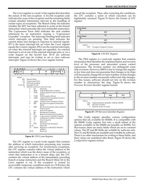
The Cause register is a read/write register that describes<br />
the nature of the last exception. A five-bit exception code<br />
indicates the cause of the exception and the remaining fields<br />
contain detailed information relevant to the handling of<br />
certain types of exceptions. The Branch Delay bit indicates<br />
whether the EPC has been adjusted to point at the branch<br />
instruction which precedes the next restartable instruction.<br />
The Coprocessor Error field indicates the unit number<br />
referenced by an instruction causing a “Coprocessor<br />
Unusable” exception. The Interrupt Pending field indicates<br />
which interrupts are pending. This field indicates the<br />
current status and changes in response to external signals.<br />
IP7 is the timer interrupt bit, set when the Count register<br />
equals the Compare register. IP6:2 are the external interrupts,<br />
set when the external interrupts are signalled. An external<br />
interrupt is set at one of the external interrupt pins or via a<br />
write request on the SysAD bus. IP1:0 are software<br />
interrupts, and may be written to set or clear software<br />
interrupts. Figure 32 shows the Cause register format.<br />
31 30 29 28 27<br />
16 15<br />
8 7 6 2 1 0<br />
BD 0 CE<br />
0<br />
IP 0 ExcCode 0<br />
1 1 2 12<br />
8 1 5 2<br />
where:<br />
BD Branch Delay<br />
CE Coprocessor Error<br />
IP Interrupt pending<br />
ExcCode Exception Code:<br />
0 Must be zeroes on read and write<br />
0 Int Interrupt<br />
1 Mod TLB modification exception<br />
2 TLBL TLB Exception (Load or instruction<br />
fetch)<br />
3 TLBS TLB Exception (Store)<br />
4 AdEL Address Error Exception (Load or<br />
instruction fetch)<br />
5 AdES Address Error Exception (Store)<br />
6 IBE Bus Error Exception (instruction<br />
fetch)<br />
7 DBE Bus Error Exception (data reference:<br />
load or store)<br />
8 Sys SysCall Exception<br />
9 Bp Breakpoint Exception<br />
10 RI Reserved instruction Exception<br />
11 CpU Coprocessor Unusable Exception<br />
12 Ov Arithmetic Overflow Exception<br />
13 Tr Trap Exception<br />
14 --- Reserved<br />
15 FPE Floating Point Exception<br />
16-22 Reserved<br />
23 Watch Reference to WatchHi/WatchLo<br />
address<br />
24-31 Reserved<br />
Figure 32 CP0 Cause Register<br />
The EPC register is a read/write register that contains<br />
the address at which instruction processing may resume<br />
after servicing an exception. For synchronous exceptions,<br />
the EPC register contains either the virtual address of the<br />
instruction which was the direct cause of the exception, or<br />
when that instruction is in a branch delay slot, the EPC<br />
contains the virtual address of the immediately preceding<br />
branch or jump instruction and the Branch Delay bit in the<br />
Cause register is set. If the exception is caused by<br />
recoverable, temporary conditions (such as a TLB miss), the<br />
EPC contains the virtual address of the instruction which<br />
caused the exception. Thus, after correcting the conditions,<br />
the EPC contains a point at which execution can be<br />
legitimately resumed. Figure 33 shows the format of EPC<br />
register.<br />
32 bit Mode:<br />
31 0<br />
EPC<br />
32<br />
64 bit Mode:<br />
63 0<br />
EPC<br />
64<br />
where:<br />
EPC Exception Program Counter.<br />
Figure 33 CP0 EPC Register<br />
The PRId register is a read-only register that contains<br />
information that identifies the implementation and revision<br />
level of the processor and associated system control<br />
coprocessor. The revision number can distinguish some<br />
chip revisions. However, <strong>MIPS</strong> is free to change this register<br />
at any time and does not guarantee that changes to its chips<br />
will necessarily change the revision number, or that changes<br />
to the revision number necessarily reflect real chip changes.<br />
For this reason, software should not rely on the revision<br />
number to characterize the chip. Figure 34 shows the<br />
Processor Revision Identifier register format.<br />
31 16 15<br />
8 7<br />
0<br />
0 Imp Rev<br />
16<br />
where:<br />
Imp Implementation identifier: 0x0B for <strong>R4300i</strong><br />
Rev Revision Number<br />
0 Returns zeroes on reads.<br />
Figure 34 CP0 Revision Identifier Register<br />
The Config register specifies various configuration<br />
options that are available for <strong>R4300i</strong>. It is compatible with<br />
the R4000 Config register, but only a small subset of the<br />
options available on the R4000 are possible on <strong>R4300i</strong>. For<br />
that reason, there are many fields which are set to constant<br />
values. The EP and BE fields are writable by software only.<br />
The CU and K0 fields are readable and writable by software.<br />
There is no other mechanism for writing to these fields, and<br />
their values are undefined after Reset. Figure 35 shows the<br />
Configuration register format.<br />
8<br />
8<br />
13 R4300 Data Sheet, Rev 0.3, April 1997