R4300i Product Information - MIPS Technologies, Inc.
R4300i Product Information - MIPS Technologies, Inc.
R4300i Product Information - MIPS Technologies, Inc.

Create successful ePaper yourself
Turn your PDF publications into a flip-book with our unique Google optimized e-Paper software.
<strong>R4300i</strong> MICROPROCESSOR<br />
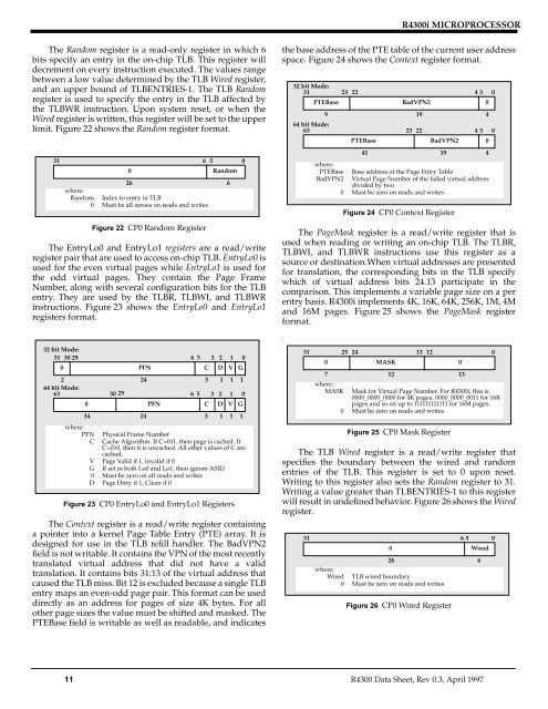
The Random register is a read-only register in which 6<br />
bits specify an entry in the on-chip TLB. This register will<br />
decrement on every instruction executed. The values range<br />
between a low value determined by the TLB Wired register,<br />
and an upper bound of TLBENTRIES-1. The TLB Random<br />
register is used to specify the entry in the TLB affected by<br />
the TLBWR instruction. Upon system reset, or when the<br />
Wired register is written, this register will be set to the upper<br />
limit. Figure 22 shows the Random register format.<br />
31 6 5 0<br />
0<br />
Random<br />
26<br />
6<br />
where:<br />
Random Index to entry in TLB<br />
0 Must be all zeroes on reads and writes<br />
Figure 22 CP0 Random Register<br />
The EntryLo0 and EntryLo1 registers are a read/write<br />
register pair that are used to access on-chip TLB. EntryLo0 is<br />
used for the even virtual pages while EntryLo1 is used for<br />
the odd virtual pages. They contain the Page Frame<br />
Number, along with several configuration bits for the TLB<br />
entry. They are used by the TLBR, TLBWI, and TLBWR<br />
instructions. Figure 23 shows the EntryLo0 and EntryLo1<br />
registers format.<br />
the base address of the PTE table of the current user address<br />
space. Figure 24 shows the Context register format.<br />
32 bit Mode:<br />
31 23 22<br />
4 3 0<br />
PTEBase<br />
BadVPN2<br />
0<br />
9<br />
19<br />
4<br />
64 bit Mode:<br />
63 23 22<br />
4 3 0<br />
PTEBase<br />
BadVPN2 0<br />
41<br />
19<br />
4<br />
where:<br />
PTEBase Base address of the Page Entry Table<br />
BadVPN2 Virtual Page Number of the failed virtual address<br />
divided by two<br />
0 Must be zero on reads and writes<br />
Figure 24 CP0 Context Register<br />
The PageMask register is a read/write register that is<br />
used when reading or writing an on-chip TLB. The TLBR,<br />
TLBWI, and TLBWR instructions use this register as a<br />
source or destination.When virtual addresses are presented<br />
for translation, the corresponding bits in the TLB specify<br />
which of virtual address bits 24.13 participate in the<br />
comparison. This implements a variable page size on a per<br />
entry basis. <strong>R4300i</strong> implements 4K, 16K, 64K, 256K, 1M, 4M<br />
and 16M pages. Figure 25 shows the PageMask register<br />
format.<br />
.<br />
32 bit Mode:<br />
31 30 29<br />
6 5 3 2 1 0<br />
0<br />
PFN<br />
C D V G<br />
2<br />
64 bit Mode:<br />
24<br />
3 1 1 1<br />
63 30 29<br />
6 5 3 2 1 0<br />
0<br />
PFN<br />
C D V G<br />
34<br />
24<br />
3 1 1 1<br />
where:<br />
PFN Physical Frame Number<br />
C Cache Algorithm. If C=011, then page is cached. If<br />
C=010, then it is uncached. All other values of C are<br />
cached.<br />
V Page Valid if 1, invalid if 0<br />
G If set in both Lo0 and Lo1, then ignore ASID<br />
0 Must be zero on all reads and writes<br />
D Page Dirty if 1, Clean if 0<br />
Figure 23 CP0 EntryLo0 and EntryLo1 Registers<br />
The Context register is a read/write register containing<br />
a pointer into a kernel Page Table Entry (PTE) array. It is<br />
designed for use in the TLB refill handler. The BadVPN2<br />
field is not writable. It contains the VPN of the most recently<br />
translated virtual address that did not have a valid<br />
translation. It contains bits 31:13 of the virtual address that<br />
caused the TLB miss. Bit 12 is excluded because a single TLB<br />
entry maps an even-odd page pair. This format can be used<br />
directly as an address for pages of size 4K bytes. For all<br />
other page sizes the value must be shifted and masked. The<br />
PTEBase field is writable as well as readable, and indicates<br />
31 25 24<br />
13 12<br />
0<br />
0<br />
MASK<br />
0<br />
7<br />
12<br />
13<br />
where:<br />
MASK Mask for Virtual Page Number. For <strong>R4300i</strong>, this is<br />
0000_0000_0000 for 4K pages, 0000_0000_0011 for 16K<br />
pages and so on up to 111111111111 for 16M pages.<br />
0 Must be zero on reads and writes<br />
Figure 25 CP0 Mask Register<br />
The TLB Wired register is a read/write register that<br />
specifies the boundary between the wired and random<br />
entries of the TLB. This register is set to 0 upon reset.<br />
Writing to this register also sets the Random register to 31.<br />
Writing a value greater than TLBENTRIES-1 to this register<br />
will result in undefined behavior. Figure 26 shows the Wired<br />
register.<br />
31 6 5 0<br />
0<br />
26<br />
Wired<br />
6<br />
where:<br />
Wired TLB wired boundary<br />
0 Must be zero on reads and writes<br />
Figure 26 CP0 Wired Register<br />
11 R4300 Data Sheet, Rev 0.3, April 1997