R4300i Product Information - MIPS Technologies, Inc.
R4300i Product Information - MIPS Technologies, Inc.
R4300i Product Information - MIPS Technologies, Inc.

You also want an ePaper? Increase the reach of your titles
YUMPU automatically turns print PDFs into web optimized ePapers that Google loves.
<strong>R4300i</strong> MICROPROCESSOR<br />
31 30 28 27 24 23 20 19 18 1716 15 14 13 12 11 9 8 6 5 4 3 2 0<br />
0 EC EP 0000 01 1 0<br />
B<br />
1 1 0 010 001 1 0 C K0<br />
E<br />
U<br />
4 4 4 2 1 1 1 1 1 1 3 3 1 1 1 3<br />
where:<br />
EC<br />
EP<br />
BE<br />
CU<br />
K0<br />
System Clock Ratio: Read only<br />
110 = 1:1<br />
111 = 1.5:1<br />
000 = 2:1<br />
001 = 3:1<br />
All other values of EC are undefined.<br />
Pattern for writeback data on SYSAD port<br />
0000 -> D<br />
0110 -> DxxDxx<br />
All other values of EP are undefined.<br />
BigEndianMem<br />
0 -> Memory and kernel are Little Endian<br />
1 -> Memory and kernel are Big Endian<br />
Reserved. (Read- and Writ-able by software)<br />
Kseg0 coherency algorithm. This has the same format<br />
as the C field in EntryLo0 and EntryLo1. The only<br />
defined values for K0 for <strong>R4300i</strong> are 010<br />
(noncacheable) and 011 (cacheable).<br />
0 Returns 0 on read.<br />
1 Returns 1 on read.<br />
Figure 35 CP0 Configuration Register<br />
The <strong>R4300i</strong>i processor provides a debugging feature to<br />
detect references to a physical address. Loads or stores to<br />
the location specified by the WatchHi/WatchLo register pair<br />
cause a Watch trap. Figure 36 shows WatchHi/WatchLo<br />
register formats.<br />
WatchLo:<br />
31 3 2 1 0<br />
PAddr<br />
0 R W<br />
29<br />
1 1 1<br />
WatchHi:<br />
31 4 3 0<br />
0<br />
PAddr<br />
31<br />
4<br />
where:<br />
PAddr Physical address<br />
WatchLo PAddr contains bits 31.3<br />
In the <strong>R4300i</strong> bits 3:0 of the WatchHi register<br />
are ignored but are software writable. This<br />
is to maintain compatibility with the R4000.<br />
R Trap on Read Access if 1<br />
W Trap on Write Access if 1<br />
0 Must be zeroes on reads and writes<br />
Figure 36 CP0 WatchLo and WatchHi Registers<br />
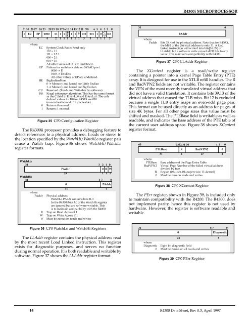
The LLAddr register contains the physical address read<br />
by the most recent Load Linked instruction. This register<br />
exists for diagnostic purposes, and serves no function<br />
during normal operation. It is both readable and writable by<br />
software. Figure 37 shows the LLAddr register format.<br />
31 0<br />
where:<br />
Paddr<br />
PAddr<br />
Bits 35..4 of the physical address. Note that for <strong>R4300i</strong>,<br />
the MSB of the physical address is only 31. A load<br />
linked instruction will write 0 into bits[31..29] of<br />
LLAddr, but a software write can set all 32 bits to any<br />
value. This maintains compatibility with R4000.<br />
Figure 37 CP0 LLAddr Register<br />
The XContext register is a read/write register<br />
containing a pointer into a kernel Page Table Entry (PTE)<br />
array. It is designed for use in the XTLB refill handler. The R<br />
and BadVPN2 fields are not writable. The register contains<br />
the VPN of the most recently translated virtual address that<br />
did not have a valid translation. It contains bits 39.13 of the<br />
virtual address that caused the TLB miss. Bit 12 is excluded<br />
because a single TLB entry maps an even-odd page pair.<br />
This format can be used directly as an address for pages of<br />
size 4K bytes. For all other page sizes this value must be<br />
shifted and masked. The PTEBase field is writable as well as<br />
readable, and indicates the base address of the PTE table of<br />
the current user address space. Figure 38 shows XContext<br />
register format.<br />
63 3332 31 30<br />
4 3 0<br />
PTEBase R BadVPN2 0<br />
31<br />
2<br />
27<br />
4<br />
where:<br />
PTEBase Base address of the Page Entry Table<br />
BadVPN2 Virtual Page Number of the failed virtual address<br />
divided by two<br />
R Region (00=user, 01=supervisor, 11=kernel)<br />
0 Must be zero on reads and writes<br />
Figure 38 CP0 XContext Register<br />
The PErr register, shown in Figure 39, is included only<br />
to maintain compatibility with the R4200. The <strong>R4300i</strong> does<br />
not implement parity, hence this register is not used by<br />
hardware. However, the register is software readable and<br />
writable.<br />
31 8 7 0<br />
0<br />
24<br />
Diagnostic<br />
8<br />
where:<br />
Diagnostic Eight bit diagnostic field<br />
0 Must be zeroes on all reads and writes<br />
Figure 39 CP0 PErr Register<br />
14 R4300 Data Sheet, Rev 0.3, April 1997