R4300i Product Information - MIPS Technologies, Inc.
R4300i Product Information - MIPS Technologies, Inc.
R4300i Product Information - MIPS Technologies, Inc.

You also want an ePaper? Increase the reach of your titles
YUMPU automatically turns print PDFs into web optimized ePapers that Google loves.
<strong>R4300i</strong> MICROPROCESSOR<br />
PClock<br />
Phase<br />
Cycle<br />
Instr. Fetch<br />
Instr. Decode<br />
Reg. File Read<br />
Arithmetic/Logical<br />
Operations<br />
Load/Store<br />
Operations<br />
Jump/Branch<br />
Operations<br />
Φ1 Φ2 Φ1 Φ2 Φ1 Φ2 Φ1 Φ2 Φ1 Φ2<br />
IC RF EX DC WB<br />
ITLB<br />
ICF<br />
ITC<br />
IDEC<br />
RFR<br />
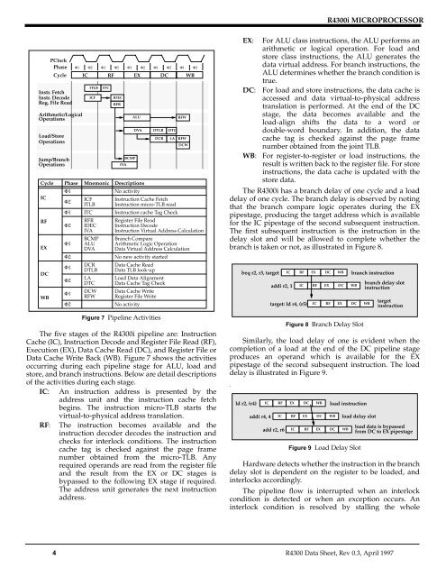
Figure 7 Pipeline Activities<br />
The five stages of the <strong>R4300i</strong> pipeline are: Instruction<br />
Cache (IC), Instruction Decode and Register File Read (RF),<br />
Execution (EX), Data Cache Read (DC), and Register File or<br />
Data Cache Write Back (WB). Figure 7 shows the activities<br />
occurring during each pipeline stage for ALU, load and<br />
store, and branch instructions. Below are detail descriptions<br />
of the activities during each stage.<br />
IC: An instruction address is presented by the<br />
address unit and the instruction cache fetch<br />
begins. The instruction micro-TLB starts the<br />
virtual-to-physical address translation.<br />
RF: The instruction becomes available and the<br />
instruction decoder decodes the instruction and<br />
checks for interlock conditions. The instruction<br />
cache tag is checked against the page frame<br />
number obtained from the micro-TLB. Any<br />
required operands are read from the register file<br />
and the result from the EX or DC stages is<br />
bypassed to the following EX stage if required.<br />
The address unit generates the next instruction<br />
address.<br />
ALU<br />
BCMP<br />
IVA<br />
DVA<br />
Cycle Phase Mnemonic Descriptions<br />
IC<br />
RF<br />
EX<br />
DC<br />
WB<br />
Φ1<br />
Φ2<br />
ICF<br />
ITLB<br />
No activity<br />
RFW<br />
DTLB DTC<br />
DCR LA RFW<br />
Instruction Cache Fetch<br />
Instruction micro-TLB read<br />
Φ1 ITC Instruction cache Tag Check<br />
Φ2<br />
Φ1<br />
Φ2<br />
Φ1<br />
Φ2<br />
Φ1<br />
Φ2<br />
RFR<br />
IDEC<br />
IVA<br />
BCMP<br />
ALU<br />
DVA<br />
DCR<br />
DTLB<br />
LA<br />
DTC<br />
DCW<br />
RFW<br />
DCW<br />
Register File Read<br />
Instruction Decode<br />
Instruction Virtual Address Calculation<br />
Branch Compare<br />
Arithmetic Logic Operation<br />
Data Virtual Address Calculation<br />
No new activity started<br />
Data Cache Read<br />
Data TLB look-up<br />
Load Data Alignment<br />
Data Cache Tag Check<br />
Data Cache Write<br />
Register File Write<br />
No activity<br />
EX: For ALU class instructions, the ALU performs an<br />
arithmetic or logical operation. For load and<br />
store class instructions, the ALU generates the<br />
data virtual address. For branch instructions, the<br />
ALU determines whether the branch condition is<br />
true.<br />
DC: For load and store instructions, the data cache is<br />
accessed and data virtual-to-physical address<br />
translation is performed. At the end of the DC<br />
stage, the data becomes available and the<br />
load-align shifts the data to a word or<br />
double-word boundary. In addition, the data<br />
cache tag is checked against the page frame<br />
number obtained from the joint TLB.<br />
WB: For register-to-register or load instructions, the<br />
result is written back to the register file. For store<br />
instructions, the data cache is updated with the<br />
store data.<br />
The <strong>R4300i</strong> has a branch delay of one cycle and a load<br />
delay of one cycle. The branch delay is observed by noting<br />
that the branch compare logic operates during the EX<br />
pipestage, producing the target address which is available<br />
for the IC pipestage of the second subsequent instruction.<br />
The first subsequent instruction is the instruction in the<br />
delay slot and will be allowed to complete whether the<br />
branch is taken or not, as illustrated in Figure 8.<br />
Figure 8 Branch Delay Slot<br />
Similarly, the load delay of one is evident when the<br />
completion of a load at the end of the DC pipeline stage<br />
produces an operand which is available for the EX<br />
pipestage of the second subsequent instruction. The load<br />
delay is illustrated in Figure 9.<br />
.<br />
beq r2, r3, target<br />
ld r2, (r4)<br />
addi r4, 4<br />
addi r2, 1<br />
IC RF EX DC WB<br />
target: ld r4, (r5)<br />
IC RF EX DC WB<br />
add r2, r6<br />
IC RF EX DC WB<br />
IC RF EX DC WB<br />
IC RF EX DC WB<br />
load instruction<br />
IC RF EX DC WB<br />
Figure 9 Load Delay Slot<br />
branch instruction<br />
load delay slot<br />
branch delay slot<br />
instruction<br />
target<br />
instruction<br />
load data is bypassed<br />
from DC to EX pipestage<br />
Hardware detects whether the instruction in the branch<br />
delay slot is dependent on the register to be loaded, and<br />
interlocks accordingly.<br />
The pipeline flow is interrupted when an interlock<br />
condition is detected or when an exception occurs. An<br />
interlock condition is resolved by stalling the whole<br />
4 R4300 Data Sheet, Rev 0.3, April 1997