R4300i Product Information - MIPS Technologies, Inc.
R4300i Product Information - MIPS Technologies, Inc.
R4300i Product Information - MIPS Technologies, Inc.

Create successful ePaper yourself
Turn your PDF publications into a flip-book with our unique Google optimized e-Paper software.
<strong>R4300i</strong> MICROPROCESSOR<br />
cycles between any two data cycles. However, for this<br />
implementation (i.e. <strong>R4300i</strong>) the data will begin on the cycle<br />
immediately following the write issue cycle, and transfers<br />
data at a programmed cycle data rate thereafter. The<br />
processor drives data at the rate specified by the data rate<br />
configuration signals.<br />
Writes may be cancelled and retried with the EOK<br />
signal.<br />
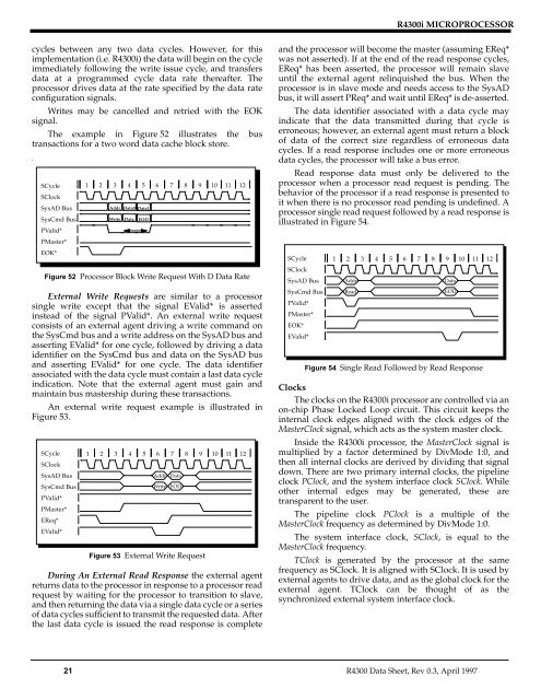
The example in Figure 52 illustrates the bus<br />
transactions for a two word data cache block store.<br />
.<br />
SCycle 1 2 3 4 5 6 7 8 9 10 11 12<br />
SClock<br />
SysAD Bus<br />
Addr Data0 Data1<br />
SysCmd Bus Write Data EOD<br />
PValid*<br />
PMaster*<br />
EOK*<br />
Figure 52 Processor Block Write Request With D Data Rate<br />
External Write Requests are similar to a processor<br />
single write except that the signal EValid* is asserted<br />
instead of the signal PValid*. An external write request<br />
consists of an external agent driving a write command on<br />
the SysCmd bus and a write address on the SysAD bus and<br />
asserting EValid* for one cycle, followed by driving a data<br />
identifier on the SysCmd bus and data on the SysAD bus<br />
and asserting EValid* for one cycle. The data identifier<br />
associated with the data cycle must contain a last data cycle<br />
indication. Note that the external agent must gain and<br />
maintain bus mastership during these transactions.<br />
An external write request example is illustrated in<br />
Figure 53.<br />
SCycle 1 2 3 4 5 6 7 8 9 10 11 12<br />
SClock<br />
SysAD Bus<br />
SysCmd Bus<br />
PValid*<br />
PMaster*<br />
EReq*<br />
EValid*<br />
Addr<br />
Figure 53 External Write Request<br />
During An External Read Response the external agent<br />
returns data to the processor in response to a processor read<br />
request by waiting for the processor to transition to slave,<br />
and then returning the data via a single data cycle or a series<br />
of data cycles sufficient to transmit the requested data. After<br />
the last data cycle is issued the read response is complete<br />
Data<br />
Write EOD<br />
and the processor will become the master (assuming EReq*<br />
was not asserted). If at the end of the read response cycles,<br />
EReq* has been asserted, the processor will remain slave<br />
until the external agent relinquished the bus. When the<br />
processor is in slave mode and needs access to the SysAD<br />
bus, it will assert PReq* and wait until EReq* is de-asserted.<br />
The data identifier associated with a data cycle may<br />
indicate that the data transmitted during that cycle is<br />
erroneous; however, an external agent must return a block<br />
of data of the correct size regardless of erroneous data<br />
cycles. If a read response includes one or more erroneous<br />
data cycles, the processor will take a bus error.<br />
Read response data must only be delivered to the<br />
processor when a processor read request is pending. The<br />
behavior of the processor if a read response is presented to<br />
it when there is no processor read pending is undefined. A<br />
processor single read request followed by a read response is<br />
illustrated in Figure 54.<br />
SCycle 1 2 3 4 5 6 7 8 9 10 11 12<br />
SClock<br />
SysAD Bus<br />
SysCmd Bus<br />
PValid*<br />
PMaster*<br />
EOK*<br />
EValid*<br />
Addr<br />
Read<br />
Data<br />
EOD<br />
Figure 54 Single Read Followed by Read Response<br />
Clocks<br />
The clocks on the <strong>R4300i</strong> processor are controlled via an<br />
on-chip Phase Locked Loop circuit. This circuit keeps the<br />
internal clock edges aligned with the clock edges of the<br />
MasterClock signal, which acts as the system master clock.<br />
Inside the <strong>R4300i</strong> processor, the MasterClock signal is<br />
multiplied by a factor determined by DivMode 1:0, and<br />
then all internal clocks are derived by dividing that signal<br />
down. There are two primary internal clocks, the pipeline<br />
clock PClock, and the system interface clock SClock. While<br />
other internal edges may be generated, these are<br />
transparent to the user.<br />
The pipeline clock PClock is a multiple of the<br />
MasterClock frequency as determined by DivMode 1:0.<br />
The system interface clock, SClock, is equal to the<br />
MasterClock frequency.<br />
TClock is generated by the processor at the same<br />
frequency as SClock. It is aligned with SClock. It is used by<br />
external agents to drive data, and as the global clock for the<br />
external agent. TClock can be thought of as the<br />
synchronized external system interface clock.<br />
21 R4300 Data Sheet, Rev 0.3, April 1997