R4300i Product Information - MIPS Technologies, Inc.
R4300i Product Information - MIPS Technologies, Inc.
R4300i Product Information - MIPS Technologies, Inc.

You also want an ePaper? Increase the reach of your titles
YUMPU automatically turns print PDFs into web optimized ePapers that Google loves.
<strong>R4300i</strong> MICROPROCESSOR<br />
These all combine to produce the low average power<br />
dissipation that allows the <strong>R4300i</strong> to be a practical<br />
battery-powered processor.<br />
Differences Between The <strong>R4300i</strong> And R4200<br />
The primary differences between <strong>R4300i</strong> and the R4200<br />
are the system interface bus architecture and the absence of<br />
parity. The low-cost package requirements of the <strong>R4300i</strong><br />
necessitated a new bus definition, which is very similar to<br />
but not the same as the R4200 system interface bus.<br />
The functional differences between the R4200 and the<br />
<strong>R4300i</strong> processor’s that are visible to software are contained<br />
in the Coprocessor 0 implementation.<br />
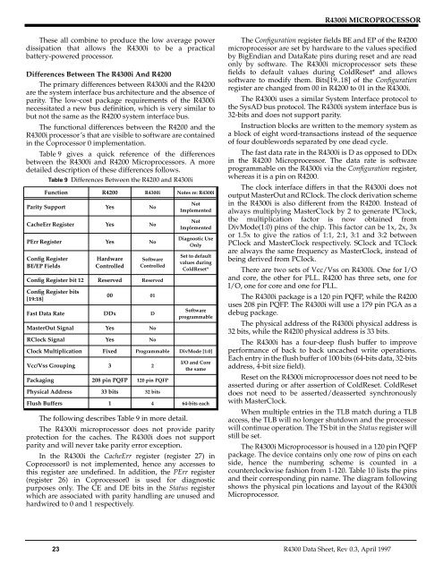
Table 9 gives a quick reference of the differences<br />
between the <strong>R4300i</strong> and R4200 Microprocessors. A more<br />
detailed description of these differences follows.<br />
Table 9 Differences Between the R4200 and <strong>R4300i</strong><br />
Function R4200 <strong>R4300i</strong> Notes re: <strong>R4300i</strong><br />
Parity Support Yes No<br />
CacheErr Register Yes No<br />
PErr Register Yes No<br />
Config Register<br />
BE/EP Fields<br />
Hardware<br />
Controlled<br />
Software<br />
Controlled<br />
Config Register bit 12 Reserved Reserved<br />
Config Register bits<br />
[19:18]<br />
00 01<br />
Fast Data Rate DDx D<br />
MasterOut Signal Yes No<br />
RClock Signal Yes No<br />
Not<br />
Implemented<br />
Not<br />
Implemented<br />
Diagnostic Use<br />
Only<br />
Set to default<br />
values during<br />
ColdReset*<br />
Software<br />
programmable<br />
Clock Multiplication Fixed Programmable DivMode [1:0]<br />
Vcc/Vss Grouping 3 2<br />
Packaging 208 pin PQFP 120 pin PQFP<br />
Physical Address 33 bits 32 bits<br />
I/O and Core<br />
the same<br />
Flush Buffers 1 4 64-bits each<br />
The following describes Table 9 in more detail.<br />
The <strong>R4300i</strong> microprocessor does not provide parity<br />
protection for the caches. The <strong>R4300i</strong> does not support<br />
parity and will never take parity error exception.<br />
In the <strong>R4300i</strong> the CacheErr register (register 27) in<br />
Coprocessor0 is not implemented, hence any accesses to<br />
this register are undefined. In addition, the PErr register<br />
(register 26) in Coprocessor0 is used for diagnostic<br />
purposes only. The CE and DE bits in the Status register<br />
which are associated with parity handling are unused and<br />
hardwired to 0 and 1 respectively.<br />
The Configuration register fields BE and EP of the R4200<br />
microprocessor are set by hardware to the values specified<br />
by BigEndian and DataRate pins during reset and are read<br />
only by software. The <strong>R4300i</strong> microprocessor sets these<br />
fields to default values during ColdReset* and allows<br />
software to modify them. Bits[19..18] of the Configuration<br />
register are changed from 00 in R4200 to 01 in the <strong>R4300i</strong>.<br />
The <strong>R4300i</strong> uses a similar System Interface protocol to<br />
the SysAD bus protocol. The <strong>R4300i</strong> system interface bus is<br />
32-bits and does not support parity.<br />
Instruction blocks are written to the memory system as<br />
a block of eight word-transactions instead of the sequence<br />
of four doublewords separated by one dead cycle.<br />
The fast data rate in the <strong>R4300i</strong> is D as opposed to DDx<br />
in the R4200 Microprocessor. The data rate is software<br />
programmable on the <strong>R4300i</strong> via the Configuration register,<br />
whereas it is a pin on R4200.<br />
The clock interface differs in that the <strong>R4300i</strong> does not<br />
output MasterOut and RClock. The clock derivation scheme<br />
in the <strong>R4300i</strong> is also different from the R4200. Instead of<br />
always multiplying MasterClock by 2 to generate PClock,<br />
the multiplication factor is now obtained from<br />
DivMode(1:0) pins of the chip. This factor can be 1x, 2x, 3x<br />
or 1.5x to give the ratios of 1:1, 2:1, 3:1 and 3:2 between<br />
PClock and MasterClock respectively. SClock and TClock<br />
are always the same frequency as MasterClock, instead of<br />
being derived from PClock.<br />
There are two sets of Vcc/Vss on <strong>R4300i</strong>. One for I/O<br />
and core, the other for PLL. R4200 has three sets, one for<br />
I/O, one for core and one for PLL.<br />
The <strong>R4300i</strong> package is a 120 pin PQFP, while the R4200<br />
uses 208 pin PQFP. The <strong>R4300i</strong> will use a 179 pin PGA as a<br />
debug package.<br />
The physical address of the <strong>R4300i</strong> physical address is<br />
32 bits, while the R4200 physical address is 33 bits.<br />
The <strong>R4300i</strong> has a four-deep flush buffer to improve<br />
performance of back to back uncached write operations.<br />
Each entry in the flush buffer of 100 bits (64-bits data, 32-bits<br />
address, 4-bit size field).<br />
Reset on the <strong>R4300i</strong> microprocessor does not need to be<br />
asserted during or after assertion of ColdReset. ColdReset<br />
does not need to be asserted/deasserted synchronously<br />
with MasterClock.<br />
When multiple entries in the TLB match during a TLB<br />
access, the TLB will no longer shutdown and the processor<br />
will continue operation. The TS bit in the Status register will<br />
still be set.<br />
The <strong>R4300i</strong> Microprocessor is housed in a 120 pin PQFP<br />
package. The device contains only one row of pins on each<br />
side, hence the numbering scheme is counted in a<br />
counterclockwise fashion from 1-120. Table 10 lists the pins<br />
and their corresponding pin name. The diagram following<br />
shows the physical pin locations and layout of the <strong>R4300i</strong><br />
Microprocessor.<br />
23 R4300 Data Sheet, Rev 0.3, April 1997