R4300i Product Information - MIPS Technologies, Inc.
R4300i Product Information - MIPS Technologies, Inc.
R4300i Product Information - MIPS Technologies, Inc.

You also want an ePaper? Increase the reach of your titles
YUMPU automatically turns print PDFs into web optimized ePapers that Google loves.
<strong>R4300i</strong> MICROPROCESSOR<br />
For load and store class instructions, the datapath can<br />
handle partial-words in either big- or little-endian mode.<br />
For store instructions, the main bi-directional shifter<br />
performs an alignment shift on the register read data. No<br />
concatenation of register read data with the original<br />
memory data is necessary since the data cache has byte<br />
write enable controls. For load instructions, it is necessary to<br />
maintain a load delay of one pclock cycle. Due to the timing<br />
requirements imposed by this load delay, a dedicated<br />
byte-wide shifter (Load Aligner) is needed to shift the<br />
memory read data in bytes, halfwords, and words in the<br />
right or left direction.<br />
The operand bypass network is built into the datapath<br />
to allow feedback of results from the EX and DC pipeline<br />
stages to the instructions in the following EX pipestage<br />
waiting to use the results as source operands rs and/or rt.<br />
This allows the following instruction to proceed without<br />
having to wait for the results to be written back to the<br />
register file. Similarly, to maintain the minimum branch<br />
delay slot of one pipeline clock cycle for all branch<br />
instructions on the floating-point condition, the results from<br />
the preceding floating-point compare instruction in the EX,<br />
DC, or WB pipestage will be fed back for branch condition<br />
testing in the RF pipestage.<br />
The exponent datapath is 12 bits wide. The twelfth bit<br />
(MSB) is used as both sign bit and overflow bit. The<br />
exponent datapath consists of a feedback mux and 2<br />
operand muxes to select the inputs from the adder, constant<br />
generating logic, a carry select adder, random logic to<br />
perform exception detection, and a register to hold the<br />
selected result from the adder, as shown in Figure 12.<br />
The inputs to the exponent unit come from the unpack<br />
logic, where the exponents are extracted from single- or<br />
double-precision floating-point operands. The<br />
carry-selected adder performs exponent subtraction,<br />
pre-alignment shift calculation, and exponent addition for<br />
post-normalization final update. The result is sent to the<br />
repack logic to be merged with the mantissa.<br />
The result of the exponent logic is compared with<br />
constants or ranges to check for various conditions by the<br />
result checker. These conditions include: underflow,<br />
overflow in single-precision number, overflow in<br />
double-precision number, one, zero, and convert limit<br />
check. The checks are performed as soon as data is available<br />
from the carry-select adder.<br />
The instruction virtual address unit is responsible for<br />
the generation of 64-bit instruction virtual addresses to be<br />
used by the micro-TLB, I-Cache and CP0. It has its own<br />
incrementor to calculate the next sequential address. It also<br />
has an equality comparator and a separate ripple-carry<br />
adder to generate the branch target address.<br />
In addition, the address unit has exception vector<br />
generator logic to decode the type of exception and then<br />
present the appropriate vector as the next PC address. It<br />
also has the exception PC register pipe chain to maintain a<br />
history of PC addresses for each pipestage so that the PC<br />
address associated with the exception causing instruction<br />
can be loaded into the Exception Program Counter (EPC)<br />
register.<br />
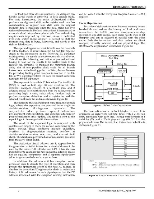
Cache Organization<br />
To achieve high performance, increase memory access<br />
bandwidth and reduce the latency of load and store<br />
instructions, the <strong>R4300i</strong> processor incorporates on-chip<br />
instruction and data caches. Each cache has its own 64-bit<br />
datapath and can be accessed in parallel with the other<br />
cache. Both the instruction and data caches are direct<br />
mapped, virtually indexed, and use physical tags. The<br />
<strong>R4300i</strong> cache organization is shown in Figure 13.<br />
D-Cache<br />
SysAD Output Data Path<br />
PAD Ring<br />
Flush-Buffer<br />
DBus<br />
32<br />
Data-Path/<br />
Control<br />
DTAG ITAG<br />
Cache<br />
Cntl<br />
SysAD Bus<br />
SysAD Input<br />
Data Path<br />
IBus<br />
Figure 13 <strong>R4300i</strong> Cache Organization<br />
The instruction cache is 16 kilobytes in size. It is<br />
organized as eight-word (32-byte) lines with a 21-bit tag<br />
entry associated with each line. The tag entry consists of a<br />
valid bit (V), and a 20-bit physical tag (bit 31:12 of the<br />
physical address). The format of an instruction cache line is<br />
shown in Figure 14.<br />
20 19<br />
V<br />
1<br />
Physical TAG<br />
20<br />
where:<br />
V<br />
PTAG<br />
Data<br />
Figure 14 <strong>R4300i</strong> Instruction Cache Line Form<br />
64<br />
64 64<br />
0<br />
31<br />
Data<br />
Data<br />
Data<br />
Data<br />
Data<br />
Data<br />
Data<br />
Data<br />
32<br />
I-Cache<br />
Valid bit<br />
20 bit physical tag (bit 31:12 of the physical address)<br />
Data word<br />
0<br />
7 R4300 Data Sheet, Rev 0.3, April 1997