R4300i Product Information - MIPS Technologies, Inc.
R4300i Product Information - MIPS Technologies, Inc.
R4300i Product Information - MIPS Technologies, Inc.

You also want an ePaper? Increase the reach of your titles
YUMPU automatically turns print PDFs into web optimized ePapers that Google loves.
<strong>R4300i</strong> MICROPROCESSOR<br />
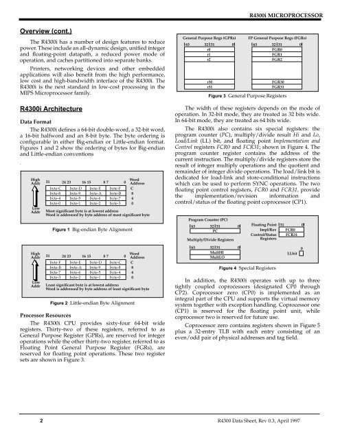
Overview (cont.)<br />
The <strong>R4300i</strong> has a number of design features to reduce<br />
power. These include an all-dynamic design, unified integer<br />
and floating-point datapath, a reduced power mode of<br />
operation, and caches partitioned into separate banks.<br />
Printers, networking devices and other embedded<br />
applications will also benefit from the high performance,<br />
low cost and high-bandwidth interface of the <strong>R4300i</strong>. The<br />
<strong>R4300i</strong> is the next standard in low-cost processing in the<br />
<strong>MIPS</strong> Microprocessor family.<br />
<strong>R4300i</strong> Architecture<br />
Data Format<br />
The <strong>R4300i</strong> defines a 64-bit double-word, a 32-bit word,<br />
a 16-bit halfword and an 8-bit byte. The byte ordering is<br />
configurable in either Big-endian or Little-endian format.<br />
Figures 1 and 2 show the ordering of bytes for Big-endian<br />
and Little-endian conventions<br />
.<br />
High<br />
Addr<br />
Low<br />
Addr<br />
High<br />
Addr<br />
Low<br />
Addr<br />
31 24 23 16 15 8 7 0<br />
byte-C byte-D byte-E byte-F<br />
byte-8 byte-9 byte-A byte-B<br />
byte-4 byte-5 byte-6 byte-7<br />
byte-0 byte-1 byte-2 byte-3<br />
Figure 1 Big-endian Byte Alignment<br />
Figure 2 Little-endian Byte Alignment<br />
Word<br />
Address<br />
C<br />
8<br />
4<br />
0<br />
Most significant byte is at lowest address<br />
Word is addressed by byte address of most significant byte<br />
31 24 23 16 15 8 7 0<br />
byte-F byte-E byte-D byte-C<br />
byte-B byte-A byte-9 byte-8<br />
byte-7 byte-6 byte-5 byte-4<br />
byte-3 byte-2 byte-1 byte-0<br />
Word<br />
Address<br />
C<br />
8<br />
4<br />
0<br />
Least significant byte is at lowest address<br />
Word is addressed by byte address of least significant byte<br />
Processor Resources<br />
The <strong>R4300i</strong> CPU provides sixty-four 64-bit wide<br />
registers. Thirty-two of these registers, referred to as<br />
General Purpose Register (GPRs), are reserved for integer<br />
operations while the other thirty-two register, referred to as<br />
Floating Point General Purpose Register (FGRs), are<br />
reserved for floating point operations. These two register<br />
sets are shown in Figure 3.<br />
General Purpose Regs (GPRs)<br />
63 32 31 0<br />
r0<br />
r1<br />
r2<br />
r30<br />
r31<br />
FP General Purpose Regs (FGRs)<br />
63 32 31 0<br />
FGR0<br />
FGR1<br />
FGR2<br />
Figure 3 General Purpose Registers<br />
The width of these registers depends on the mode of<br />
operation. In 32-bit mode, they are treated as 32 bits wide.<br />
In 64-bit mode, they are treated as 64 bits wide.<br />
The <strong>R4300i</strong> also contains six special registers: the<br />
program counter (PC), multiply/divide result Hi and Lo,<br />
Load/Link (LL) bit, and floating point Implementation and<br />
Control registers FCR0 and FCR31; shown in Figure 4. The<br />
program counter register contains the address of the<br />
current instruction. The multiply/divide registers store the<br />
result of integer multiply operations and the quotient and<br />
remainder of integer divide operations. The load/link bit is<br />
dedicated for load-link and store-conditional instructions<br />
which can be used to perform SYNC operations. The two<br />
floating point control registers, FCR0 and FCR31, provide<br />
the implementation/revision information and<br />
control/status of the floating point coprocessor (CP1).<br />
Program Counter (PC)<br />
63<br />
32 31<br />
PC<br />
Multiply/Divide Registers<br />
63<br />
32 31<br />
MultHI<br />
MultLO<br />
0<br />
0<br />
Floating Point<br />
Impl/Rev<br />
Control/Status<br />
Registers<br />
Figure 4 Special Registers<br />
FGR30<br />
FGR31<br />
In addition, the <strong>R4300i</strong> operates with up to three<br />
tightly coupled coprocessors (designated CP0 through<br />
CP2). Coprocessor zero (CP0) is implemented as an<br />
integral part of the CPU and supports the virtual memory<br />
system together with exception handling. Coprocessor one<br />
(CP1) is reserved for the floating point unit, while<br />
coprocessor two is reserved for future use.<br />
Coprocessor zero contains registers shown in Figure 5<br />
plus a 32-entry TLB with each entry consisting of an<br />
even/odd pair of physical addresses and tag field.<br />
31<br />
FCR0<br />
FCR31<br />
LLbit<br />
0<br />
0<br />
2 R4300 Data Sheet, Rev 0.3, April 1997