R4300i Product Information - MIPS Technologies, Inc.
R4300i Product Information - MIPS Technologies, Inc.
R4300i Product Information - MIPS Technologies, Inc.

You also want an ePaper? Increase the reach of your titles
YUMPU automatically turns print PDFs into web optimized ePapers that Google loves.
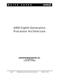
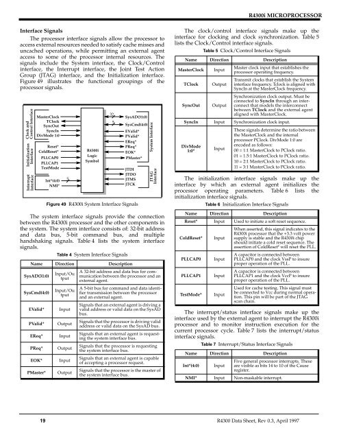
<strong>R4300i</strong> MICROPROCESSOR<br />
Interface Signals<br />
The processor interface signals allow the processor to<br />
access external resources needed to satisfy cache misses and<br />
uncached operations, while permitting an external agent<br />
access to some of the processor internal resources. The<br />
signals include the System interface, the Clock/Control<br />
interface, the Interrupt interface, the Joint Test Action<br />
Group (JTAG) interface, and the Initialization interface.<br />
Figure 49 illustrates the functional groupings of the<br />
processor signals.<br />
Clock and<br />
Control Interface<br />
Initialization<br />
Interface<br />
Interrupt<br />
Interface<br />
MasterClock<br />
TClock<br />
SyncOut<br />
SyncIn<br />
DivMode 1:0<br />
Figure 49 <strong>R4300i</strong> System Interface Signals<br />
The system interface signals provide the connection<br />
between the <strong>R4300i</strong> processor and the other components in<br />
the system. The system interface consists of: 32-bit address<br />
and data bus, 5-bit command bus, and multiple<br />
handshaking signals. Table 4 lists the system interface<br />
signals.<br />
Table 4 System Interface Signals<br />
Name Direction Description<br />
SysAD(31:0)<br />
SysCmd(4:0)<br />
EValid*<br />
PValid*<br />
EReq*<br />
PReq*<br />
EOK*<br />
PMaster*<br />
Reset*<br />
ColdReset*<br />
PLLCAP0<br />
PLLCAP1<br />
TestMode<br />
Int*(4:0)<br />
NMI*<br />
5<br />
Input/Ou<br />
tput<br />
Input/Ou<br />
tput<br />
Input<br />
Output<br />
Input<br />
Output<br />
Input<br />
Output<br />
<strong>R4300i</strong><br />
Logic<br />
Symbol<br />
32<br />
5<br />
SysAD(31:0)<br />
SysCmd(4:0)<br />
EValid*<br />
PValid*<br />
EReq*<br />
PReq*<br />
EOK*<br />
PMaster*<br />
JTDI<br />
JTDO<br />
JTMS<br />
JTCK<br />
System Interface<br />
JTAG<br />
Interface<br />
A 32-bit address and data bus for communication<br />
between the processor and an<br />
external agent.<br />
A 5-bit bus for command and data identifier<br />
transmission between the processor<br />
and an external agent.<br />
Signals that an external agent is driving a<br />
valid address or valid data on the SysAD<br />
bus.<br />
Signals that the processor is driving valid<br />
address or valid data on the SysAD bus.<br />
Signals that an external agent is requesting<br />
the system interface bus.<br />
Signals that the processor is requesting<br />
the system interface bus.<br />
Signals that an external agent is capable<br />
of accepting a processor request.<br />
Signals that the processor is the master of<br />
the system interface bus.<br />
The clock/control interface signals make up the<br />
interface for clocking and clock synchronization. Table 5<br />
lists the Clock/Control interface signals.<br />
Table 5 Clock/Control Interface Signals<br />
Name Direction Description<br />
MasterClock<br />
TClock<br />
Input<br />
Output<br />
Master clock input that establishes the<br />
processor operating frequency.<br />
Transmit clocks that establish the System<br />
interface frequency. Tclock is aligned with<br />
SyncIn at the MasterClock frequency.<br />
SyncOut Output<br />
Synchronization clock output. Must be<br />
connected to SyncIn through an interconnect<br />
that models the interconnect<br />
between TClock and the external agent<br />
aligned with MasterClock.<br />
SyncIn Input Synchronization clock input.<br />
DivMode<br />
1:0*<br />
Input<br />
These signals determine the ratio between<br />
the MasterClock and the internal<br />
processor PClock. DivMode 1:0 are<br />
encoded as follows:<br />
00 = 1:1 MasterClock to PClock ratio.<br />
01 = 1.5:1 MasterClock to PClock ratio.<br />
10 = 2:1 MasterClock to PClock ratio.<br />
11 = 3:1 MasterClock to PClock ratio.<br />
The initialization interface signals make up the<br />
interface by which an external agent initializes the<br />
processor operating parameters. Table 6 lists the<br />
initialization interface signals.<br />
Table 6 Initialization Interface Signals<br />
Name Direction Description<br />
Reset* Input Used to initiate a soft reset sequence.<br />
ColdReset*<br />
PLLCAP0<br />
PLLCAP1<br />
TestMode*<br />
Input<br />
Input<br />
Input<br />
Input<br />
When asserted, this signal indicates to the<br />
<strong>R4300i</strong> processor that the +3.3 volt power<br />
supply is stable and the <strong>R4300i</strong> chip<br />
should initiate a cold reset sequence. The<br />
assertion of ColdReset* will reset the PLL.<br />
A capacitor is connected between<br />
PLLCAP0 and the clock VssP to insure<br />
proper operation of the PLL.<br />
A capacitor is connected between<br />
PLLCAP1 and the clock VccP to insure<br />
proper operation of the PLL.<br />
Used for cache testing. This signal must<br />
be connected to Vcc during normal operation.<br />
This pin will be part of the JTAG<br />
scan chain.<br />
The interrupt/status interface signals make up the<br />
interface used by the external agent to interrupt the <strong>R4300i</strong><br />
processor and to monitor instruction execution for the<br />
current processor cycle. Table 7 lists the interrupt/status<br />
interface signals.<br />
Table 7 Interrupt/Status Interface Signals<br />
Name Direction Description<br />
Int*(4:0) Input<br />
Five general processor interrupts. These<br />
are visible as bits 14 to 10 of the Cause<br />
register.<br />
NMI* Input Non-maskable interrupt.<br />
19 R4300 Data Sheet, Rev 0.3, April 1997