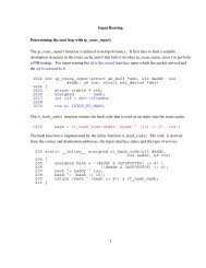
R4300i Product Information - MIPS Technologies, Inc.
R4300i Product Information - MIPS Technologies, Inc.
R4300i Product Information - MIPS Technologies, Inc.

Create successful ePaper yourself
Turn your PDF publications into a flip-book with our unique Google optimized e-Paper software.
<strong>R4300i</strong> MICROPROCESSOR<br />
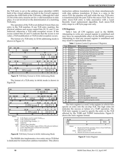
the TLB entry is set or the address space identifier (ASID)<br />
field of the virtual address (as held in the EntryHi register)<br />
matches the ASID field of the TLB entry. Although the valid<br />
(V) bit of the entry must be set for a valid translation to take<br />
place, it is not involved in the determination of a matching<br />
TLB entry.<br />
The operation of the TLB is not defined if more than one<br />
entry in the TLB matches. If one TLB entry matches, the<br />
physical address and access control bits (N, D, and V) are<br />
retrieved; otherwise a TLB refill exception occurs. If the<br />
access control bits (D and V) indicate that the access is not<br />
valid, a TLB modification or TLB invalid exception occurs.<br />
The format of a TLB entry in 32-bit addressing mode is<br />
shown in Figure 19.<br />
127 121 120 109 108 96<br />
- MASK<br />
-<br />
7<br />
12<br />
13<br />
95 77 76 75 72 71 64<br />
VPN2 G - ASID<br />
19<br />
1 4 8<br />
63 57 56 38 37 35 34 33 32<br />
- PFN (even) C D V -<br />
6<br />
19<br />
3 1 1 1<br />
31 25 24 6 5 3 2 1 0<br />
- PFN (odd) C D V -<br />
6<br />
19<br />
3 1 1 1<br />
Figure 19 TLB Entry Format in 32-bit Addressing Mode<br />
The format of a TLB entry in 64-bit mode is shown in<br />
Figure 20.<br />
255<br />
217 216 205 204 192<br />
- MASK -<br />
39 12 13<br />
191 190 189 168 167<br />
141 140 139 136 135 128<br />
R<br />
VPN2 G - ASID<br />
2 22 27 1 4 8<br />
127<br />
89 88<br />
70 69 67 66 65 64<br />
- PFN (even) C D V -<br />
38<br />
19<br />
3 1 1 1<br />
63<br />
25 24<br />
6 5 3 2 1 0<br />
- PFN (odd) C D V -<br />
38<br />
19<br />
3 1 1 1<br />
Where:<br />
R Is the Region used to match VAddr 63..62<br />
MASK is the comparison MASK<br />
VPN2 is the Virtual Page Number / 2<br />
G Global bit<br />
ASID Address Space Identifier<br />
PFN Physical Page Number (upper 20 bits of the physical address)<br />
C Cache Algorithm (011=cached; 010=uncached)<br />
D If set, page is writable<br />
V If set, entry is valid<br />
Figure 20 TLB Entry Format in 64-bit Addressing Mode<br />
The <strong>R4300i</strong> also implements a two entry micro-TLB that<br />
is dedicated for instruction address translation. This allows<br />
instruction address translation to be done simultaneously<br />
with data address translation. If there is a miss in the<br />
micro-TLB, the pipeline will stall while the new TLB entry<br />
is transferred from the joint TLB to the micro-TLB. The two<br />
entry micro-TLB entry is fully associative with a Least<br />
Recently Used replacement algorithm. Each micro-TLB<br />
entry maps to a 4K byte page size only.<br />
CP0 Registers<br />
Table 1 lists all CP0 registers used in the <strong>R4300i</strong>.<br />
Attempting to write any unused register is undefined and<br />
may have an unpredictable effect on the <strong>R4300i</strong> processor.<br />
Attempting to read any unused register is undefined and<br />
may result in unpredictable data.<br />
Table 1 System Control Coprocessor 0 Registers<br />
Num Mnemonic Descriptions<br />
0 Index Programmable pointer into TLB array<br />
1 Random Random pointer into TLB array<br />
2 EntryLo0 Low half of the TLB entry for even VPN<br />
3 EntryLo1 Low half of the TLB entry for odd VPN<br />
4 Context Pointer to kernel PTE table<br />
5 PageMask TLB page mask<br />
6 Wired Number of wire TLB entries<br />
7 ---- Unused<br />
8 BadVAddr Bad virtual address<br />
9 Count Timer count<br />
10 EntryHi High half of TLB entry<br />
11 Compare Timer compare<br />
12 SR Status register<br />
13 Cause Cause register<br />
14 EPC Exception program counter<br />
15 PRid Processor revision identifier<br />
16 Config Configuration register<br />
17 LLAddr Load linked address<br />
18 WatchLo Memory reference trap address lower bits<br />
19 WatchHi Memory reference trap address upper bits<br />
20 XContext Context register for <strong>MIPS</strong>-III addressing<br />
21-25 ---- Unused<br />
26 PErr Not Used<br />
27 CacheErr Not Used<br />
28 TagLo Cache tag register<br />
29 TagHi Cache tag register (Reserved)<br />
30 ErrorEPC Error exception program counter<br />
31 ---- Unused<br />
The Index register is a read/write register in which 6 bits<br />
specify an entry into the on-chip TLB. The high order bit<br />
indicates the success or failure of a TLBP operation. The<br />
TLB Index register is used to specify the entry in the TLB<br />
affected by the TLBR and TLBWI instructions. Figure 21<br />
shows the Index register format.<br />
31 30 6 5 0<br />
P<br />
0<br />
Index<br />
1<br />
25<br />
6<br />
where:<br />
P Result of last Probe operation. Set to 1 if last TLB Probe<br />
instruction was unsuccessful<br />
index Index to entry in TLB<br />
0 Must be all zeroes on reads and writes<br />
Figure 21 Index Register<br />
10 R4300 Data Sheet, Rev 0.3, April 1997