R4300i Product Information - MIPS Technologies, Inc.
R4300i Product Information - MIPS Technologies, Inc.
R4300i Product Information - MIPS Technologies, Inc.

Create successful ePaper yourself
Turn your PDF publications into a flip-book with our unique Google optimized e-Paper software.
<strong>R4300i</strong> MICROPROCESSOR<br />
any combination of single or double-word data until it is<br />
full, with each write occupying one entry in the buffer. For<br />
data cache block write operations, the flush buffer accepts 2<br />
double-words with 1 address, occupying two entries in the<br />
buffer. It is able to take two block references at a time.<br />
Instruction cache block writes use 4 doublewords with 1<br />
address. Instruction cache block writes occupy the entire<br />
flush buffer. The flush buffer is able to take one read<br />
memory reference at a time.<br />
Address is a 32-bit physical address, and size indicates<br />
the size of data to be transferred out.<br />
During an uncached store, data will be stored in this<br />
buffer until it is taken by the external interface. While data<br />
awaits in this area, processor pipeline continues to execute.<br />
During a load miss or a store miss to a cache line in the<br />
dirty state, a read request for the missing cache line is sent<br />
to the external interface. The dirty data is then stored in the<br />
flush buffer until the requested data is returned from the<br />
external interface. The processor pipeline continues to run<br />
while the flush buffer writes the dirty data to the external<br />
interface.<br />
If the flush buffer is full and the processor attempts a<br />
load or a store which requires external resources, the<br />
processor pipeline will stall until the buffer is emptied.<br />
Figure 17 shows the layout of the flush buffer.<br />
decode signals from the integer unit and interprets them to<br />
determine whether a CP0 register is to be read or written. It<br />
generates control signals for reading and writing TLB and<br />
ITLB entries.<br />
IVA<br />
DVA<br />
DBUS<br />
CACHE DATA<br />
INTERRUPTS<br />
INDEX<br />
ENHI<br />
ENLO<br />
ITLB<br />
TLB<br />
CP0REG<br />
TLBMISS<br />
ADDR CHK<br />
TAG<br />
DATA<br />
CP0CTL<br />
I-PFN<br />
D-PFN<br />
EXCEPTIONS<br />
STATUS<br />
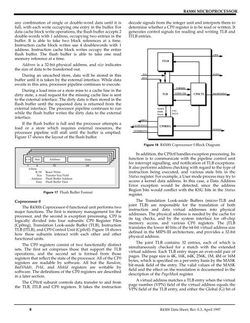
Figure 18 <strong>R4300i</strong> Coprocessor 0 Block Diagram<br />
R/W Size Address Data<br />
1 4 32 64<br />
where:<br />
R/W Read/Write<br />
Size Transfer Size Field<br />
Address Flush Buffer Address<br />
Data Flush Buffer Data<br />
Figure 17 Flush Buffer Format<br />
Coprocessor 0<br />
The <strong>R4300i</strong> Coprocessor-0 functional unit performs two<br />
major functions. The first is memory management for the<br />
processor, and the second is exception processing. CP0 is<br />
logically divided into four subunits: CP0 Register Files<br />
(Cp0reg), Translation Look-aside Buffer (TLB), Instruction<br />
TLB (ITLB), and CP0 Control Unit (Cp0ctl). Figure 18 shows<br />
how these subunits interact with each other and other<br />
functional units.<br />
The CP0 registers consist of two functionally distinct<br />
sets. The first set comprises those that support the TLB<br />
operations, and the second set is formed from those<br />
registers that reflect the state of the processor. All of the CP0<br />
registers are readable by software. All but the Random,<br />
BadVAddr, PrId, and MskId registers are writable by<br />
software. The definitions of the CP0 registers are described<br />
in a later section.<br />
The CP0ctl subunit controls data transfer to and from<br />
the TLB, ITLB and CP0 registers. It takes the instruction<br />
In addition, the CP0ctl handles exception processing. Its<br />
function is to communicate with the pipeline control unit<br />
for interrupt signalling, and notification of TLB exceptions.<br />
It also performs address checking with regard to the type of<br />
instruction being executed, and various state bits in the<br />
Status register. For example, a User mode process may try to<br />
access a kernel data address. In this case, a Data Address<br />
Error exception would be detected, since the address<br />
Region bits would conflict with the KSU bits in the Status<br />
register.<br />
The Translation Look-aside Buffers (micro-TLB and<br />
joint TLB) are responsible for the translation of both<br />
instruction and data virtual addresses into physical<br />
addresses. The physical address is needed by the cache for<br />
its tag checks, and by the system interface for off-chip<br />
memory access, and various CP0 registers. The jTLB<br />
translates the lower 40 bits of the 64-bit virtual address size<br />
defined in the <strong>MIPS</strong>-III architecture, and provides a 32-bit<br />
physical address.<br />
The joint TLB contains 32 entries, each of which is<br />
simultaneously checked for a match with the extended<br />
virtual address. Each TLB entry maps an even-odd pair of<br />
pages. The page size is 4K, 16K, 64K, 256K, 1M, 4M or 16M<br />
bytes, which is specified on a per-entry basis by the MASK<br />
bit-mask field of the entry. The valid values of the MASK<br />
field and the effect on the translation is documented in the<br />
description of the PageMask register.<br />
A virtual address matches a TLB entry when the virtual<br />
page number (VPN) field of the virtual address equals the<br />
VPN field of the TLB entry, and either the Global (G) bit of<br />
9 R4300 Data Sheet, Rev 0.3, April 1997