

Serial Input, 14-Bit/16-Bit DAC AD7849 - Analog Devices
Serial Input, 14-Bit/16-Bit DAC AD7849 - Analog Devices
Serial Input, 14-Bit/16-Bit DAC AD7849 - Analog Devices

You also want an ePaper? Increase the reach of your titles
YUMPU automatically turns print PDFs into web optimized ePapers that Google loves.
<strong>Serial</strong> <strong>Input</strong>,<br />
<strong>14</strong>-<strong>Bit</strong>/<strong>16</strong>-<strong>Bit</strong> <strong>DAC</strong><br />
<strong>AD7849</strong><br />
FEATURES<br />
FUNCTIONAL BLOCK DIAGRAM<br />
<strong>14</strong>-bit/<strong>16</strong>-bit multiplying <strong>DAC</strong><br />
Guaranteed monotonicity<br />
Output control on power-up and power-down internal or<br />
external control<br />
Versatile serial interface<br />
<strong>DAC</strong> clears to 0 V in both unipolar and bipolar output ranges<br />
APPLICATIONS<br />
Industrial process controls<br />
PC analog I/O boards<br />
Instrumentation<br />
V REF+<br />
V REF–<br />
R<br />
R<br />
R<br />
<strong>16</strong>-SEGMENT<br />
SWITCH MATRIX<br />
4<br />
<strong>AD7849</strong><br />
A1<br />
A2<br />
V DD V CC<br />
R<br />
10-BIT/<br />
12-BIT<br />
<strong>DAC</strong><br />
10/<br />
12<br />
<strong>DAC</strong><br />
LATCH<br />
10/<br />
12<br />
INPUT<br />
LATCH<br />
R<br />
A3<br />
G1<br />
LOGIC<br />
CIRCUITRY<br />
VOLTAGE<br />
MONITOR<br />
G2<br />
R OFS<br />
RST IN<br />
V OUT<br />
AGND<br />
RST OUT<br />
INPUT SHIFT REGISTER/<br />
CONTROL LOGIC<br />
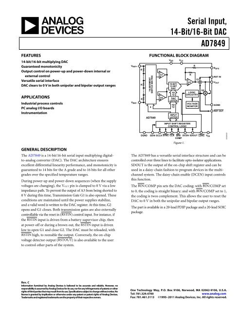
GENERAL DESCRIPTION<br />
The <strong>AD7849</strong> is a <strong>14</strong>-bit/<strong>16</strong>-bit serial input multiplying digitalto-analog<br />
converter (<strong>DAC</strong>). The <strong>DAC</strong> architecture ensures<br />
excellent differential linearity performance, and monotonicity is<br />
guaranteed to <strong>14</strong> bits for the A grade and to <strong>16</strong> bits for all other<br />
grades over the specified temperature ranges.<br />
During power-up and power-down sequences (when the supply<br />
voltages are changing), the VOUT pin is clamped to 0 V via a low<br />
impedance path. To prevent the output of A3 from being shorted to<br />
0 V during this time, Transmission Gate G1 is also opened. These<br />
conditions are maintained until the power supplies stabilize,<br />
and a valid word is written to the <strong>DAC</strong> register. At this time, G2<br />
opens and G1 closes. Both transmission gates are also externally<br />
controllable via the reset in (RSTIN) control input. For instance, if<br />
the RSTIN input is driven from a battery supervisor chip, then<br />
at power-off or during a brown out, the RSTIN input is driven<br />
low to open G1 and close G2. The <strong>DAC</strong> must be reloaded, with<br />
RSTIN high, to reenable the output. Conversely, the on-chip<br />
voltage detector output (RSTOUT) is also available to the user<br />
to control other parts of the system.<br />
DGND<br />
SDIN SCLK SYNC CLR BIN/ DCEN SDOUT L<strong>DAC</strong> V SS<br />
COMP<br />
Figure 1.<br />
The <strong>AD7849</strong> has a versatile serial interface structure and can be<br />
controlled over three lines to facilitate opto-isolator applications.<br />
SDOUT is the output of the on-chip shift register and can be<br />
used in a daisy-chain fashion to program devices in the multichannel<br />
system. The daisy-chain enable (DCEN) input controls<br />
this function.<br />
The BIN/COMP pin sets the <strong>DAC</strong> coding; with BIN/COMP set<br />
to 0, the coding is straight binary; and with BIN/COMP set to 1,<br />
the coding is twos complement. This allows the user to reset the<br />
<strong>DAC</strong> to 0 V in both the unipolar and bipolar output ranges.<br />
The part is available in a 20-lead PDIP package and a 20-lead SOIC<br />
package.<br />
01008-001<br />
Rev. C<br />
Information furnished by <strong>Analog</strong> <strong>Devices</strong> is believed to be accurate and reliable. However, no<br />
responsibility is assumed by <strong>Analog</strong> <strong>Devices</strong> for its use, nor for any infringements of patents or other<br />
rights of third parties that may result from its use. Specifications subject to change without notice. No<br />
license is granted by implication or otherwise under any patent or patent rights of <strong>Analog</strong> <strong>Devices</strong>.<br />
Trademarks and registered trademarks are the property of their respective owners.<br />
One Technology Way, P.O. Box 9106, Norwood, MA 02062-9106, U.S.A.<br />
Tel: 781.329.4700<br />
www.analog.com<br />
Fax: 781.461.3113 ©1995–2011 <strong>Analog</strong> <strong>Devices</strong>, Inc. All rights reserved.
<strong>AD7849</strong><br />
TABLE OF CONTENTS<br />
Features .............................................................................................. 1<br />
Applications....................................................................................... 1<br />
Functional Block Diagram .............................................................. 1<br />
General Description ......................................................................... 1<br />
Revision History ............................................................................... 2<br />
Specifications..................................................................................... 3<br />
Reset Specifications...................................................................... 4<br />
AC Performance Characteristics ................................................ 5<br />
Timing Characteristics ................................................................ 5<br />
Absolute Maximum Ratings............................................................ 6<br />
ESD Caution.................................................................................. 6<br />
Pin Configuration and Function Descriptions............................. 7<br />
Typical Performance Characteristics ..............................................8<br />
Terminology.................................................................................... 10<br />
Circuit Description......................................................................... 11<br />
Digital-to-<strong>Analog</strong> Conversion.................................................. 11<br />
Digital Interface.......................................................................... 12<br />
Applying the <strong>AD7849</strong> ................................................................ 13<br />
Microprocessor Interfacing....................................................... 15<br />
Applications Information .............................................................. 17<br />
Opto-Isolated Interface ............................................................. 17<br />
Outline Dimensions ....................................................................... 18<br />
Ordering Guide .......................................................................... 19<br />
REVISION HISTORY<br />
3/11—Rev. B to Rev. C<br />
Deleted 20-Lead CERDIP (Q-20) Package and<br />
T Version .............................................................................Universal<br />
Updated Format..................................................................Universal<br />
Deleted <strong>AD7849</strong>-to-ADSP-2101/ADSP-2102 Interface Section<br />
and Figure 20; Renumbered Sequentially.................................... 12<br />
Rev. C | Page 2 of 20
<strong>AD7849</strong><br />
SPECIFICATIONS<br />
VDD = <strong>14</strong>.25 V to 15.75 V; VSS = −<strong>14</strong>.25 V to −15.75 V; VCC = 4.75 V to 5.25 V; VOUT loaded with 2 kΩ, 200 pF to 0 V; VREF+ = 5 V; ROFS<br />
connected to 0 V; TA = TMIN to TMAX, unless otherwise noted. Temperature range for A, B, C versions is −40°C to +85°C.<br />
Table 1.<br />
Parameter A Version B Version C Version Unit Test Conditions/Comments<br />
RESOLUTION <strong>14</strong> <strong>16</strong> <strong>16</strong> <strong>Bit</strong>s A version: 1 LSB = 2 (VREF+ − VREF−)/2 <strong>14</strong> ;<br />
B, C versions: 1 LSB = 2 (VREF+ − VREF−)/2 <strong>16</strong><br />
UNIPOLAR OUTPUT<br />
VREF− = 0 V, VOUT = 0 V to 10 V<br />
Relative Accuracy at 25°C ±4 ±6 ±4 LSB typ<br />
TMIN to TMAX ±5 ±<strong>16</strong> ±8 LSB max<br />
Differential Nonlinearity ±0.25 ±0.9 ±0.5 LSB max All grades guaranteed monotonic<br />
over temperature<br />
Gain Error at 25°C ±1 ±4 ±4 LSB typ VOUT load = 10 MΩ<br />
TMIN to TMAX ±4 ±<strong>16</strong> ±<strong>16</strong> LSB max<br />
Offset Error at 25°C ±1 ±4 ±4 LSB typ<br />
TMIN to TMAX ±6 ±24 ±<strong>16</strong> LSB max<br />
Gain Temperature Coefficient 1 ±2 ±2 ±2 ppm FSR/<br />
°C typ<br />
Offset Temperature Coefficient 1 ±2 ±2 ±2 ppm FSR/<br />
°C typ<br />
BIPOLAR OUTPUT<br />
VREF− = 5 V, VOUT = −10 V to +10 V<br />
Relative Accuracy at 25°C ±2 ±3 ±2 LSB typ<br />
TMIN to TMAX ±3 ±8 ±4 LSB max<br />
Differential Nonlinearity ±0.25 ±0.9 ±0.5 LSB max All grades guaranteed monotonic<br />
over temperature<br />
Gain Error at 25°C ±1 ±4 ±4 LSB typ VOUT load = 10 MΩ<br />
TMIN to TMAX ±4 ±<strong>16</strong> ±<strong>16</strong> LSB max<br />
Offset Error at 25°C ±0.5 ±2 ±2 LSB typ<br />
TMIN to TMAX ±3 ±12 ±8 LSB max<br />
Bipolar Zero Error at 25°C ±0.5 ±2 ±2 LSB typ<br />
TMIN to TMAX ±4 ±12 ±8 LSB max<br />
Gain Temperature Coefficient 1 ±2 ±2 ±2 ppm FSR/<br />
°C typ<br />
Offset Temperature Coefficient 1 ±2 ±2 ±2 ppm FSR/<br />
°C typ<br />
Bipolar Zero Temperature<br />
Coefficient1<br />
±2 ±2 ±2 ppm FSR/<br />
°C typ<br />
REFERENCE INPUT<br />
<strong>Input</strong> Resistance 25 25 25 kΩ min Resistance from VREF+ to VREF−<br />
43 43 43 kΩ max Typically 34 kΩ<br />
VREF+ Range<br />
VSS + 6 to<br />
VDD − 6<br />
VSS + 6 to<br />
VDD − 6<br />
VSS + 6 to<br />
VDD − 6<br />
V<br />
VREF− Range<br />
OUTPUT CHARACTERISTICS<br />
Output Voltage Swing<br />
VSS + 6 to<br />
VDD − 6<br />
VSS + 4 to<br />
VDD − 4<br />
VSS + 6 to<br />
VDD − 6<br />
VSS + 4 to<br />
VDD − 4<br />
VSS + 6 to<br />
VDD − 6<br />
VSS + 4 to<br />
VDD − 4<br />
Resistive Load 2 2 2 kΩ min To 0 V<br />
Capacitive Load 200 200 200 pF max To 0 V<br />
Output Resistance 0.3 0.3 0.3 Ω typ<br />
Short-Circuit Current ±25 ±25 ±25 mA typ Voltage range: −10 V to +10 V<br />
V<br />
V max<br />
Rev. C | Page 3 of 20
<strong>AD7849</strong><br />
Parameter A Version B Version C Version Unit Test Conditions/Comments<br />
DIGITAL INPUTS<br />
<strong>Input</strong> High Voltage, VINH 2.4 2.4 2.4 V min<br />
<strong>Input</strong> Low Voltage, VINL 0.8 0.8 0.8 V max<br />
<strong>Input</strong> Current, IINH ±10 ±10 ±10 μA max<br />
<strong>Input</strong> Capacitance, CIN 10 10 10 pF max<br />
DIGITAL OUTPUTS<br />
Output Low Voltage, VOL 0.4 0.4 0.4 V max ISINK = 1.6 mA<br />
Output High Voltage, VOH 4.0 4.0 4.0 V min ISOURCE = 400 μA<br />
Floating State Leakage Current ±10 ±10 ±10 μA max<br />
Floating State Output<br />
10 10 10 pF max<br />
Capacitance<br />
POWER REQUIREMENTS 2<br />
VDD <strong>14</strong>.25/15.75 <strong>14</strong>.25/15.75 <strong>14</strong>.25/15.75 V min/V max<br />
VSS −<strong>14</strong>.25/−15.75 −<strong>14</strong>.25/−15.75 −<strong>14</strong>.25/−15.75 V min/V max<br />
VCC 4.75/5.25 4.75/5.25 4.75/5.25 V min/V max<br />
IDD 5 5 5 mA max VOUT unloaded, VINH = VDD – 0.1 V,<br />
VINL = 0.1 V<br />
ISS 5 5 5 mA max VOUT unloaded, VINH = VDD – 0.1 V,<br />
VINL = 0.1 V<br />
ICC 2.5 2.5 2.5 mA max VINH = VDD – 0.1 V, VINL = 0.1 V<br />
Power Supply Sensitivity 3 0.4 1.5 1.5 LSB/V max<br />
Power Dissipation 100 100 100 mW typ VOUT unloaded<br />
1<br />
Guaranteed by design and characterization, not production tested.<br />
2<br />
The <strong>AD7849</strong> is functional with power supplies of ±12 V. See the Typical Performance Characteristics section.<br />
3<br />
Sensitivity of gain error, offset error, and bipolar zero error to VDD, VSS variations.<br />
RESET SPECIFICATIONS<br />
These specifications apply when the device goes into reset mode during power-up or power-down sequence. VOUT unloaded.<br />
Table 2.<br />
Parameter All Versions Unit Test Conditions/Comments<br />
VA, 1 Low Threshold Voltage for VDD, VSS 1.2 V max This is the lower VDD/VSS threshold voltage for the reset function.<br />
0 V typ Above this, the reset is activated.<br />
VB, High Threshold Voltage for VDD, VSS 9.5 V max This is the higher VDD/VSS threshold voltage for the reset function.<br />
6.4 V min Below this, the reset is activated. Typically, 8 V.<br />
VC, Low Threshold Voltage for VCC 1 V max This is the lower VCC threshold voltage for the reset function.<br />
0 V typ Above this, the reset is activated.<br />
VD, High Threshold Voltage for VCC 4 V max This is the higher VCC threshold voltage for the reset function.<br />
2.5 V min Below this, the reset is activated. Typically, 3 V.<br />
G2 RON 1 kΩ typ On resistance of G2; VDD = 2 V; VSS = −2 V; IG2 = 1 mA.<br />
1<br />
A pull-down resistor (65 kΩ) on VOUT maintains 0 V output when VDD/VSS is below VA.<br />
Rev. C | Page 4 of 20
<strong>AD7849</strong><br />
AC PERFORMANCE CHARACTERISTICS<br />
These characteristics are included for design guidance and are no subject to test. VREF+ = 5 V; VDD = <strong>14</strong>.25 V to 15.75 V; VSS = −<strong>14</strong>.25 V to<br />
−15.75 V; VCC = 4.75 V to 5.25 V; ROFS connected to 0 V.<br />
Table 3.<br />
Parameter A, B, C Versions Unit Test Conditions/Comments<br />
DYNAMIC PERFORMANCE<br />
Output Settling Time 1 7 μs typ To 0.006% FSR. VOUT loaded. VREF− = 0 V.<br />
10 μs typ To 0.003% FSR. VOUT loaded. VREF− = −5 V.<br />
Slew Rate 4 V/μs typ<br />
Digital-to-<strong>Analog</strong> Glitch Impulse 250 nV-sec typ <strong>DAC</strong> alternatively loaded with 00 … 00 and<br />
111 … 11. VOUT loaded. L<strong>DAC</strong> permanently low.<br />
BIN/COMP set to 1. VREF− = −5 V.<br />
150 nV-sec typ L<strong>DAC</strong> frequency = 100 kHz.<br />
AC Feedthrough 1 mV p-p typ VREF− = 0 V, VREF+ = 1 V rms, 10 kHz sine wave.<br />
<strong>DAC</strong> loaded with all 0s. BIN/COMP set to 0.<br />
Digital Feedthrough 5 nV-sec typ <strong>DAC</strong> alternatively loaded with all 1s and 0s.<br />
SYNC high.<br />
Output Noise Voltage Density, 1 kHz to 100 kHz 80 nV/√Hz typ Measured at VOUT. VREF+ = VREF− = 0 V.<br />
BIN/COMP set to 0.<br />
1<br />
L<strong>DAC</strong> = 0. Settling time does not include deglitching time of 5 μs (typical).<br />
TIMING CHARACTERISTICS<br />
VDD = <strong>14</strong>.25 V to 15.75 V; VSS = −<strong>14</strong>.25 V to −15.75 V; VCC = 4.75 V to 5.25 V; RL = 2 kΩ, CL = 200 pF. All specifications TMIN to TMAX,<br />
unless otherwise noted. Guaranteed by characterization. All input signals are specified tr = tf = 5 ns (10% to 90% of 5 V and timed from a<br />
voltage level of 1.6 V.<br />
Table 4.<br />
Parameter Limit at 25°C (All Versions) Limit at TMIN, TMAX (All Versions) Unit Test Conditions/Comments<br />
t1 1 200 200 ns min SCLK cycle time<br />
t2 50 50 ns min SYNC-to-SCLK setup time<br />
t3 70 70 ns min SYNC-to-SCLK hold time<br />
t4 10 10 ns min Data setup time<br />
t5 40 40 ns min Data hold time<br />
t6 2 80 80 ns max SCLK falling edge to SDO valid<br />
t7 80 80 ns min L<strong>DAC</strong>, CLR pulse width<br />
tr 30 30 μs max Digital input rise time<br />
tf 30 30 μs max Digital input fall time<br />
1<br />
SCLK mark/space ratio range is 40/60 to 60/40.<br />
2<br />
SDO load capacitance is 50 pF.<br />
Rev. C | Page 5 of 20
<strong>AD7849</strong><br />
ABSOLUTE MAXIMUM RATINGS<br />
TA = 25°C, unless otherwise noted.<br />
Table 5.<br />
Parameter<br />
Rating<br />
VDD to DGND<br />
−0.4 V to +17 V<br />
VCC to DGND 1<br />
−0.4 V, VDD + 0.4 V or<br />
+7 V (whichever is<br />
lower)<br />
VSS to DGND<br />
−0.4 V to −17 V<br />
VREF+ to DGND<br />
VDD + 0.4 V, VSS − 0.4 V<br />
VREF− to DGND<br />
VDD + 0.4 V, VSS − 0.4 V<br />
VOUT to DGND 2<br />
VDD + 0.4 V, VSS − 0.4 V<br />
or ±10 V (whichever is<br />
lower)<br />
ROFS to DGND<br />
VDD + 0.4 V, VSS − 0.4 V<br />
Digital <strong>Input</strong> Voltage to DGND<br />
−0.4 V to VCC + 0.4 V<br />
<strong>Input</strong> Current to any Pin Except Supplies 3 ±10 mA<br />
Operating Temperature Range<br />
−40°C to +85°C<br />
Storage Temperature Range<br />
−65°C to +150°C<br />
Junction Temperature 150°C<br />
20-Lead PDIP<br />
Power Dissipation<br />
875 mW<br />
θJA Thermal Impedance<br />
102°C/W<br />
Lead Temperature (Soldering, 10 sec) 260°C<br />
20-Lead SOIC<br />
Power Dissipation<br />
875 mW<br />
θJA Thermal Impedance<br />
74°C/W<br />
Lead Temperature, Soldering<br />
Vapor Phase (60 sec) 215°C<br />
Infrared (15 sec) 220°C<br />
Stresses above those listed under Absolute Maximum Ratings<br />
may cause permanent damage to the device. This is a stress<br />
rating only; functional operation of the device at these or any<br />
other conditions above those indicated in the operational<br />
section of this specification is not implied. Exposure to absolute<br />
maximum rating conditions for extended periods may affect<br />
device reliability.<br />
ESD CAUTION<br />
1<br />
VCC must not exceed VDD by more than 0.4 V. If it is possible for this to<br />
happen during power-up or power-down (for example, if VCC is greater than<br />
0.4 V while VDD is still 0 V), the following diode protection scheme ensures<br />
protection.<br />
V DD<br />
V CC<br />
SD103C<br />
1N4<strong>14</strong>8 1N5711<br />
1N5712<br />
V DD<br />
V CC<br />
<strong>AD7849</strong><br />
2<br />
VOUT can be shorted to DGND, + 10 V, − 10 V, provided that the power<br />
dissipation of the package is not exceeded.<br />
3<br />
Transient currents of up to 100 mA do not cause SCR latch-up.<br />
01008-002<br />
Rev. C | Page 6 of 20
<strong>AD7849</strong><br />
PIN CONFIGURATION AND FUNCTION DESCRIPTIONS<br />
V REF+ 1<br />
20 R OFS<br />
V REF–<br />
V SS<br />
SYNC<br />
2<br />
3<br />
4<br />
19<br />
18<br />
17<br />
V OUT<br />
NC<br />
V DD<br />
SCLK<br />
<strong>AD7849</strong><br />
5 <strong>16</strong> AGND<br />
V CC 6<br />
TOP VIEW<br />
(Not to Scale) 15 RSTOUT<br />
SDOUT 7 <strong>14</strong> RSTIN<br />
DCEN 8 13 CLR<br />
BIN/COMP 9 12 SDIN<br />
DGND 10 11 L<strong>DAC</strong><br />
NC = NO CONNECT. DO NOT CONNECT TO THIS PIN.<br />
Figure 2. Pin Configuration<br />
01008-003<br />
Table 6. Pin Function Descriptions<br />
Pin No. Mnemonic Description<br />
1 VREF+ VREF+ <strong>Input</strong>. The <strong>DAC</strong> is specified for VREF+ of 5 V. The <strong>DAC</strong> is fully multiplying so that the VREF+ range is +5 V to –5 V.<br />
2 VREF− VREF− <strong>Input</strong>. The <strong>DAC</strong> is specified for VREF− of –5 V. The <strong>DAC</strong> is fully multiplying so that the VREF− range is –5 V to +5 V.<br />
3 VSS Negative supply for the analog circuitry. This is nominally –15 V.<br />
4 SYNC Data Synchronization Logic <strong>Input</strong>. When it goes low, the internal logic is initialized in readiness for a new data-word.<br />
5 SCLK <strong>Serial</strong> Clock Logic <strong>Input</strong>. Data is clocked into the input register on each SCLK falling edge.<br />
6 VCC Positive supply for the digital circuitry. This is nominally 5 V.<br />
7 SDOUT <strong>Serial</strong> Data Output. With DCEN at Logic 1, this output is enabled, and the serial data in the input shift register is<br />
clocked out on each rising edge of SCLK.<br />
8 DCEN Daisy-Chain Enable Logic <strong>Input</strong>. Connect this pin high if a daisy-chain interface is being used; otherwise, this<br />
pin must be connected low.<br />
9 BIN/COMP Logic <strong>Input</strong>. This input selects the data format to be either binary or twos complement. In the unipolar output<br />
range, natural binary format is selected by connecting the input to Logic 0. In the bipolar output range, offset<br />
binary is selected by connecting this input to Logic 0, and twos complement is selected by connecting it to a<br />
Logic 1.<br />
10 DGND Digital Ground. Ground reference point for the on-chip digital circuitry.<br />
11 L<strong>DAC</strong> Load <strong>DAC</strong> Logic <strong>Input</strong>. This input updates the <strong>DAC</strong> output. The <strong>DAC</strong> output is updated on the falling edge of<br />
this signal, or alternatively, if this input is permanently low, an automatic update mode is selected where the<br />
<strong>DAC</strong> is updated on the <strong>16</strong>th falling SCLK edge.<br />
12 SDIN <strong>Serial</strong> Data <strong>Input</strong>. The <strong>16</strong>-bit serial data-word is applied to this input.<br />
13 CLR Clear Logic <strong>Input</strong>. Taking this input low sets VOUT to 0 V in both the unipolar output range and the bipolar twos<br />
complement output range. It sets VOUT to VREF– in the offset binary bipolar output range.<br />
<strong>14</strong> RSTIN Reset Logic <strong>Input</strong>. This input allows external access to the internal reset logic. Applying Logic 0 to this input,<br />
resets the <strong>DAC</strong> output to 0 V. In normal operation, it should be tied to Logic 1.<br />
15 RSTOUT Reset Logic Output. This is the output from the on-chip voltage monitor used in the reset circuit. It can be used<br />
to control other system components, if desired.<br />
<strong>16</strong> AGND This is the analog ground for the device. It is the point to which the output gets shorted in reset mode.<br />
17 VDD Positive Supply for the <strong>Analog</strong> Circuitry. This is 15 V nominal.<br />
18 NC No Connect. Leave unconnected.<br />
19 VOUT <strong>DAC</strong> Output Voltage Pin.<br />
20 ROFS <strong>Input</strong> to Summing Resistor of <strong>DAC</strong> Output Amplifier. This is used to select the output voltage ranges. Also, see<br />
Figure 20 to Figure 23 in the Applying the <strong>AD7849</strong> section.<br />
Rev. C | Page 7 of 20
<strong>AD7849</strong><br />
TYPICAL PERFORMANCE CHARACTERISTICS<br />
V REF+ 1<br />
V OUT 4<br />
C1 FREQ<br />
9.9942kHz<br />
C1 RMS<br />
728mV<br />
C4 RMS<br />
556µV<br />
V OUT (mV p-p)<br />
7<br />
6<br />
5<br />
4<br />
3<br />
2<br />
V DD =+15V<br />
V SS = –15V<br />
V REF+ =1Vrms<br />
V REF– =0V<br />
1<br />
CH1 1.00V<br />
CH4 1.00mV<br />
M 20.0µs CH1<br />
Figure 3. AC Feedthrough<br />
–300mV<br />
01008-004<br />
0<br />
100 1k<br />
10k<br />
100k<br />
1M<br />
FREQUENCY (Hz)<br />
Figure 6. AC Feedthrough vs. Frequency<br />
01008-007<br />
SYNC 1<br />
SDIN 2<br />
V OUT<br />
4<br />
C4 AREA<br />
247.964nV S<br />
L<strong>DAC</strong><br />
1<br />
SDIN 2<br />
4<br />
V OUT<br />
CH4 50.0mV<br />
CH1 5.00V<br />
CH2 5.00V<br />
CH4 200mV<br />
M 1.00µs CH1 3.7V<br />
Figure 4. Digital-to-<strong>Analog</strong> Glitch Impulse Without Internal Deglitcher<br />
22<br />
01008-005<br />
CH1 5.00V CH2 5.00V M 5.00µs CH1 –2.3V<br />
Figure 7. Digital-to-<strong>Analog</strong> Glitch Impulse With Internal Deglitcher<br />
01008-008<br />
20<br />
18<br />
V REF+<br />
1<br />
C1 p-p<br />
10.4V<br />
<strong>16</strong><br />
V OUT (V p-p)<br />
<strong>14</strong><br />
12<br />
10<br />
8<br />
6<br />
V DD =+15V<br />
V SS =–15V<br />
4<br />
V REF+ =±5SINEWAVE<br />
V REF– =0V<br />
2<br />
GAIN = 2<br />
100 1k 10k 100k<br />
1M<br />
FREQUENCY (Hz)<br />
Figure 5. Large Signal Frequency Response<br />
01008-006<br />
V OUT<br />
2<br />
CH1 10.0V<br />
CH2 20.0V M 2.5µs CH1 –400mV<br />
Figure 8. Pulse Response (Large Signal)<br />
C2 p-p<br />
20.8V<br />
C2 RISE<br />
2.79230µs<br />
C2 FALL<br />
3.20385µs<br />
01008-009<br />
Rev. C | Page 8 of 20
<strong>AD7849</strong><br />
V REF+<br />
1<br />
C1 p-p<br />
104mV<br />
V DD<br />
1<br />
C1 RISE<br />
3.808ms<br />
2 V OUT<br />
CH2 200mV M 2.00µs CH1 –10mV<br />
CH1<br />
100mV<br />
Figure 9. Pulse Response (Small Signal)<br />
C2 p-p<br />
2<strong>16</strong>mV<br />
C2 RISE<br />
458ns<br />
C2 FALL<br />
452.4ns<br />
01008-010<br />
V OUT<br />
2<br />
L<strong>DAC</strong><br />
3<br />
CH1 10.0V<br />
CH3 5.0V<br />
CH2 10.0V M 10.0ms CH1 7.8mV<br />
Figure 12. Turn-On Characteristics<br />
C2 RISE<br />
8µs<br />
01008-013<br />
2.0<br />
1.5<br />
T A = 25°C<br />
V REF+ =5V<br />
V REF– =0V<br />
GAIN = 1<br />
V DD<br />
7.8V<br />
C1 FALL<br />
4.7621ms<br />
1<br />
INL (LSB)<br />
1.0<br />
0.5<br />
V OUT<br />
2<br />
0<br />
11.00 12.25<br />
13.50 <strong>14</strong>.75<br />
V DD /V SS (V)<br />
<strong>16</strong>.00<br />
01008-011<br />
CH1 10.0V<br />
CH2 10.0V M 1.00ms CH1 7.8mV<br />
01008-0<strong>14</strong><br />
Figure 10. Typical Integral Nonlinearity vs. Supplies<br />
Figure 13. Turn-Off Characteristics<br />
0.500<br />
0.375<br />
T A = 25°C<br />
V REF+ =5V<br />
V REF– =0V<br />
GAIN = 1<br />
DNL (LSB)<br />
0.250<br />
0.125<br />
0<br />
11 12 13 <strong>14</strong> 15 <strong>16</strong><br />
V DD /V SS (V)<br />
Figure 11. Typical Differential Nonlinearity vs. Supplies<br />
01008-012<br />
Rev. C | Page 9 of 20
<strong>AD7849</strong><br />
TERMINOLOGY<br />
Least Significant <strong>Bit</strong><br />
This is the analog weighting of 1 bit of the digital word in a<br />
<strong>DAC</strong>. For the B version and the C versions, 1 LSB = (VREF+ −<br />
VREF−)/2 <strong>16</strong> . For the A version, 1 LSB = (VREF+ − VREF−)/2 <strong>14</strong> .<br />
Relative Accuracy<br />
Relative accuracy or endpoint nonlinearity is a measure of the<br />
maximum deviation from a straight line passing through the<br />
endpoints of the <strong>DAC</strong> transfer function. It is measured after<br />
adjusting for both endpoints (that is, offset and gain errors are<br />
adjusted out) and is normally expressed in least significant bits<br />
or as a percentage of full-scale range.<br />
Differential Nonlinearity<br />
Differential nonlinearity is the difference between the measured<br />
change and the ideal change between any two adjacent codes. A<br />
specified differential nonlinearity of less than ±1 LSB over the<br />
operating temperature range ensures monotonicity.<br />
Gain Error<br />
Gain error is a measure of the output error between an ideal<br />
<strong>DAC</strong> and the actual device output with all 1s loaded after offset<br />
error has been adjusted out. Gain error is adjustable to zero<br />
with an external potentiometer.<br />
Offset Error<br />
This is the error present at the device output with all 0s loaded<br />
in the <strong>DAC</strong>. It is due to the op amp input offset voltage and bias<br />
current and the <strong>DAC</strong> leakage current.<br />
Bipolar Zero Error<br />
When the <strong>AD7849</strong> is connected for bipolar output and (100 …<br />
000) is loaded to the <strong>DAC</strong>, the deviation of the analog output<br />
from the ideal midscale of 0 V is called the bipolar zero error.<br />
Digital-to-<strong>Analog</strong> Glitch Impulse<br />
This is the amount of charge injected from the digital inputs to<br />
the analog output when the inputs change state. Normally, this<br />
is specified as the area of the glitch in nV-secs.<br />
Multiplying Feedthrough Error<br />
This is an ac error due to capacitive feedthrough from either of<br />
the VREF terminals to VOUT when the <strong>DAC</strong> is loaded with all 0s.<br />
Digital Feedthrough<br />
When the <strong>DAC</strong> is not selected (SYNC is held high), high<br />
frequency logic activity on the digital inputs is capacitively<br />
coupled through the device to show up as noise on the VOUT pin.<br />
This noise is digital feedthrough.<br />
Rev. C | Page 10 of 20
<strong>AD7849</strong><br />
CIRCUIT DESCRIPTION<br />
DIGITAL-TO-ANALOG CONVERSION<br />
Figure 15 shows the digital-to-analog section of the <strong>AD7849</strong>. There<br />
are three on-chip <strong>DAC</strong>s, each of which has its own buffer amplifier.<br />
<strong>DAC</strong>1 and <strong>DAC</strong>2 are 4-bit <strong>DAC</strong>s. They share a <strong>16</strong>-resistor string,<br />
but they have their own analog multiplexers. The voltage reference<br />
is applied to the resistor string. <strong>DAC</strong>3 is a 12-bit voltage mode<br />
<strong>DAC</strong> with its own output stage.<br />
The four MSBs of the <strong>16</strong>-bit digital input code drive <strong>DAC</strong>1 and<br />
<strong>DAC</strong>2, while the 12 LSBs control <strong>DAC</strong>3. Using <strong>DAC</strong>1 and <strong>DAC</strong>2,<br />
the MSBs select a pair of adjacent nodes on the resistor string<br />
and present that voltage to the positive and negative inputs of<br />
<strong>DAC</strong>3. This <strong>DAC</strong> interpolates between these two voltages to<br />
produce the analog output voltage.<br />
To prevent nonmonotonicity in the <strong>DAC</strong> due to amplifier offset<br />
voltages, <strong>DAC</strong>1 and <strong>DAC</strong>2 leap-frog along the resistor string.<br />
For example, when switching from Segment 1 to Segment 2, <strong>DAC</strong>1<br />
switches from the bottom of Segment 1 to the top of Segment 2<br />
while <strong>DAC</strong> 2 remains connected to the top of Segment 1. The<br />
code driving <strong>DAC</strong>3 is automatically complemented to compensate<br />
for the inversion of its inputs. This means that any linearity<br />
effects due to amplifier offset voltages remain unchanged when<br />
switching from one segment to the next, and <strong>16</strong>-bit monotonicity is<br />
ensured if <strong>DAC</strong>3 is monotonic. Therefore, 12-bit resistor matching<br />
in <strong>DAC</strong>3 guarantees overall <strong>16</strong>-bit monotonicity. This is much<br />
more achievable than the <strong>16</strong>-bit matching that a conventional<br />
R-2R structure would need.<br />
Output Stage<br />
The output stage of the <strong>AD7849</strong> is shown in Figure <strong>14</strong>. It is capable<br />
of driving a 2 kΩ load in parallel with 200 pF. The feedback and<br />
offset resistors allow the output stage to be configured for gains of<br />
1 or 2. Additionally, the offset resistor can be used to shift the<br />
output range. The <strong>AD7849</strong> has a special feature to ensure output<br />
stability during power-up and power-down sequences. This feature<br />
is available for control applications where actuators must not be<br />
allowed to move in an uncontrolled fashion.<br />
<strong>DAC</strong> 3<br />
R OFS<br />
R<br />
10kΩ<br />
ONE-SHOT<br />
L<strong>DAC</strong><br />
R<br />
10kΩ<br />
G3<br />
C1<br />
LOGIC<br />
CIRCUITRY<br />
VOLTAGE<br />
MONITOR<br />
RSTIN<br />
G1<br />
Figure <strong>14</strong>. Output Stage<br />
G2<br />
V OUT<br />
AGND<br />
RSTOUT<br />
When the supply voltages are changing, the VOUT pin is clamped<br />
to 0 V via a low impedance path. To prevent the output of A3<br />
from being shorted to 0 V during this time, Transmission Gate G1<br />
is opened. These conditions are maintained until the power<br />
supplies stabilize, and a valid word is written to the <strong>DAC</strong> register.<br />
At this time, G2 opens and G1 closes. Both transmission gates<br />
are also externally controllable via the reset in (RSTIN) control<br />
input. For instance, if the RSTIN input is driven from a battery<br />
supervisor chip, then at power-off or during a brownout, the<br />
RSTIN input will be driven low to open G1 and closeG2. The<br />
<strong>DAC</strong> has to be reloaded, with RSTIN high, to reenable the output.<br />
Conversely, the on-chip voltage detector output (RSTOUT) is<br />
also available to the user to control other parts of the system.<br />
The <strong>AD7849</strong> output buffer is configured as a track-and-hold<br />
amplifier. Although normally tracking its input, this amplifier<br />
isplaced in hold mode for approximately 5 μs after the leading<br />
edge of L<strong>DAC</strong>. This short state keeps the <strong>DAC</strong> output at its<br />
previous voltage while the <strong>AD7849</strong> is internally changing to its<br />
new value. therefore, any glitches that occur in the transition are<br />
not seen at the output. In systems where L<strong>DAC</strong> is permanently<br />
low, deglitching is not in operation.<br />
01008-015<br />
V REF+<br />
R<br />
<strong>DAC</strong> 1<br />
S1<br />
S3<br />
S15<br />
R<br />
R<br />
<strong>DAC</strong> 2<br />
S2<br />
S4<br />
S<strong>14</strong><br />
A1<br />
<strong>DAC</strong> 3<br />
10-BIT/12-BIT<br />
<strong>DAC</strong><br />
OUTPUT<br />
STAGE<br />
S17<br />
R<br />
S<strong>16</strong><br />
10/12<br />
R<br />
V REF–<br />
DB15 TO DB12<br />
R<br />
DB15 TO DB12<br />
A2<br />
01008-0<strong>16</strong><br />
Figure 15. Digital-to-<strong>Analog</strong> Conversion<br />
Rev. C | Page 11 of 20
<strong>AD7849</strong><br />
t 1<br />
SCLK<br />
SYNC<br />
t 2 t 3<br />
BIN/COMP<br />
t 4<br />
t 5<br />
t 7<br />
SDIN<br />
(<strong>AD7849</strong>B/C)<br />
DB15<br />
t 4<br />
t 5<br />
DB0<br />
SDIN<br />
(<strong>AD7849</strong>A)<br />
DB13<br />
DB0<br />
L<strong>DAC</strong>, CLR<br />
NOTES<br />
1. DCEN IS TIED PERMANENTLY LOW.<br />
Figure <strong>16</strong>. Timing Diagram (Standalone Mode)<br />
01008-017<br />
DIGITAL INTERFACE<br />
The <strong>AD7849</strong> contains an input serial-to-parallel shift register and a<br />
<strong>DAC</strong> latch. A simplified diagram of the input loading circuitry is<br />
shown in Figure <strong>16</strong>. <strong>Serial</strong> data on the SDIN input is loaded to<br />
the input register under control of DCEN, SYNC and SCLK.<br />
When a complete word is held in the shift register, it can then be<br />
loaded into the <strong>DAC</strong> latch under control of L<strong>DAC</strong>. Only the data<br />
in the <strong>DAC</strong> latch determines the analog output on the <strong>AD7849</strong>.<br />
The daisy-chain enable (DCEN) input is used to select either the<br />
standalone mode or the daisy-chain mode. The loading format<br />
is slightly different depending on which mode is selected.<br />
<strong>Serial</strong> Data Loading Format (Standalone Mode)<br />
When DCEN is at Logic 0, standalone mode is selected. In this<br />
mode, a low SYNC input provides the frame synchronization<br />
signal that tells the <strong>AD7849</strong> that valid serial data on the SDIN<br />
input is available for the next <strong>16</strong> falling edges of SCLK. An internal<br />
counter/decoder circuit provides a low gating signal so that only<br />
<strong>16</strong> data bits are clocked into the input shift register. After <strong>16</strong> SCLK<br />
pulses, the internal gating signal goes inactive (high), thus locking<br />
out any further clock pulses. Therefore, either a continuous clock<br />
or a burst clock source can be used to clock in data.<br />
The SYNC input is taken high after the complete <strong>16</strong>-bit word is<br />
loaded in.<br />
The B version and C version are <strong>16</strong>-bit resolution <strong>DAC</strong>s and have a<br />
straight <strong>16</strong>-bit load format, with the MSB (DB15) being loaded<br />
first. The A version is a <strong>14</strong>-bit <strong>DAC</strong>; however, the loading structure<br />
is still <strong>16</strong> bit. The MSB (DB13) is loaded first, and the final two<br />
bits of the <strong>16</strong>-bit stream must be 0s.<br />
The <strong>DAC</strong> latch, and hence the analog output, can be updated in<br />
two ways. The status of the L<strong>DAC</strong> input is examined after SYNC<br />
is taken low. Depending on its status, one of two update modes<br />
is selected.<br />
If L<strong>DAC</strong> = 0, then automatic update mode is selected. In this mode,<br />
the <strong>DAC</strong> latch and analog output are updated automatically when<br />
the last bit in the serial data stream is clocked in. The update<br />
thus takes place on the <strong>16</strong>th falling SCLK edge.<br />
If L<strong>DAC</strong> = 1, then automatic update mode is disabled. The <strong>DAC</strong><br />
latch update and output update are now separate. The <strong>DAC</strong> latch is<br />
updated on the falling edge of L<strong>DAC</strong>. However, the output update<br />
is delayed for a further 5 μs by means of an internal track-and-hold<br />
amplifier in the output stage. This function results in a lower<br />
digital-to-analog glitch impulse at the <strong>DAC</strong> output. Note that<br />
the L<strong>DAC</strong> input must be taken back high again before the next<br />
data transfer is initiated.<br />
DCEN<br />
SYNC<br />
SCLK<br />
SDIN<br />
L<strong>DAC</strong><br />
CLR<br />
RESET EN<br />
÷<strong>16</strong><br />
COUNTER/<br />
DECODER<br />
AUTO-UPDATE<br />
CIRCUITRY<br />
GATED<br />
SIGNAL<br />
GATED<br />
SCLK<br />
INPUT<br />
SHIFT REGISTER<br />
(<strong>16</strong> BITS)<br />
<strong>DAC</strong> LATCH<br />
(<strong>14</strong>/<strong>16</strong> BITS)<br />
Figure 17. Simplified Loading Structure<br />
SDOUT<br />
01008-018<br />
Rev. C | Page 12 of 20
t 4<br />
t 5<br />
<strong>AD7849</strong><br />
t 1<br />
t 3<br />
SCLK<br />
SYNC<br />
t 2<br />
BIN/COMP<br />
SDIN<br />
(<strong>AD7849</strong>B/C)<br />
DB15 (N)<br />
DB0 (N)<br />
DB15<br />
(N + 1)<br />
DB0<br />
(N + 1)<br />
t 6<br />
SDOUT<br />
(<strong>AD7849</strong>B/C)<br />
DB15 (N)<br />
t 4<br />
t 5<br />
DB0 (N)<br />
SDIN<br />
(<strong>AD7849</strong>A)<br />
DB13 (N)<br />
DB0 (N)<br />
DB13<br />
(N + 1)<br />
DB0<br />
(N + 1)<br />
SDOUT<br />
(<strong>AD7849</strong>A)<br />
t 6<br />
DB13 (N)<br />
DB0 (N)<br />
L<strong>DAC</strong>, CLR<br />
NOTES<br />
1. DCEN IS TIED PERMANENTLY HIGH.<br />
<strong>Serial</strong> Data Loading Format (Daisy-Chain Mode)<br />
By connecting DCEN high, daisy-chain mode is enabled. This<br />
mode of operation is designed for multi<strong>DAC</strong> systems where<br />
several <strong>AD7849</strong>s can be connected in cascade. In this mode, the<br />
internal gating circuitry on SCLK is disabled, and a serial data<br />
output facility is enabled. The internal gating signal is permanently<br />
active (low) so that the SCLK signal is continuously applied to<br />
the input shift register when SYNC is low. The data is clocked<br />
into the register on each falling SCLK edge after SYNC goes low. If<br />
more than <strong>16</strong> clock pulses are applied, the data ripples out of the<br />
shift register and appears on the SDOUT line. By connecting this<br />
line to the SDIN input on the next <strong>AD7849</strong> in the chain, a<br />
multi<strong>DAC</strong> interface can be constructed. Sixteen SCLK pulses<br />
are required for each <strong>DAC</strong> in the system. Therefore, the total<br />
number of clock cycles must equal <strong>16</strong> × N, where N is the total<br />
number of devices in the chain. When the serial transfer to all<br />
devices is complete, SYNC is taken high, which prevents any<br />
further data from being clocked into the input register.<br />
A continuous SCLK source can be used if SYNC is held low for<br />
the correct number of clock cycles. Alternatively, a burst clock<br />
containing the exact number of clock cycles can be used and<br />
SYNC taken high some time later.<br />
When the transfer to all input registers is complete, a common<br />
L<strong>DAC</strong> signal updates all <strong>DAC</strong> latches with the data in each input<br />
register. All analog outputs are therefore updated simultaneously,<br />
5 μs after the falling edge of L<strong>DAC</strong>.<br />
Figure 18. Timing Diagram (Daisy-Chain Mode)<br />
Clear Function (CLR)<br />
The clear function bypasses the input shift register and loads<br />
the <strong>DAC</strong> latch with all 0s. It is activated by taking CLR low. In<br />
all ranges, except the offset binary bipolar range (–5 V to +5 V),<br />
the output voltage is reset to 0 V. In the offset binary bipolar<br />
range, the output is set to VREF–. This clear function is distinct and<br />
separate from the automatic power-on reset feature of the device.<br />
APPLYING THE <strong>AD7849</strong><br />
Power Supply Sequencing and Decoupling<br />
In the <strong>AD7849</strong>, VCC should not exceed VDD by more than 0.4 V.<br />
If this happens, then an internal diode is turned on, and it produces<br />
latch-up in the device. Care should be taken to employ the<br />
following power supply sequence: VDD, VSS, and then VCC. In<br />
systems where it is possible to have an incorrect power sequence<br />
(for example, if VCC is greater than 0.4 V while VDD is still 0 V),<br />
the circuit shown in Figure 19 can be used to ensure that the<br />
Absolute Maximum Ratings are not exceeded.<br />
1N4<strong>14</strong>8<br />
V DD<br />
SD103C<br />
1N5711<br />
1N5712<br />
t 7<br />
V CC<br />
V DD<br />
<strong>AD7849</strong><br />
V CC<br />
Figure 19. Power Supply Protection<br />
01008-020<br />
01008-019<br />
Rev. C | Page 13 of 20
<strong>AD7849</strong><br />
Unipolar Configuration<br />
Figure 20 shows the <strong>AD7849</strong> in the unipolar binary circuit<br />
configuration. The <strong>DAC</strong> is driven by the AD586, 5 V reference.<br />
Because ROFS is tied to 0 V, the output amplifier has a gain of ×2,<br />
and the output range is 0 V to 10 V. If a 0 V to 5 V range is<br />
required, ROFS should be tied to VOUT, configuring the output<br />
stage for a gain of ×1. Table 7 gives the code table for the circuit<br />
shown in Figure 20.<br />
C1<br />
1nF<br />
2<br />
8<br />
6<br />
AD586<br />
5<br />
4<br />
SIGNAL GND<br />
R1<br />
10kΩ<br />
+15V +5V<br />
V DD<br />
V CC<br />
V<br />
V OUT<br />
OUT<br />
(0V TO 10V)<br />
V REF+ R OFS<br />
<strong>AD7849</strong>*<br />
AGND<br />
V REF– DGND<br />
V SS<br />
–15V<br />
*ADDITIONAL PINS OMITTED FOR CLARITY.<br />
Figure 20. Unipolar Binary Operation<br />
Table 7. Code Table for Figure 20<br />
Binary Number in <strong>DAC</strong> Latch<br />
MSB LSB <strong>Analog</strong> Output (VOUT)<br />
1111 1111 1111 1111 10 (65,535/65,536) V<br />
1000 0000 0000 0000 10 (32,768/65,536) V<br />
0000 0000 0000 0001 10 (1/65,536) V<br />
0000 0000 0000 0000 0 V<br />
Table 7 assumes a <strong>16</strong>-bit resolution; 1 LSB = 10 V/2 <strong>16</strong> =<br />
10 V/65,536 = 152 μV.<br />
Offset and gain can be adjusted in Figure 20 as follows:<br />
• To adjust offset, disconnect the VREF− input from 0 V, load the<br />
<strong>DAC</strong> with all 0s, and adjust the VREF− voltage until VOUT = 0 V.<br />
• To adjust gain, load the <strong>AD7849</strong> with all 1s and adjust R1<br />
until VOUT = 10 (65,535/65,536) = 9.9998474 V for the <strong>16</strong>-bit,<br />
B and C versions. For the <strong>14</strong>-bit A version, VOUT should be<br />
10 (<strong>16</strong>,383/<strong>16</strong>,384) = 9.9993896 V.<br />
If a simple resistor divider is used to vary the VREF− voltage, it is<br />
important that the temperature coefficients of these resistors<br />
match that of the <strong>DAC</strong> input resistance (−300 ppm/°C). Otherwise,<br />
extra offset errors will be introduced over temperature. Many<br />
circuits do not require these offset and gain adjustments. In<br />
these circuits, R1 can be omitted. Pin 5 of the AD586 may be<br />
left open circuit, and Pin 2 (VREF−) of the <strong>AD7849</strong> tied to 0 V.<br />
01008-021<br />
Bipolar Configuration<br />
Figure 21 shows the <strong>AD7849</strong> set up for ±10 V bipolar operation.<br />
The AD588 provides precision ±5 V tracking outputs that are<br />
fed to the VREF+ and VREF− inputs of the <strong>AD7849</strong>.The code table<br />
for the circuit shown in Figure 21 is shown in Table 8.<br />
Full-scale and bipolar-zero adjustment are provided by varying<br />
the gain and balance on the AD588. R2 varies the gain on the<br />
AD588, while R3 adjusts the +5 V and −5 V outputs together<br />
with respect to ground.<br />
R2<br />
100kΩ<br />
C1<br />
1µF<br />
R3<br />
100kΩ<br />
2<br />
7<br />
3<br />
9<br />
1<br />
AD588<br />
5 <strong>14</strong><br />
10<br />
11<br />
R1<br />
39kΩ<br />
12<br />
*ADDITIONAL PINS OMITTED FOR CLARITY<br />
4<br />
8<br />
6<br />
13<br />
15<br />
<strong>16</strong><br />
+15V +5V<br />
V DD<br />
V REF+<br />
V CC<br />
V OUT<br />
R OFS<br />
<strong>AD7849</strong>*<br />
AGND<br />
V REF– DGND<br />
V SS<br />
–15V<br />
Figure 21. Bipolar ±10 V Operation<br />
V OUT<br />
(–10V TO +10V)<br />
SIGNAL<br />
GND<br />
Table 8. Code Table for Figure 21<br />
Binary Number in <strong>DAC</strong> Latch<br />
MSB LSB <strong>Analog</strong> Output (VOUT)<br />
1111 1111 1111 1111 +10 (32,767/32,768) V<br />
1000 0000 0000 0001 +10 (1/32,768) V<br />
1000 0000 0000 0001 0 V<br />
0111 1111 1111 1111 −10 (1/32,768) V<br />
0000 0000 0000 0000 −10 (32,768/32,768) V<br />
Table 8 assumes a <strong>16</strong>-bit resolution; 1 LSB = 20 V/2 <strong>16</strong> = 305 μV.<br />
For bipolar-zero adjustment on the <strong>AD7849</strong>, load the <strong>DAC</strong> with<br />
100 … 000 and adjust R3 until VOUT = 0 V. Full scale is adjusted<br />
by loading the <strong>DAC</strong> with all 1s and adjusting R2 until VOUT =<br />
9.999694 V.<br />
When bipolar-zero and full-scale adjustment are not needed,<br />
omit R2 and R3, connect Pin 11 to Pin 12 on the AD588 and<br />
leave Pin 5 on the AD588 floating.<br />
If a ±5 V output range is desired with the circuit shown in<br />
Figure 21, tie Pin 20 (ROFS) to Pin 19 (VOUT), thus reducing the<br />
output gain stage to unity and giving an output range of ±5 V.<br />
01008-022<br />
Rev. C | Page <strong>14</strong> of 20
<strong>AD7849</strong><br />
Other Output Voltage Ranges<br />
In some cases, users may require output voltage ranges other than<br />
those already mentioned. One example is systems that need the<br />
output voltage to be a whole number of millivolts (that is,1 mV or<br />
2 mV). If the circuit shown in Figure 22 is used, then the LSB size is<br />
125 μV. This makes it possible to program whole millivolt values at<br />
the output. Table 9 shows the code table for the circuit shown in<br />
Figure 22.<br />
8<br />
1<br />
AD584<br />
4<br />
SIGNAL<br />
GND<br />
R1 8.192V<br />
R2<br />
+15V +5V<br />
V DD<br />
V CC<br />
V<br />
R OFS<br />
REF+<br />
V V OUT OUT<br />
(0V TO 8.192V)<br />
V REF–<br />
<strong>AD7849</strong>*<br />
DGND<br />
AGND<br />
*ADDITIONAL PINS OMITTED FOR CLARITY.<br />
Figure 22. 0 V to 8.192 V Output Range<br />
Table 9. Code Table for Figure 22<br />
Binary Number in <strong>DAC</strong> Latch<br />
MSB LSB <strong>Analog</strong> Output (VOUT)<br />
1111 1111 1111 1111 8.192 V (65,535/65,536) = 8.1919 V<br />
1000 0000 0000 0000 8.192 V (32,768/65,536) = 4.096 V<br />
0000 0000 0000 1000 8.192 V (8/65,536) = 0.001 V<br />
0000 0000 0000 0100 8.192 V (4/65,536) = 0.0005 V<br />
0000 0000 0000 0010 8.192 V (2/65,536) = 0.00025 V<br />
0000 0000 0000 0001 8.192 V (1/65,536) = 0.000125 V<br />
Table 9 assumes a <strong>16</strong>-bit resolution; 1 LSB = 8.192 V/2 <strong>16</strong> = 125 μV.<br />
Generating a ±5 V Output Range from a Single +5 V<br />
Reference<br />
Figure 23 shows how to generate a ±5 V output range when<br />
using a single +5 V reference. VREF− is connected to 0 V, and ROFS<br />
is connected to VREF+. The 5 V reference input is applied to these<br />
pins. With all 0s loaded to the <strong>DAC</strong>, the noninverting terminal<br />
of the output stage amplifier is at 0 V, and VOUT is the inverse of<br />
VREF+. With all 1s loaded to the <strong>DAC</strong>, the noninverting terminal of<br />
the output stage amplifier is 5 V and, therefore, VOUT is also 5 V.<br />
+15V +5V<br />
01008-023<br />
MICROPROCESSOR INTERFACING<br />
Microprocessor interfacing to the <strong>AD7849</strong> is via a serial bus<br />
that uses standard protocol compatible with DSP processors<br />
and microcontrollers. The communications channel requires a<br />
3-wire interface consisting of a clock signal, a data signal, and a<br />
synchronization signal. The <strong>AD7849</strong> requires a <strong>16</strong>-bit data-word<br />
with data valid on the falling edge of SCLK. For all the interfaces,<br />
the <strong>DAC</strong> update can be done automatically when all data is<br />
clocked in, or it can be done under control of L<strong>DAC</strong>.<br />
Figure 24 through Figure 27 show the <strong>AD7849</strong> configured for<br />
interfacing to a number of popular DSP processors and<br />
microcontrollers.<br />
<strong>AD7849</strong>-to-DSP56000 Interface<br />
A serial interface between the <strong>AD7849</strong> and the DSP56000 is<br />
shown in Figure 24. The DSP56000 is configured for normal<br />
mode asynchronous operation with a gated clock. It is also<br />
setup for a <strong>16</strong>-bit word with SCK and SC2 as outputs and the<br />
FSL control bit set to 0. SCK is internally generated on the<br />
DSP56000 and applied to the <strong>AD7849</strong> SCLK input. Data from<br />
the DSP56000 is valid on the falling edge of SCK. The SC2 output<br />
provides the framing pulse for valid data. This line must be<br />
inverted before being applied to the SYNC input of the <strong>AD7849</strong>.<br />
In this interface, an L<strong>DAC</strong> pulse generated from an external timer<br />
is used to update the outputs of the <strong>DAC</strong>. This update can also<br />
be produced using a bit programmable control line from the<br />
DSP56000.<br />
DSP56000<br />
SCK<br />
STD<br />
SC2<br />
TIMER<br />
L<strong>DAC</strong><br />
SCLK<br />
SDIN<br />
SYNC<br />
<strong>AD7849</strong>*<br />
*ADDITIONAL PINS OMITTED FOR CLARITY.<br />
Figure 24. <strong>AD7849</strong>-to-DSP56000 Interface<br />
01008-029<br />
C1<br />
1nF<br />
2<br />
8<br />
6<br />
AD586<br />
5<br />
4<br />
R1<br />
10kΩ<br />
V DD V CC<br />
R OFS<br />
V REF+ V<br />
V OUT<br />
OUT<br />
(–5V TO +5V)<br />
<strong>AD7849</strong>*<br />
DGND<br />
V REF– AGND<br />
V SS<br />
SIGNAL GND<br />
–15V<br />
*ADDITIONAL PINS OMITTED FOR CLARITY.<br />
Figure 23. Generating a ±5 V Output Range from a Single +5 V<br />
01008-024<br />
Rev. C | Page 15 of 20
<strong>AD7849</strong><br />
<strong>AD7849</strong>-to-TMS320C2x Interface<br />
Figure 25 shows a serial interface between the <strong>AD7849</strong> and the<br />
TMS320C2x DSP processor. In this interface, the CLKX and<br />
FSX signals for the TMS320C2x should be generated using<br />
external clock/timer circuitry. The FSX pin of the TMS320C2x<br />
must be configured as an input. Data from the TMS320C2x is<br />
valid on the falling edge of CLKX.<br />
Figure 26 shows the L<strong>DAC</strong> input of the <strong>AD7849</strong> being driven<br />
from another bit programmable port line (PC1). As a result, the<br />
<strong>DAC</strong> can be updated by taking L<strong>DAC</strong> low after the <strong>DAC</strong> input<br />
register has been loaded.<br />
PC1<br />
L<strong>DAC</strong><br />
PC0<br />
SYNC<br />
CLOCK/TIMER<br />
SCK<br />
SCLK<br />
FSX<br />
CLKX<br />
DX<br />
TMS320C2x<br />
*ADDITIONAL PINS OMITTED FOR CLARITY.<br />
SYNC<br />
SCLK<br />
SDIN<br />
L<strong>DAC</strong><br />
<strong>AD7849</strong>*<br />
Figure 25. <strong>AD7849</strong>-to-TMS320C2x Interface<br />
The clock/timer circuitry generates the L<strong>DAC</strong> signal for the<br />
<strong>AD7849</strong> to synchronize the update of the output with the serial<br />
transmission. Alternatively, the automatic update mode can be<br />
selected by connecting L<strong>DAC</strong> to DGND.<br />
<strong>AD7849</strong>-to-68HC11 Interface<br />
Figure 26 shows a serial interface between the <strong>AD7849</strong> and the<br />
68HC11 microcontroller. SCK of the 68HC11 drives SCLK of<br />
the <strong>AD7849</strong>, while the MOSI output drives the serial data line<br />
of the <strong>AD7849</strong>. The SYNC signal is derived from a port line<br />
(PC0 shown).<br />
For correct operation of this interface, the 68HC11 should be<br />
configured such that its CPOL bit is a 0 and its CPHA bit is a 1.<br />
When data is transmitted to the part, PC0 is taken low. When<br />
the 68HC11 is configured like this, data on MOSI is valid on the<br />
falling edge of SCK. The 68HC11 transmits its serial data in 8-bit<br />
bytes with only eight falling clock edges occurring in the transmit<br />
cycle. To load data to the <strong>AD7849</strong>, PC0 is left low after the first<br />
eight bits are transferred, and a second byte of data is then<br />
transferred serially to the <strong>AD7849</strong>. When the second serial<br />
transfer is complete, the PC0 line is taken high.<br />
01008-030<br />
MOSI<br />
68HC11*<br />
*ADDITIONAL PINS OMITTED FOR CLARITY.<br />
<strong>AD7849</strong>-to-87C51 Interface<br />
SDIN<br />
Figure 26. <strong>AD7849</strong>-to-68HC11 Interface<br />
<strong>AD7849</strong>*<br />
A serial interface between the <strong>AD7849</strong> and the 87C51<br />
microcontroller is shown in Figure 27. TXD of the 87C51 drives<br />
SCLK of the <strong>AD7849</strong>, while RXD drives the serial data line of<br />
the part. The SYNC signal is derived from the P3.3 port line,<br />
and the L<strong>DAC</strong> line is driven from the P3.2 port line.<br />
The 87C51 provides the LSB of its SBUF register as the first bit<br />
in the serial data stream. Therefore, ensure that the data in the<br />
SBUF register is arranged correctly so that the most significant<br />
bits are the first to be transmitted to the <strong>AD7849</strong>, and the last<br />
bit to be sent is the LSB of the word to be loaded to the <strong>AD7849</strong>.<br />
When data is transmitted to the part, P3.3 is taken low. Data on<br />
RXD is valid on the falling edge of TXD. The 87C51 transmits<br />
its serial data in 8-bit bytes, with only eight falling clock edges<br />
occurring in the transmit cycle. To load data to the <strong>AD7849</strong>, P3.3 is<br />
left low after the first eight bits are transferred, and a second byte of<br />
data is then transferred serially to the <strong>AD7849</strong>. When the second<br />
serial transfer is complete, the P3.3 line is taken high.<br />
Figure 27 shows the L<strong>DAC</strong> input of the <strong>AD7849</strong> driven from<br />
the bit programmable P3.2 port line. As a result, the <strong>DAC</strong> output<br />
can be updated by taking the L<strong>DAC</strong> line low following the<br />
completion of the write cycle. Alternatively, L<strong>DAC</strong> can be<br />
hardwired low, and the analog output is updated on the <strong>16</strong>th<br />
falling edge of TXD after the SYNC signal for the <strong>DAC</strong> goes low.<br />
01008-025<br />
P3.2<br />
P3.3<br />
L<strong>DAC</strong><br />
SYNC<br />
TXD<br />
SCLK<br />
RXD<br />
SDIN<br />
87C51*<br />
<strong>AD7849</strong>*<br />
*ADDITIONAL PINS OMITTED FOR CLARITY.<br />
Figure 27. <strong>AD7849</strong>-to-87C51 Interface<br />
01008-026<br />
Rev. C | Page <strong>16</strong> of 20
<strong>AD7849</strong><br />
APPLICATIONS INFORMATION<br />
OPTO-ISOLATED INTERFACE<br />
In many process control applications, it is necessary to provide<br />
an isolation barrier between the controller and the unit being<br />
controlled. Opto-isolators can provide voltage isolation in<br />
excess of 3 kV. The serial loading structure of the <strong>AD7849</strong><br />
makes it ideal for opto-isolated interfaces because the number<br />
of interface lines is kept to a minimum.<br />
Figure 28 shows a 4-channel isolated interface using the <strong>AD7849</strong>.<br />
The DCEN pin must be connected high to enable the daisy-chain<br />
facility. Four channels with <strong>14</strong>-bit or <strong>16</strong>-bit resolution are provided<br />
in the circuit shown, but this can be expanded to accommodate<br />
any number of <strong>DAC</strong> channels without any extra isolation circuitry.<br />
The only limitation is the output update rate. For example, if an<br />
output update rate of 10 kHz is required, then all <strong>DAC</strong>s must be<br />
loaded and updated in 100 μs. Operating at the maximum clock<br />
rate of 5 MHz means that it takes 3.2 μs to load a <strong>DAC</strong>. This means<br />
that the total number of channels for this update rate is 31, which<br />
leaves 800 ns for the L<strong>DAC</strong> pulse. Of course, as the update rate<br />
requirement decreases, the number of possible channels increases.<br />
The sequence of events to program the output channels in<br />
Figure 28 is as follows:<br />
1. Take the SYNC line low.<br />
2. Transmit the data as four <strong>16</strong>-bit words. A total of 64 clock<br />
pulses is required to clock the data through the chain.<br />
3. Take the SYNC line high.<br />
4. Pulse the L<strong>DAC</strong> line low. This updates all output channels<br />
simultaneously on the falling edge of L<strong>DAC</strong>.<br />
To reduce the number of optocouplers, the L<strong>DAC</strong> line can be<br />
driven from one shot that is triggered by the rising edge on the<br />
SYNC line. A low level pulse of 100 ns duration or greater is all<br />
that is required to update the outputs.<br />
V DD<br />
DATA OUT<br />
V DD<br />
SDIN<br />
CLOCK OUT<br />
SCLK<br />
V OUT<br />
V OUT A<br />
SYNC OUT<br />
CONTROL OUT<br />
V DD<br />
V DD<br />
SYNC<br />
<strong>AD7849</strong>*<br />
L<strong>DAC</strong> DCEN<br />
SDOUT<br />
5V<br />
CONTROLLER<br />
SDIN<br />
QUAD OPTO-COUPLER<br />
SCLK V OUT<br />
SYNC<br />
<strong>AD7849</strong>*<br />
L<strong>DAC</strong> DCEN<br />
5V<br />
V OUT B<br />
SDOUT<br />
SDIN<br />
SCLK<br />
V OUT<br />
V OUT C<br />
SYNC<br />
<strong>AD7849</strong>*<br />
L<strong>DAC</strong> DCEN<br />
SDOUT<br />
5V<br />
SDIN<br />
SCLK<br />
V OUT<br />
V OUT D<br />
SYNC<br />
<strong>AD7849</strong>*<br />
L<strong>DAC</strong> DCEN<br />
5V<br />
*ADDITIONAL PINS OMITTED FOR CLARITY.<br />
Figure 28. 4-Channel Opto-Isolated Interface<br />
SDOUT<br />
01008-031<br />
Rev. C | Page 17 of 20
<strong>AD7849</strong><br />
OUTLINE DIMENSIONS<br />
1.060 (26.92)<br />
1.030 (26.<strong>16</strong>)<br />
0.980 (24.89)<br />
0.210 (5.33)<br />
MAX<br />
0.150 (3.81)<br />
0.130 (3.30)<br />
0.115 (2.92)<br />
0.022 (0.56)<br />
0.018 (0.46)<br />
0.0<strong>14</strong> (0.36)<br />
20<br />
1<br />
0.100 (2.54)<br />
BSC<br />
0.070 (1.78)<br />
0.060 (1.52)<br />
0.045 (1.<strong>14</strong>)<br />
11<br />
10<br />
0.280 (7.11)<br />
0.250 (6.35)<br />
0.240 (6.10)<br />
0.015<br />
(0.38)<br />
MIN<br />
SEATING<br />
PLANE<br />
0.005 (0.13)<br />
MIN<br />
0.060 (1.52)<br />
MAX<br />
0.015 (0.38)<br />
GAUGE<br />
PLANE<br />
0.325 (8.26)<br />
0.310 (7.87)<br />
0.300 (7.62)<br />
0.430 (10.92)<br />
MAX<br />
0.195 (4.95)<br />
0.130 (3.30)<br />
0.115 (2.92)<br />
0.0<strong>14</strong> (0.36)<br />
0.010 (0.25)<br />
0.008 (0.20)<br />
COMPLIANT TO JEDEC STANDARDS MS-001<br />
CONTROLLING DIMENSIONS ARE IN INCHES; MILLIMETER DIMENSIONS<br />
(IN PARENTHESES) ARE ROUNDED-OFF INCH EQUIVALENTS FOR<br />
REFERENCE ONLY AND ARE NOT APPROPRIATE FOR USE IN DESIGN.<br />
CORNER LEADS MAY BE CONFIGURED AS WHOLE OR HALF LEADS.<br />
Figure 29. 20-Lead Plastic Dual In-Line Package [PDIP]<br />
Narrow Body<br />
(N-20)<br />
Dimensions shown in inches and (millimeters)<br />
070706-A<br />
13.00 (0.5118)<br />
12.60 (0.4961)<br />
20 11<br />
7.60 (0.2992)<br />
7.40 (0.2913)<br />
1<br />
10<br />
10.65 (0.4193)<br />
10.00 (0.3937)<br />
0.30 (0.0118)<br />
0.10 (0.0039)<br />
COPLANARITY<br />
2.65 (0.1043)<br />
2.35 (0.0925)<br />
0.10 1.27 0.51 (0.0201) SEATING<br />
0.33 (0.0130)<br />
(0.0500)<br />
PLANE<br />
0.31 (0.0122)<br />
0.20 (0.0079)<br />
BSC<br />
8°<br />
0°<br />
0.75 (0.0295)<br />
0.25 (0.0098)<br />
45°<br />
1.27 (0.0500)<br />
0.40 (0.0157)<br />
COMPLIANT TO JEDEC STANDARDS MS-013-AC<br />
CONTROLLING DIMENSIONS ARE IN MILLIMETERS; INCH DIMENSIONS<br />
(IN PARENTHESES) ARE ROUNDED-OFF MILLIMETER EQUIVALENTS FOR<br />
REFERENCE ONLY AND ARE NOT APPROPRIATE FOR USE IN DESIGN.<br />
Figure 30. 20-Lead Standard Small Outline Package [SOIC_W]<br />
Wide Body<br />
(RW-20)<br />
Dimensions shown in millimeters and (inches)<br />
06-07-2006-A<br />
Rev. C | Page 18 of 20
<strong>AD7849</strong><br />
ORDERING GUIDE<br />
Model 1 Temperature Range Resolution (<strong>Bit</strong>s) Bipolar INL (LSB) Package Description Package Option<br />
<strong>AD7849</strong>ANZ −40°C to +85°C <strong>14</strong> ±3 20-Lead PDIP N-20<br />
<strong>AD7849</strong>BNZ −40°C to +85°C <strong>16</strong> ±8 20-Lead PDIP N-20<br />
<strong>AD7849</strong>CNZ −40°C to +85°C <strong>16</strong> ±4 20-Lead PDIP N-20<br />
<strong>AD7849</strong>AR −40°C to +85°C <strong>14</strong> ±3 20-Lead SOIC_W RW-20<br />
<strong>AD7849</strong>AR-REEL −40°C to +85°C <strong>14</strong> ±3 20-Lead SOIC_W RW-20<br />
<strong>AD7849</strong>ARZ −40°C to +85°C <strong>14</strong> ±3 20-Lead SOIC_W RW-20<br />
<strong>AD7849</strong>ARZ-REEL −40°C to +85°C <strong>14</strong> ±3 20-Lead SOIC_W RW-20<br />
<strong>AD7849</strong>BR −40°C to +85°C <strong>16</strong> ±8 20-Lead SOIC_W RW-20<br />
<strong>AD7849</strong>BR-REEL −40°C to +85°C <strong>16</strong> ±8 20-Lead SOIC_W RW-20<br />
<strong>AD7849</strong>BRZ −40°C to +85°C <strong>16</strong> ±8 20-Lead SOIC_W RW-20<br />
<strong>AD7849</strong>BRZ-REEL −40°C to +85°C <strong>16</strong> ±8 20-Lead SOIC_W RW-20<br />
<strong>AD7849</strong>CR −40°C to +85°C <strong>16</strong> ±4 20-Lead SOIC_W RW-20<br />
<strong>AD7849</strong>CR-REEL −40°C to +85°C <strong>16</strong> ±4 20-Lead SOIC_W RW-20<br />
<strong>AD7849</strong>CRZ −40°C to +85°C <strong>16</strong> ±4 20-Lead SOIC_W RW-20<br />
<strong>AD7849</strong>CRZ-REEL −40°C to +85°C <strong>16</strong> ±4 20-Lead SOIC_W RW-20<br />
1<br />
Z = RoHS Compliant Part.<br />
Rev. C | Page 19 of 20
<strong>AD7849</strong><br />
NOTES<br />
©1995–2011 <strong>Analog</strong> <strong>Devices</strong>, Inc. All rights reserved. Trademarks and<br />
registered trademarks are the property of their respective owners.<br />
D01008-0-3/11(C)<br />
Rev. C | Page 20 of 20


