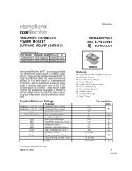
IRF5305S/L - International Rectifier
IRF5305S/L - International Rectifier
IRF5305S/L - International Rectifier

Create successful ePaper yourself
Turn your PDF publications into a flip-book with our unique Google optimized e-Paper software.
l Advanced Process Technology<br />
l Surface Mount (<strong>IRF5305S</strong>)<br />
l Low-profile through-hole (IRF5305L)<br />
l 175°C Operating Temperature<br />
l Fast Switching<br />
l P-Channel<br />
l Fully Avalanche Rated<br />
Description<br />
Fifth Generation HEXFETs from <strong>International</strong> <strong>Rectifier</strong><br />
utilize advanced processing techniques to achieve<br />
extremely low on-resistance per silicon area. This<br />
benefit, combined with the fast switching speed and<br />
ruggedized device design that HEXFET Power MOSFETs<br />
are well known for, provides the designer with an extremely<br />
efficient and reliable device for use in a wide variety of<br />
applications.<br />
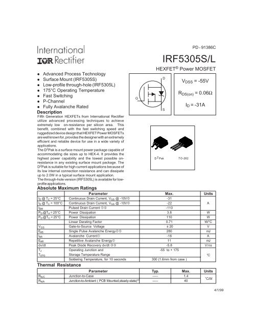
The D 2 Pak is a surface mount power package capable of<br />
accommodating die sizes up to HEX-4. It provides the<br />
highest power capability and the lowest possible onresistance<br />
in any existing surface mount package. The<br />
D 2 Pak is suitable for high current applications because of<br />
its low internal connection resistance and can dissipate<br />
up to 2.0W in a typical surface mount application.<br />
The through-hole version (IRF5305L) is available for lowprofile<br />
applications.<br />
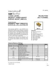
G<br />
PD - 91386C<br />
<strong>IRF5305S</strong>/L<br />
HEXFET ® Power MOSFET<br />
D<br />
S<br />
2 D Pak TO-262<br />
V DSS = -55V<br />
R DS(on) = 0.06Ω<br />
I D = -31A<br />
Absolute Maximum Ratings<br />
Parameter Max. Units<br />
I D @ T C = 25°C Continuous Drain Current, V GS @ -10V… -31<br />
I D @ T C = 100°C Continuous Drain Current, V GS @ -10V… -22 A<br />
I DM Pulsed Drain Current … -110<br />
P D @T A = 25°C Power Dissipation 3.8 W<br />
P D @T C = 25°C Power Dissipation 110 W<br />
Linear Derating Factor 0.71 W/°C<br />
V GS Gate-to-Source Voltage ± 20 V<br />
E AS Single Pulse Avalanche Energy‚… 280 mJ<br />
I AR Avalanche Current -16 A<br />
E AR Repetitive Avalanche Energy 11 mJ<br />
dv/dt Peak Diode Recovery dv/dt ƒ… -5.8 V/ns<br />
T J Operating Junction and -55 to + 175<br />
T STG<br />
Storage Temperature Range<br />
°C<br />
Soldering Temperature, for 10 seconds 300 (1.6mm from case )<br />
Thermal Resistance<br />
Parameter Typ. Max. Units<br />
R θJC Junction-to-Case ––– 1.4<br />
R θJA Junction-to-Ambient ( PCB Mounted,steady-state)** ––– 40<br />
°C/W<br />
4/1/99
<strong>IRF5305S</strong>/L<br />
Electrical Characteristics @ T J = 25°C (unless otherwise specified)<br />
Parameter Min. Typ. Max. Units Conditions<br />
V (BR)DSS Drain-to-Source Breakdown Voltage -55 ––– ––– V V GS = 0V, I D = -250µA<br />
∆V (BR)DSS/∆T J Breakdown Voltage Temp. Coefficient ––– -0.034 ––– V/°C Reference to 25°C, I D = -1mA…<br />
R DS(on) Static Drain-to-Source On-Resistance ––– ––– 0.06 Ω V GS = -10V, I D = -16A „<br />
V GS(th) Gate Threshold Voltage -2.0 ––– -4.0 V V DS = V GS , I D = -250µA<br />
g fs Forward Transconductance 8.0 ––– ––– S V DS = -25V, I D = -16A…<br />
I DSS Drain-to-Source Leakage Current<br />
––– ––– -25 V<br />
µA DS = -55V, V GS = 0V<br />
––– ––– -250 V DS = -44V, V GS = 0V, T J = 150°C<br />
I GSS<br />
Gate-to-Source Forward Leakage ––– ––– 100 V GS = 20V<br />
nA<br />
Gate-to-Source Reverse Leakage ––– ––– -100 V GS = -20V<br />
Q g Total Gate Charge ––– ––– 63 I D = -16A<br />
Q gs Gate-to-Source Charge ––– ––– 13 nC V DS = -44V<br />
Q gd Gate-to-Drain ("Miller") Charge ––– ––– 29 V GS = -10V, See Fig. 6 and 13 „…<br />
t d(on) Turn-On Delay Time ––– 14 ––– V DD = -28V<br />
t r Rise Time ––– 66 ––– I D = -16A<br />
ns<br />
t d(off) Turn-Off Delay Time ––– 39 ––– R G = 6.8Ω<br />
t f Fall Time ––– 63 ––– R D = 1.6Ω, See Fig. 10 „…<br />
L S Internal Source Inductance<br />
––– 7.5 ––– nH<br />
Between lead,<br />
and center of die contact<br />
C iss Input Capacitance ––– 1200 ––– V GS = 0V<br />
C oss Output Capacitance ––– 520 ––– pF V DS = -25V<br />
C rss Reverse Transfer Capacitance ––– 250 ––– ƒ = 1.0MHz, See Fig. 5…<br />
Source-Drain Ratings and Characteristics<br />
Parameter Min. Typ. Max. Units Conditions<br />
D<br />
I S Continuous Source Current MOSFET symbol<br />
––– ––– -31<br />
(Body Diode)<br />
showing the<br />
A<br />
I SM Pulsed Source Current integral reverse<br />
G<br />
––– ––– -110<br />
(Body Diode)<br />
p-n junction diode.<br />
S<br />
V SD Diode Forward Voltage ––– ––– -1.3 V T J = 25°C, I S = -16A, V GS = 0V „<br />
t rr Reverse Recovery Time ––– 71 110 ns T J = 25°C, I F = -16A<br />
Q rr Reverse Recovery Charge ––– 170 250 nC di/dt = -100A/µs „…<br />
t on Forward Turn-On Time Intrinsic turn-on time is negligible (turn-on is dominated by L S +L D )<br />
Notes:<br />
Repetitive rating; pulse width limited by<br />
max. junction temperature. ( See fig. 11 )<br />
„ Pulse width ≤ 300µs; duty cycle ≤ 2%.<br />
‚ V DD = -25V, Starting T J = 25°C, L = 2.1mH … Uses IRF5305 data and test conditions<br />
R G = 25Ω, I AS = -16A. (See Figure 12)<br />
ƒ I SD ≤ -16A, di/dt ≤ -280A/µs, V DD ≤ V (BR)DSS ,<br />
T J ≤ 175°C<br />
** When mounted on 1" square PCB (FR-4 or G-10 Material ).<br />
For recommended footprint and soldering techniques refer to application note #AN-994.<br />
2 www.irf.com
<strong>IRF5305S</strong>/L<br />
-I<br />
D<br />
, Drain-to-Source Current (A)<br />
1000<br />
100<br />
10<br />
VGS<br />
TOP - 15V<br />
- 10V<br />
- 8.0V<br />
- 7.0V<br />
- 6.0V<br />
- 5.5V<br />
- 5.0V<br />
BOTTOM - 4.5V<br />
-4.5V<br />
-I D , Drain-to-Source Current (A)<br />
1000<br />
100<br />
10<br />
VGS<br />
TOP - 15V<br />
- 10V<br />
- 8.0V<br />
- 7.0V<br />
- 6.0V<br />
- 5.5V<br />
- 5.0V<br />
BOTTOM - 4.5V<br />
-4.5V<br />
20µs PULSE WIDTH<br />
20µs PULSE WIDTH<br />
T J c= 25°C T<br />
1<br />
A<br />
1<br />
C J = 175°C<br />
A<br />
0.1 1 10 100<br />
0.1 1 10 100<br />
-V<br />
DS<br />
, Drain-to-Source Voltage (V)<br />
-V DS , Drain-to-Source Voltage (V)<br />
Fig 1. Typical Output Characteristics<br />
Fig 2. Typical Output Characteristics<br />
-I D , Drain-to-Source Current (A)<br />
100<br />
10<br />
T = 25°C<br />
J<br />
T = 175°C<br />
J<br />
V DS= -25V<br />
20µs PULSE W IDTH<br />
1<br />
A<br />
4 5 6 7 8 9 10<br />
-V GS , Gate-to-Source Voltage (V)<br />
Fig 3. Typical Transfer Characteristics<br />
R DS(on) , D rain-to-Source O n R esistance<br />
(Normalized)<br />
2.0<br />
1.5<br />
1.0<br />
0.5<br />
I D = -27A<br />
V GS= -10V<br />
0.0<br />
A<br />
-60 -40 -20 0 20 40 60 80 100 120 140 160 180<br />
T J , Junction Temperature (°C)<br />
Fig 4. Normalized On-Resistance<br />
Vs. Temperature<br />
www.irf.com 3
<strong>IRF5305S</strong>/L<br />
C, Capacitance (pF)<br />
2500<br />
2000<br />
1500<br />
1000<br />
500<br />
V GS = 0V, f = 1MHz<br />
C iss = C gs + C gd , C ds SHORTED<br />
C rss = C gd<br />
C oss = C ds + C gd<br />
C iss<br />
C oss<br />
C rss<br />
-V DS , Drain-to-Source Voltage (V)<br />
-V , Gate-to-Source Voltage (V)<br />
GS<br />
20<br />
16<br />
12<br />
8<br />
4<br />
I D = -16A<br />
V DS = -44V<br />
V DS = -28V<br />
0<br />
A<br />
1 10 100<br />
Fig 5. Typical Capacitance Vs.<br />
Drain-to-Source Voltage<br />
FOR TEST CIRCUIT<br />
0<br />
SEE FIGURE 13<br />
A<br />
0 10 20 30 40 50 60<br />
Q G , Total Gate Charge (nC)<br />
Fig 6. Typical Gate Charge Vs.<br />
Gate-to-Source Voltage<br />
-I SD , Reverse Drain Current (A)<br />
1000<br />
100<br />
T = 175°C<br />
J<br />
T = 25°C<br />
J<br />
V GS = 0V<br />
10<br />
A<br />
0.4 0.8 1.2 1.6 2.0<br />
-V SD , Source-to-Drain Voltage (V)<br />
Fig 7. Typical Source-Drain Diode<br />
Forward Voltage<br />
-I<br />
D<br />
, Drain Current (A)<br />
1000<br />
100<br />
10<br />
OPERATION IN THIS AREA LIMITED<br />
BY R DS(on)<br />
100µs<br />
1ms<br />
T 10ms<br />
C = 25°C<br />
T J = 175°C<br />
Single P u lse<br />
1<br />
A<br />
1 10 100<br />
-V DS , Drain-to-Source Voltage (V)<br />
Fig 8. Maximum Safe Operating Area<br />
4 www.irf.com
<strong>IRF5305S</strong>/L<br />
V DS<br />
R D<br />
35<br />
30<br />
R G<br />
V GS<br />
D.U.T.<br />
-<br />
V DD<br />
-I D , Drain Current (A)<br />
25<br />
20<br />
15<br />
10<br />
5<br />
+<br />
-10V<br />
Pulse Width ≤ 1 µs<br />
Duty Factor ≤ 0.1 %<br />
Fig 10a. Switching Time Test Circuit<br />
t d(on) t r t d(off) t f<br />
V GS<br />
10%<br />
0<br />
25 50 75 100 125 150 175<br />
T C, Case Temperature ( ° C)<br />
90%<br />
V DS<br />
Fig 9. Maximum Drain Current Vs.<br />
Case Temperature<br />
Fig 10b. Switching Time Waveforms<br />
10<br />
Thermal Response (Z thJC )<br />
1<br />
0.1<br />
D = 0.50<br />
0.20<br />
0.10<br />
0.05<br />
0.02<br />
0.01<br />
SINGLE PULSE<br />
(THERMAL RESPONSE)<br />
Notes:<br />
1. Duty factor D = t 1 / t 2<br />
2. Peak T J = P DM x Z thJC + TC<br />
0.01<br />
0.00001 0.0001 0.001 0.01 0.1<br />
t 1, Rectangular Pulse Duration (sec)<br />
PDM<br />
t1<br />
t2<br />
Fig 11. Maximum Effective Transient Thermal Impedance, Junction-to-Case<br />
www.irf.com 5
<strong>IRF5305S</strong>/L<br />
V L<br />
DS<br />
R G<br />
D.U.T<br />
IAS<br />
-20V<br />
tp 0.01Ω<br />
I AS<br />
V DD<br />
A<br />
DRIVER<br />
15V<br />
Fig 12a. Unclamped Inductive Test Circuit<br />
E AS , Single Pulse Avalanche Energy (mJ)<br />
700<br />
600<br />
500<br />
400<br />
300<br />
200<br />
100<br />
ID<br />
TOP -6.6A<br />
-11A<br />
BOTTOM -16A<br />
V DD = -25V<br />
0<br />
A<br />
25 50 75 100 125 150 175<br />
Starting T J , Junction Temperature (°C)<br />
Fig 12c. Maximum Avalanche Energy<br />
Vs. Drain Current<br />
tp<br />
V (BR)DSS<br />
Fig 12b. Unclamped Inductive Waveforms<br />
Current Regulator<br />
Same Type as D.U.T.<br />
-10V<br />
Q G<br />
12V<br />
.2µF<br />
50KΩ<br />
.3µF<br />
Q GS<br />
Q GD<br />
D.U.T.<br />
V + DS<br />
-<br />
V G<br />
V GS<br />
-3mA<br />
Charge<br />
I G I D<br />
Current Sampling Resistors<br />
Fig 13a. Basic Gate Charge Waveform<br />
Fig 13b. Gate Charge Test Circuit<br />
6 www.irf.com
Peak Diode Recovery dv/dt Test Circuit<br />
<strong>IRF5305S</strong>/L<br />
D.U.T*<br />
+<br />
ƒ<br />
-<br />
Circuit Layout Considerations<br />
• Low Stray Inductance<br />
• Ground Plane<br />
• Low Leakage Inductance<br />
Current Transformer<br />
+<br />
‚<br />
-<br />
-<br />
„<br />
+<br />
R G<br />
• dv/dt controlled by R G<br />
• I SD controlled by Duty Factor "D"<br />
• D.U.T. - Device Under Test<br />
+<br />
-<br />
V DD<br />
V GS<br />
[ ]<br />
* Reverse Polarity of D.U.T for P-Channel<br />
Driver Gate Drive<br />
Period<br />
P.W.<br />
D =<br />
P.W.<br />
Period<br />
[ V GS =10V ] ***<br />
D.U.T. I SD Waveform<br />
Reverse<br />
Recovery<br />
Current<br />
Body Diode Forward<br />
Current<br />
di/dt<br />
D.U.T. V DS Waveform<br />
Diode Recovery<br />
dv/dt<br />
V DD<br />
Re-Applied<br />
Voltage<br />
Inductor Curent<br />
Body Diode<br />
Forward Drop<br />
Ripple ≤ 5%<br />
[ ]<br />
I SD<br />
*** V GS = 5.0V for Logic Level and 3V Drive Devices<br />
Fig 14. For P-Channel HEXFETS<br />
www.irf.com 7
<strong>IRF5305S</strong>/L<br />
D 2 Pak Package Outline<br />
1.40 (.055)<br />
M AX.<br />
10.54 (.415)<br />
10.29 (.405)<br />
- A -<br />
2<br />
4.69 (.185)<br />
4.20 (.165)<br />
- B -<br />
1.32 (.052)<br />
1.22 (.048)<br />
10.16 (.400)<br />
REF.<br />
6.47 (.255)<br />
6.18 (.243)<br />
1.78 (.070)<br />
1.27 (.050)<br />
1 3<br />
15.49 (.610)<br />
14.73 (.580)<br />
2.79 (.110)<br />
2.29 (.090)<br />
5.28 (.208)<br />
4.78 (.188)<br />
2.61 (.103)<br />
2.32 (.091)<br />
3X<br />
1.40 (.055)<br />
1.14 (.045)<br />
5.08 (.200)<br />
3X<br />
0.93 (.037)<br />
0.69 (.027)<br />
0.55 (.022)<br />
0.46 (.018)<br />
1.39 (.055)<br />
1.14 (.045)<br />
8.89 (.350)<br />
REF.<br />
0.25 (.010) M B A M MINIMUM RECOMMENDED FOOTPRINT<br />
11.43 (.450)<br />
NOTES:<br />
1 DIMENSIONS AFTER SOLDER DIP.<br />
2 DIMENSIONING & TOLERANCING PER ANSI Y14.5M, 1982.<br />
3 CONTROLLING DIMENSION : INCH.<br />
4 HEATSINK & LEAD DIMENSIONS DO NOT INCLUDE BURRS.<br />
LEAD ASSIGNMENTS<br />
1 - GATE<br />
2 - DRAIN<br />
3 - SOURCE<br />
8.89 (.350)<br />
3.81 (.150)<br />
17.78 (.700)<br />
2.08 (.082)<br />
2X<br />
2.54 (.100)<br />
2X<br />
Part Marking Information<br />
D 2 Pak<br />
INTERNATIONAL<br />
RECTIFIER<br />
LOGO<br />
ASSEMBLY<br />
LOT CODE<br />
F530S<br />
9246<br />
9B 1M<br />
PART NUMBER<br />
DATE CODE<br />
(YYW W )<br />
YY = YEAR<br />
WW = WEEK<br />
A<br />
8 www.irf.com
<strong>IRF5305S</strong>/L<br />
Package Outline<br />
TO-262 Outline<br />
Part Marking Information<br />
TO-262<br />
www.irf.com 9
<strong>IRF5305S</strong>/L<br />
Tape & Reel Information<br />
D 2 Pak<br />
TRR<br />
1.60 (.063)<br />
1.50 (.059)<br />
4.10 (.161)<br />
3.90 (.153)<br />
1.60 (.063)<br />
1.50 (.059)<br />
0.368 (.0145)<br />
0.342 (.0135)<br />
FEED DIRECTION<br />
1.85 (.073)<br />
1.65 (.065)<br />
11.60 (.457)<br />
11.40 (.449)<br />
15.42 (.609)<br />
15.22 (.601)<br />
24.30 (.957)<br />
23.90 (.941)<br />
TRL<br />
10.90 (.429)<br />
10.70 (.421)<br />
16.10 (.634)<br />
15.90 (.626)<br />
1.75 (.069)<br />
1.25 (.049)<br />
4.72 (.136)<br />
4.52 (.178)<br />
FEED DIRECTION<br />
13.50 (.532)<br />
12.80 (.504)<br />
27.40 (1.079)<br />
23.90 (.941)<br />
4<br />
330.00<br />
(14.173)<br />
MAX.<br />
60.00 (2.362)<br />
MIN.<br />
NOTES :<br />
1. COMFORMS TO EIA-418.<br />
2. CONTROLLING DIMENSION: MILLIMETER.<br />
3. DIMENSION MEASURED @ HUB.<br />
4. INCLUDES FLANGE DISTORTION @ OUTER EDGE.<br />
26.40 (1.039)<br />
24.40 (.961)<br />
3<br />
30.40 (1.197)<br />
MAX.<br />
4<br />
WORLD HEADQUARTERS: 233 Kansas St., El Segundo, California 90245, Tel: (310) 322 3331<br />
IR GREAT BRITAIN: Hurst Green, Oxted, Surrey RH8 9BB, UK Tel: ++ 44 1883 732020<br />
IR CANADA: 15 Lincoln Court, Brampton, Ontario L6T3Z2, Tel: (905) 453 2200<br />
IR GERMANY: Saalburgstrasse 157, 61350 Bad Homburg Tel: ++ 49 6172 96590<br />
IR ITALY: Via Liguria 49, 10071 Borgaro, Torino Tel: ++ 39 11 451 0111<br />
IR FAR EAST: K&H Bldg., 2F, 30-4 Nishi-Ikebukuro 3-Chome, Toshima-Ku, Tokyo Japan 171 Tel: 81 3 3983 0086<br />
IR SOUTHEAST ASIA: 1 Kim Seng Promenade, Great World City West Tower, 13-11, Singapore 237994 Tel: ++ 65 838 4630<br />
IR TAIWAN:16 Fl. Suite D. 207, Sec. 2, Tun Haw South Road, Taipei, 10673, Taiwan Tel: 886-2-2377-9936<br />
http://www.irf.com/ Data and specifications subject to change without notice. 4/99<br />
10 www.irf.com
Note: For the most current drawings please refer to the IR website at:<br />
http://www.irf.com/package/