IR1150(S)(PbF) IR1150I(S)(PbF)
IR1150(S)(PbF) IR1150I(S)(PbF)
IR1150(S)(PbF) IR1150I(S)(PbF)

Create successful ePaper yourself
Turn your PDF publications into a flip-book with our unique Google optimized e-Paper software.
<strong>IR1150</strong>(S)/<strong>IR1150</strong>I(S)(<strong>PbF</strong>)Electrical Characteristics cont.The electrical characteristics involve the spread of values guaranteed within the specified supply voltage and junctiontemperature range T J from – 25°C to 125°C. Typical values represent the median values, which are related to 25°C. If nototherwise stated, a supply voltage of V CC =15V is assumed for test condition.Parameters Symbols Min. Typ. Max. Units RemarksVCC turn-off hysteresis V CC HYST 1.8 — 2.2 V— 18 22 mA C LOAD =1nF f SW =200kHZ— 36 40 mA C LOAD =10nF f SW =200kHZOperating currentI CCStandby mode - inactive gate— 8 10 mAInternal oscillator runningStartup current I CCSTART — — 175 uA V CC =V CC ON - 0.1VSleep current I SLEEP — 125 200 uA V OVP
<strong>IR1150</strong>(S)/<strong>IR1150</strong>I(S)(<strong>PbF</strong>)Internal Voltage Reference SectionParameters Symbols Min. Typ. Max. Units RemarksReference voltage V REF 6.9 7.0 7.1 V T A = 25˚CLine regulation R REG — 12 25 mV 13.5V
<strong>IR1150</strong>(S)/<strong>IR1150</strong>I(S)(<strong>PbF</strong>)Gate Driver SectionParameters Symbols Min. Typ. Max. Units RemarksGate low voltage V GLO — 1.2 1.5 V I GATE =200mAGate high voltage V GTH — 13 18 V V CC =20VGate high voltage V GTH 9.5 — — V V CC =11.5VRise timeFall timetrtf— 20 — ns C LOAD = 1nF, V CC =16V— 70 — ns C LOAD = 10nF, V CC =16V— 20 — ns C LOAD = 1nF, V CC =16V— 70 — ns C LOAD = 10nF, V CC =16VOut peak current I OPK 1.5 — — A C LOAD = 10nF, V CC =16VGate voltage @ fault VG fault — — 1.8 V I GATE =20mANote 1: Guaranteed by design, but not tested in production.www.irf.com 5
Block Diagram<strong>IR1150</strong>(S)/<strong>IR1150</strong>I(S)(<strong>PbF</strong>)0.62VLead Assignments & DefinitionsLead Assignment Pin# Symbol Description1 COM Ground2 FREQ Frequency Set3 I SNS Current Sense4 OVP/EN Overvoltage Fault Detect / Enable5 COMP Voltage Loop Compensation6 V FB Output Voltage Sense7 V CC IC Supply Voltage8 GATE Gate Drive Outputwww.irf.com 6
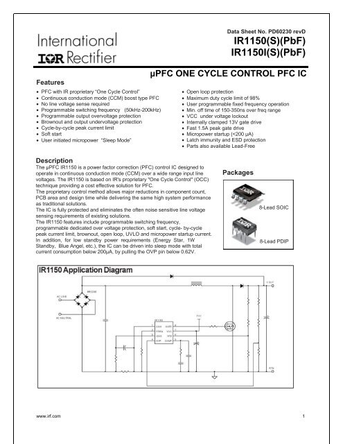
<strong>IR1150</strong>(S)/<strong>IR1150</strong>I(S)(<strong>PbF</strong>)General DescriptionThe µPFC <strong>IR1150</strong> is intended for boost converters forpower factor correction operating at a fixed frequency incontinuous conduction mode. The IC operates with twoloops; an inner current loop and an outer voltage loop.The inner current loop is fast, reliable and does notrequire sensing of the input voltage in order to create acurrent reference.This inner current loop sustains the sinusoidal profile ofthe average input current based on the dependency ofthe pulse width modulator duty cycle on the input linevoltage in order to determine the analogous input linecurrent. Thus, the current loop uses the embeddedinput voltage signal to control the average input currentto follow the input voltage.The <strong>IR1150</strong> enables excellent THD performance. Inlight load conditions, a small distortion occurs at zerocrossingdue to the finite boost inductance but this isnegligible and well within EN61000-3-2 Class Dspecifications.The outer voltage loop controls the DC bus voltage.This voltage is fed into the voltage error amplifier tocontrol the slope of the integrator ramp and sets theamplitude of the average input current.The two loops combine to control the amplitude, phaseand shape of the input current, with respect to the inputvoltage, giving near-unity power factor.The IC is designed for robust operation and providesprotection from system level over current, over voltage,under voltage, and brownout conditions.IC SupplyThe UVLO circuit monitors the VCC pin and maintains thegate drive signal inactive until the VCC pin voltagereaches the UVLO turn on threshold, (V CC ON ). As soon asthe VCC voltage exceeds this threshold, provided that theV FB pin voltage is greater than 20%VREF, the gate drivewill begin switching (under Soft Start) and increase thepulse width to its maximum value as demanded by theoutput voltage error amplifier. If the voltage on the VCCpin falls below the UVLO turn off threshold, (V CC UVLO ), theIC turns off, gate drive is terminated, and the turn onthreshold must again be exceeded in order to re-start theprocess and move into Soft Start mode.Soft StartSoft Start controls the rate of rise of the output voltageerror amplifier in order to obtain a linear control of theincreasing duty cycle as a function of time. The Soft Starttime is controlled by voltage error amplifier compensationcomponents selected, and is user programmable basedon desired loop crossover frequency.Frequency SelectThe switching frequency of the IC is programmable by anexternal resistor at the FREQ pin. The designincorporates min/max restrictions such that the minimumand maximum operating frequency fall within the range of50-200kHz.Gate DriveThe gate drive is a totem pole driver with 1.5A capability.If higher currents are required, additional external driverscan be used.www.irf.com 7
<strong>IR1150</strong>(S)/<strong>IR1150</strong>I(S)(<strong>PbF</strong>)Detailed Pin DescriptionCOM: GroundThis is the ground potential pin of the integrated controlcircuit. All internal devices are referenced to this point.V FB : Output Voltage FeedbackThe output voltage of the boost converter is sensed via aresistive divider and fed into this pin, which is the invertinginput of the output voltage error amplifier. The impedanceof the divider string must be low enough so as to notintroduce substantial error due to the input bias currents ofthe amplifier, yet high enough so as to minimize powerdissipation. A typical value of external divider impedanceis 1MΩ.The error amplifier is a transconductance type which yieldshigh output impedance, thus increasing the noise immunityof the error amplifier output. This also eliminates inputdivider string interaction with compensation feedbackcapacitors and reducing the loading of divider string due toa low impedance output of the amplifier.COMP: Voltage Loop CompensationExternal circuitry from this pin to ground compensates thesystem voltage loop and soft start time. This is the outputof the voltage error amplifier. This pin will be dischargedvia internal resistance when a fault mode occurs.GATE: Gate Drive OutputThis is the gate drive output of the IC. Drive voltage isinternally limited and provides ±1.5A peak with matchedrise and fall times.FREQ: Frequency SetThis is the user programmable frequency pin. Anexternal resistor from this pin to the COM pin programsthe frequency. The operational switchingfrequency range for the device is 50kHz – 200kHz.ISNS: Current Sense inputThis pin is the inverting Current Sense Input & PeakCurrent Limit. The voltage at this pin is the negativevoltage drop, sensed across the system current senseresistor, representing the inductor current.This voltage is fed into the Peak Current Limit protectioncomparator with threshold around -1V. This protectioncircuit incorporates a leading edge blanking circuitfollowing the comparator to improve noise immunity of theprotection process.The current sense signal is also fed into the current senseamplifier. The signal is amplified, filtered of high frequencynoise and then injected into a summing node where it issubtracted from the compensation voltage V COMP .The signal on this pin must be previously filtered with anRC cell to provide additional noise immunity. The inputimpedance of this pin is 5kΩ .V CC : Supply VoltageThis is the supply voltage pin of the IC and it is monitoredby the under voltage lockout circuit. It is possible to turnoff the IC by pulling this pin below the minimum turn offthreshold voltage, without damage to the IC.To prevent noise problems, a bypass ceramic capacitorconnected to VCC and COM should be placed as close aspossible to the <strong>IR1150</strong>.This pin is not internally clamped, therefore damage willoccur if the maximum voltage is exceeded.OVP/EN: Over Voltage Protection / EnableThis pin is the input to the over voltage protectioncomparator the threshold of which is internallyprogrammed to 105.5% of VREF.A resistive divider feeds this pin from the output volt-ageto COM and inhibits the gate drive whenever the thresholdis exceeded. Normal operation resumes when the voltagelevel on this pin decreases to below the pin threshold.This pin is also used to activate “sleep” mode by pullingthe voltage level below 0.62V (typ).www.irf.com 8
<strong>IR1150</strong>(S)/<strong>IR1150</strong>I(S)(<strong>PbF</strong>)Operating StatesUVLO ModeThe IC remains in the UVLO condition until the voltage onthe V CC pin exceeds the VCC turn on threshold voltage,VCC ON.During the time the IC remains in the UVLO state, the gatedrive circuit is inactive and the IC draws aquiescent current of ICC START. The UVLO mode isaccessible from any other state of operation whenever theIC supply voltage condition of V CC < V CC UVLO occurs.Standby ModeThe IC is in this state if the supply voltage has exceededV CC ON and the VFB pin voltage is less than 20% of VREF .The oscillator is running and all internal circuitry is biasedin this state but the gate is inactive. This state isaccessible from any other state of operation except OVP.The IC enters this state whenever the VFB pin voltage hasdecreased to 50% of VREF when operating in normalmode or during a peak current limit fault condition, or 20%VREF when operating in soft start mode.Soft Start ModeThis state is activated once the V CC voltage hasexceeded V CCON and the VFB pin voltage has exceeded20% of VREF.The soft start time, which is defined as the time requiredfor the duty cycle to linearly increase from zero tomaximum, is dependent upon the values selected forcompensation of the voltage loop pin COMP to pin COM.Throughout the soft start cycle, the output of the voltageerror amplifier (pin COMP) charges through thecompensation network. This forces a linear rise of thevoltage at this node which in turn forces a linear increasein the gate drive duty cycle from 0. This controlled dutycycle reduces system component stress during start upconditions as the input current amplitude is increasinglinearly.Normal ModeThe IC enters normal operating mode once the soft starttransition has been completed. At this point the gate driveis switching and the IC draws a maximum of ICC from thesupply voltage source. The device will initiate another softstart sequence in the event of a shutdown due to a fault,which activates the protection circuitry, or if the supplyvoltage drops below the UVLO turn off threshold of V CCUVLO.Fault Protection ModeThe fault mode will be activated when any of the protectioncircuits are activated. The IC protection circuits includeSupply Voltage Under Voltage Lockout (UVLO), OutputOver Voltage Protection (OVP), Open Loop Protection(OLP), Output Undervoltage Protection (OUV), and PeakCurrent Limit Protection (I PK LIMIT ).Sleep ModeThe sleep mode is initiated by pulling the OVP pin below0.62V (typ). In this mode the IC draws a very lowquiescent supply current.www.irf.com 9
<strong>IR1150</strong>(S)/<strong>IR1150</strong>I(S)(<strong>PbF</strong>)V OVP 0.62VV OVP
<strong>IR1150</strong>(S)/<strong>IR1150</strong>I(S)(<strong>PbF</strong>)www.irf.com 11
<strong>IR1150</strong>(S)/<strong>IR1150</strong>I(S)(<strong>PbF</strong>)www.irf.com 12
<strong>IR1150</strong>(S)/<strong>IR1150</strong>I(S)(<strong>PbF</strong>)www.irf.com 13
<strong>IR1150</strong>(S)/<strong>IR1150</strong>I(S)(<strong>PbF</strong>)www.irf.com 14
<strong>IR1150</strong>(S)/<strong>IR1150</strong>I(S)(<strong>PbF</strong>)Tape & Reel Information (SOIC 8-Lead only)Dimensions are shown in millimeters (inches)TERMINAL NUMBER 112.3 ( .484 )11.7 ( .461 )8.1 ( .318 )7.9 ( .312 )FEED DIRECTIONNOTES:1. OUTLINE CONFORMS TO EIA-481 & EIA-541.2. CONTROLLING DIMENSION : MILLIMETER.330.00(12.992) MAX.NOTES :1. CONTROLLING DIMENSION : MILLIMETER.2. OUTLINE CONFORMS TO EIA-481 & EIA-541.14.40 ( .566 )12.40 ( .488 )www.irf.com 15
<strong>IR1150</strong>(S)/<strong>IR1150</strong>I(S)(<strong>PbF</strong>)PART MARKING INFORMATIONORDER INFORMATIONBasic PartLead-free Part8-Lead SOIC <strong>IR1150</strong>STR order <strong>IR1150</strong>STR 8-Lead SOIC <strong>IR1150</strong>S order <strong>IR1150</strong>STR<strong>PbF</strong>8-Lead SOIC <strong>IR1150</strong>ISTR order <strong>IR1150</strong>ISTR 8-Lead SOIC <strong>IR1150</strong>ISTR order <strong>IR1150</strong>ISTR<strong>PbF</strong>8-Lead PDIP <strong>IR1150</strong> order <strong>IR1150</strong><strong>PbF</strong>8-Lead PDIP <strong>IR1150</strong>I order <strong>IR1150</strong>I<strong>PbF</strong>The <strong>IR1150</strong>(S)(<strong>PbF</strong>) has been designed and qualified for the Consumer MarketThe <strong>IR1150</strong>I(S)(<strong>PbF</strong>) has been designed and qualified for the Industrial MarketQualification Standards can be found on IR’s Web site.WORLD HEADQUARTERS: 233 Kansas Street, El Segundo, California 90245 Tel: (310) 252-7105http://www.irf.com/ Data and specifications subject to change without notice. 2/5/2007www.irf.com 16