IRF8313PBF Datasheet - International Rectifier
IRF8313PBF Datasheet - International Rectifier
IRF8313PBF Datasheet - International Rectifier

Create successful ePaper yourself
Turn your PDF publications into a flip-book with our unique Google optimized e-Paper software.
Applications<br />
l Load Switch<br />
l DC/DC Conversion<br />
Benefits<br />
l Low Gate Charge and Low R DS(on)<br />
l Fully Characterized Avalanche Voltage<br />
and Current<br />
l 20V V GS Max. Gate Rating<br />
l 100% Tested for R G<br />
l Lead-Free (Qualified to 260°C Reflow)<br />
l RoHS Compliant (Halogen Free)<br />
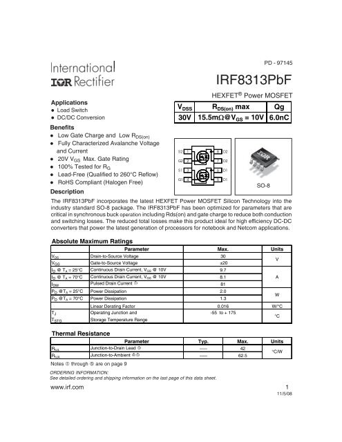
Description<br />
IRF8313PbF<br />
HEXFET ® Power MOSFET<br />
SO-8<br />
PD - 97145<br />
V DSS R DS(on) max Qg<br />
30V 15.5m:@V GS = 10V 6.0nC<br />
The IRF8313PbF incorporates the latest HEXFET Power MOSFET Silicon Technology into the<br />
industry standard SO-8 package. The IRF8313PbF has been optimized for parameters that are<br />
critical in synchronous buck operation including Rds(on) and gate charge to reduce both conduction<br />
and switching losses. The reduced total losses make this product ideal for high efficiency DC-DC<br />
converters that power the latest generation of processors for notebook and Netcom applications.<br />
S2 1<br />
G2 2<br />
S1<br />
3<br />
G1 4<br />
8<br />
7<br />
6<br />
5<br />
D2<br />
D2<br />
D1<br />
D1<br />
Absolute Maximum Ratings<br />
Parameter<br />
V DS<br />
V GS<br />
I D @ T A = 25°C<br />
I D @ T A = 70°C<br />
I DM<br />
P D @T A = 25°C<br />
P D @T A = 70°C<br />
T J<br />
T STG<br />
Drain-to-Source Voltage<br />
Gate-to-Source Voltage<br />
Continuous Drain Current, V GS @ 10V<br />
Continuous Drain Current, V GS @ 10V<br />
Pulsed Drain Current c<br />
Power Dissipation<br />
Power Dissipation<br />
Linear Derating Factor<br />
Operating Junction and<br />
Storage Temperature Range<br />
Max.<br />
30<br />
±20<br />
9.7<br />
8.1<br />
81<br />
2.0<br />
1.3<br />
0.016<br />
-55 to + 175<br />
Units<br />
V<br />
A<br />
W<br />
W/°C<br />
°C<br />
Thermal Resistance<br />
Parameter Typ. Max. Units<br />
R θJL<br />
Junction-to-Drain Lead g ––– 42<br />
°C/W<br />
R θJA<br />
Junction-to-Ambient fg ––– 62.5<br />
Notes through … are on page 9<br />
ORDERING INFORMATION:<br />
See detailed ordering and shipping information on the last page of this data sheet.<br />
www.irf.com 1<br />
11/5/08
IRF8313PbF<br />
Static @ T J = 25°C (unless otherwise specified)<br />
Parameter Min. Typ. Max. Units<br />
BV DSS Drain-to-Source Breakdown Voltage 30 ––– ––– V V GS = 0V, I D = 250μA<br />
ΔΒV DSS /ΔT J Breakdown Voltage Temp. Coefficient ––– 0.021 ––– V/°C Reference to 25°C, I D = 1mA<br />
R DS(on) Static Drain-to-Source On-Resistance ––– 12.5 15.5 V GS = 10V, I D = 9.7A e<br />
mΩ<br />
––– 18.6 21.6 V GS = 4.5V, I D = 8.0A e<br />
V GS(th) Gate Threshold Voltage 1.35 1.80 2.35 V V DS = V GS , I D = 25μA<br />
ΔV GS(th) Gate Threshold Voltage Coefficient ––– -6.0 ––– mV/°C<br />
I DSS Drain-to-Source Leakage Current ––– ––– 1.0 V<br />
μA DS = 24V, V GS = 0V<br />
––– ––– 150 V DS = 24V, V GS = 0V, T J = 125°C<br />
I GSS Gate-to-Source Forward Leakage ––– ––– 100 V<br />
nA GS = 20V<br />
Gate-to-Source Reverse Leakage ––– ––– -100 V GS = -20V<br />
gfs Forward Transconductance 23 ––– ––– S V DS = 15V, I D = 8.0A<br />
Q g Total Gate Charge ––– 6.0 9.0<br />
Q gs1 Pre-Vth Gate-to-Source Charge ––– 1.5 ––– V DS = 15V<br />
Q gs2 Post-Vth Gate-to-Source Charge ––– 0.9 ––– V<br />
nC GS = 4.5V<br />
Q gd Gate-to-Drain Charge ––– 2.2 ––– I D = 8.0A<br />
Q godr Gate Charge Overdrive ––– 1.4 ––– See Figs. 17a & 17b<br />
Q sw Switch Charge (Q gs2 + Q gd ) ––– 2.9 –––<br />
Q oss Output Charge ––– 3.8 ––– nC V DS = 16V, V GS = 0V<br />
R g Gate Resistance ––– 2.2 3.6 Ω<br />
t d(on) Turn-On Delay Time ––– 8.3 ––– V DD = 15V, V GS = 4.5V<br />
t r Rise Time ––– 9.9 ––– I<br />
ns D = 8.0A<br />
t d(off) Turn-Off Delay Time ––– 8.5 ––– R G = 1.8Ω<br />
t f Fall Time ––– 4.2 ––– See Fig. 15a & 15b<br />
C iss Input Capacitance ––– 760 ––– V GS = 0V<br />
C oss Output Capacitance ––– 172 ––– pF V DS = 15V<br />
C rss Reverse Transfer Capacitance ––– 87 ––– ƒ = 1.0MHz<br />
Avalanche Characteristics<br />
Parameter<br />
Typ.<br />
Max.<br />
Units<br />
E AS<br />
Single Pulse Avalanche Energy d –––<br />
46<br />
mJ<br />
I AR<br />
Avalanche Current c –––<br />
8.0<br />
A<br />
Diode Characteristics<br />
Parameter Min. Typ. Max. Units<br />
Conditions<br />
Conditions<br />
D<br />
I S Continuous Source Current ––– –––<br />
MOSFET symbol<br />
3.1 A<br />
(Body Diode)<br />
showing the<br />
G<br />
I SM Pulsed Source Current ––– –––<br />
integral reverse<br />
82 A<br />
S<br />
(Body Diode)c<br />
p-n junction diode.<br />
V SD Diode Forward Voltage ––– ––– 1.0 V T J = 25°C, I S = 8.0A, V GS = 0V e<br />
t rr Reverse Recovery Time ––– 20 30 ns T J = 25°C, I F = 8.0A, V DD = 15V<br />
Q rr Reverse Recovery Charge ––– 10 15 nC di/dt = 100A/μs e<br />
t on Forward Turn-On Time Intrinsic turn-on time is negligible (turn-on is dominated by LS+LD)<br />
2 www.irf.com
I D , Drain-to-Source Current (A)<br />
I D , Drain-to-Source Current (A)<br />
R DS(on) , Drain-to-Source On Resistance<br />
I D , Drain-to-Source Current (A)<br />
(Normalized)<br />
IRF8313PbF<br />
100<br />
10<br />
VGS<br />
TOP 10V<br />
5.0V<br />
4.5V<br />
3.5V<br />
3.0V<br />
2.7V<br />
2.5V<br />
BOTTOM 2.3V<br />
100<br />
10<br />
VGS<br />
TOP 10V<br />
5.0V<br />
4.5V<br />
3.5V<br />
3.0V<br />
2.7V<br />
2.5V<br />
BOTTOM 2.3V<br />
1<br />
0.1<br />
≤60μs PULSE WIDTH<br />
Tj = 25°C<br />
2.3V<br />
0.01<br />
0.1 1 10 100<br />
V DS , Drain-to-Source Voltage (V)<br />
1<br />
2.3V<br />
≤60μs PULSE WIDTH<br />
Tj = 175°C<br />
0.1<br />
0.1 1 10 100<br />
V DS , Drain-to-Source Voltage (V)<br />
Fig 1. Typical Output Characteristics<br />
Fig 2. Typical Output Characteristics<br />
100<br />
2.0<br />
I D = 9.8A<br />
V GS = 10V<br />
10<br />
T J = 175°C<br />
1.5<br />
1<br />
T J = 25°C<br />
1.0<br />
0.1<br />
0.01<br />
V DS = 15V<br />
≤60μs PULSE WIDTH<br />
1 2 3 4 5 6<br />
V GS , Gate-to-Source Voltage (V)<br />
0.5<br />
-60 -40 -20 0 20 40 60 80 100 120 140 160 180<br />
T J , Junction Temperature (°C)<br />
Fig 3. Typical Transfer Characteristics<br />
Fig 4. Normalized On-Resistance<br />
vs. Temperature<br />
www.irf.com 3
C, Capacitance (pF)<br />
I SD , Reverse Drain Current (A)<br />
I D , Drain-to-Source Current (A)<br />
V GS , Gate-to-Source Voltage (V)<br />
IRF8313PbF<br />
10000<br />
V GS = 0V, f = 1 MHZ<br />
C iss<br />
= C gs<br />
+ C gd<br />
, C ds<br />
SHORTED<br />
C rss<br />
= C gd<br />
C oss<br />
= C ds<br />
+ C gd<br />
16<br />
12<br />
I D = 8.0A<br />
V DS = 24V<br />
V DS = 15V<br />
1000<br />
Ciss<br />
Coss<br />
8<br />
100<br />
Crss<br />
4<br />
10<br />
0.1 1 10 100<br />
V DS , Drain-to-Source Voltage (V)<br />
0<br />
0 2 4 6 8 10 12 14<br />
Q g , Total Gate Charge (nC)<br />
Fig 5. Typical Capacitance vs.<br />
Drain-to-Source Voltage<br />
Fig 6. Typical Gate Charge vs.<br />
Gate-to-Source Voltage<br />
100<br />
1000<br />
OPERATION IN THIS AREA<br />
LIMITED BY R DS (on)<br />
T J = 175°C<br />
100<br />
10<br />
100μsec<br />
T J = 25°C<br />
1<br />
V GS = 0V<br />
0.1<br />
0.2 0.4 0.6 0.8 1.0 1.2 1.4 1.6 1.8<br />
V SD , Source-to-Drain Voltage (V)<br />
10<br />
1<br />
0.1<br />
T A = 25°C<br />
Tj = 175°C<br />
Single Pulse<br />
1msec<br />
10msec<br />
0 1 10 100<br />
V DS , Drain-to-Source Voltage (V)<br />
Fig 7. Typical Source-Drain Diode<br />
Forward Voltage<br />
Fig 8. Maximum Safe Operating Area<br />
4 www.irf.com
I D , Drain Current (A)<br />
V GS(th) , Gate Threshold Voltage (V)<br />
IRF8313PbF<br />
10<br />
2.5<br />
8<br />
2.0<br />
I D = 250μA<br />
6<br />
I D = 25μA<br />
1.5<br />
4<br />
2<br />
1.0<br />
0<br />
25 50 75 100 125 150 175<br />
T A , Ambient Temperature (°C)<br />
0.5<br />
-75 -50 -25 0 25 50 75 100 125 150 175<br />
T J , Temperature ( °C )<br />
Fig 9. Maximum Drain Current vs.<br />
Ambient Temperature<br />
Fig 10. Threshold Voltage vs. Temperature<br />
100<br />
D = 0.50<br />
Thermal Response ( Z thJA )<br />
10<br />
1<br />
0.1<br />
0.01<br />
0.20<br />
0.10<br />
0.05<br />
0.02<br />
0.01<br />
τJ<br />
τJ<br />
τ1<br />
τ1<br />
R1<br />
R1<br />
Ci= τi/Ri<br />
Ci i/Ri<br />
SINGLE PULSE<br />
( THERMAL RESPONSE ) Notes:<br />
1. Duty Factor D = t1/t2<br />
2. Peak Tj = P dm x Zthja + Tc<br />
1E-006 1E-005 0.0001 0.001 0.01 0.1 1 10 100 1000<br />
τ2<br />
τ2<br />
R2<br />
R2<br />
R3<br />
R3<br />
t 1 , Rectangular Pulse Duration (sec)<br />
τ3<br />
τ3<br />
R4<br />
R4<br />
τ4<br />
τ4<br />
R5<br />
R5<br />
τ5<br />
τ5<br />
R6<br />
R6<br />
τ6<br />
τ6<br />
R7<br />
R7<br />
τ7<br />
τ7<br />
R8<br />
R8<br />
τ8<br />
τ8<br />
τa<br />
Ri (°C/W) τι (sec)<br />
0.1396039 0.000010<br />
0.4048955 0.000030<br />
0.5273926 0.000020<br />
1.2084906 0.001289<br />
1.5779475 0.000340<br />
7.0394610 0.009747<br />
18.0102679 27.798341<br />
33.5929564 0.575346<br />
Fig 11. Maximum Effective Transient Thermal Impedance, Junction-to-Ambient<br />
www.irf.com 5
R DS (on), Drain-to -Source On Resistance (mΩ)<br />
E AS, Single Pulse Avalanche Energy (mJ)<br />
IRF8313PbF<br />
38<br />
34<br />
30<br />
I D = 9.8A<br />
200<br />
160<br />
I D<br />
TOP 3.0A<br />
5.0A<br />
BOTTOM 8.0A<br />
26<br />
120<br />
22<br />
18<br />
14<br />
T J = 125°C<br />
T J = 25°C<br />
80<br />
40<br />
10<br />
2.0 4.0 6.0 8.0 10.0<br />
V GS , Gate-to-Source Voltage (V)<br />
0<br />
25 50 75 100 125 150 175<br />
Starting T J , Junction Temperature (°C)<br />
Fig 12. On-Resistance vs. Gate Voltage<br />
Fig 13. Maximum Avalanche Energy<br />
vs. Drain Current<br />
15V<br />
tp<br />
V (BR)DSS<br />
V DS<br />
+<br />
L<br />
DRIVER<br />
R G<br />
20V V GS<br />
Fig 14a. Unclamped Inductive Test Circuit<br />
R G<br />
tp<br />
D.U.T<br />
I AS<br />
0.01Ω<br />
Fig 14b. Unclamped Inductive Waveforms<br />
V DS<br />
R D<br />
V DS<br />
90%<br />
V GS<br />
D.U.T.<br />
Pulse Width ≤ 1 µs<br />
Duty Factor ≤ 0.1 %<br />
- V DD<br />
A<br />
I AS<br />
10%<br />
V GS<br />
t d(on) t r t d(off) t f<br />
Fig 15a. Switching Time Test Circuit<br />
Fig 15b. Switching Time Waveforms<br />
6 www.irf.com
IRF8313PbF<br />
+<br />
‚<br />
-<br />
D.U.T<br />
+<br />
ƒ<br />
-<br />
Circuit Layout Considerations<br />
• Low Stray Inductance<br />
• Ground Plane<br />
• Low Leakage Inductance<br />
Current Transformer<br />
-<br />
„<br />
+<br />
Reverse<br />
Recovery<br />
Current<br />
Driver Gate Drive<br />
Period<br />
P.W.<br />
D.U.T. I SD Waveform<br />
Body Diode Forward<br />
Current<br />
di/dt<br />
D.U.T. V DS Waveform<br />
Diode Recovery<br />
dv/dt<br />
D =<br />
P.W.<br />
Period<br />
V GS =10V<br />
V DD<br />
*<br />
R G<br />
• dv/dt controlled by RG<br />
• Driver same type as D.U.T.<br />
• I SD controlled by Duty Factor "D"<br />
• D.U.T. - Device Under Test<br />
V DD<br />
+<br />
-<br />
Re-Applied<br />
Voltage<br />
Inductor Curent<br />
Body Diode<br />
Forward Drop<br />
Ripple ≤ 5%<br />
I SD<br />
* V GS = 5V for Logic Level Devices<br />
Fig 16. Peak Diode Recovery dv/dt Test Circuit for N-Channel<br />
HEXFET ® Power MOSFETs<br />
Id<br />
Vds<br />
Vgs<br />
0<br />
20K 1K<br />
S<br />
DUT<br />
L<br />
VCC<br />
Vgs(th)<br />
Qgodr<br />
Qgd<br />
Qgs2<br />
Qgs1<br />
Fig 17a. Gate Charge Test Circuit<br />
Fig 17b. Gate Charge Waveform<br />
www.irf.com 7
IRF8313PbF<br />
SO-8 Package Outline<br />
Dimensions are shown in milimeters (inches)<br />
A<br />
E<br />
6<br />
6X<br />
D<br />
5<br />
8 7 6 5<br />
1 2 3 4<br />
e<br />
B<br />
H<br />
0.25 [.010] A<br />
DIM<br />
INCHES MILLIME T E RS<br />
MIN MAX MIN MAX<br />
A<br />
A1<br />
.0532<br />
.0040<br />
.0688<br />
.0098<br />
1.35<br />
0.10<br />
1.75<br />
0.25<br />
b .013 .020 0.33 0.51<br />
c .0075 .0098 0.19 0.25<br />
D<br />
E<br />
e<br />
e1<br />
H<br />
K<br />
L<br />
y<br />
.189 .1968<br />
.1497 .1574<br />
.050 BAS IC 1.27 BAS IC<br />
.025 BAS IC 0.635 BASIC<br />
.2284 .2440<br />
.0099 .0196<br />
.016 .050<br />
0° 8°<br />
4.80 5.00<br />
3.80 4.00<br />
5.80 6.20<br />
0.25 0.50<br />
0.40 1.27<br />
0° 8°<br />
e1<br />
A<br />
C<br />
y<br />
K x 45°<br />
8X b<br />
A1<br />
0.25 [.010] C A B<br />
0.10 [.004]<br />
8X L<br />
7<br />
8X c<br />
F OOT PRINT<br />
NOTES :<br />
1. DIMENS IONING & TOLERANCING PER AS ME Y14.5M-1994.<br />
2. CONTROLLING DIMENSION: MILLIMETER<br />
3. DIMENS IONS ARE SHOWN IN MILLIMETERS [INCHES ].<br />
4. OUTLINE CONFORMS TO JEDEC OUTLINE MS-012AA.<br />
5 DIMENS ION DOES NOT INCLUDE MOLD PROT RUSIONS .<br />
MOLD PROTRUSIONS NOT T O EXCEED 0.15 [.006].<br />
6 DIMENS ION DOES NOT INCLUDE MOLD PROT RUSIONS .<br />
MOLD PROTRUSIONS NOT T O EXCEED 0.25 [.010].<br />
7 DIMENS ION IS THE LENGTH OF LEAD FOR SOLDERING TO<br />
A SUBSTRATE.<br />
6.46 [.255]<br />
8X 0.72 [.028]<br />
SO-8 Part Marking Information<br />
EXAMPLE: THIS IS AN IRF7101 (MOSFET)<br />
INTERNATIONAL<br />
RECTIFIER<br />
LOGO<br />
3X 1.27 [.050]<br />
XXXX<br />
F7101<br />
DAT E CODE (YWW)<br />
P = DISGNATES LEAD - FREE<br />
PRODUCT (OPTIONAL)<br />
Y = LAST DIGIT OF THE YEAR<br />
WW = WEEK<br />
A = ASSEMBLY SITE CODE<br />
LOT CODE<br />
PART NUMBER<br />
8X 1.78 [.070]<br />
Note: For the most current drawing please refer to IR website at http://www.irf.com/package/<br />
8 www.irf.com
IRF8313PbF<br />
SO-8 Tape and Reel<br />
Dimensions are shown in milimeters (inches)<br />
TERMINAL NUMBER 1<br />
12.3 ( .484 )<br />
11.7 ( .461 )<br />
8.1 ( .318 )<br />
7.9 ( .312 )<br />
FEED DIRECTION<br />
NOTES:<br />
1. CONTROLLING DIMENSION : MILLIMETER.<br />
2. ALL DIMENSIONS ARE SHOWN IN MILLIMETERS(INCHES).<br />
3. OUTLINE CONFORMS TO EIA-481 & EIA-541.<br />
330.00<br />
(12.992)<br />
MAX.<br />
NOTES :<br />
1. CONTROLLING DIMENSION : MILLIMETER.<br />
2. OUTLINE CONFORMS TO EIA-481 & EIA-541.<br />
14.40 ( .566 )<br />
12.40 ( .488 )<br />
Notes:<br />
Repetitive rating; pulse width limited by max. junction temperature.<br />
‚ Starting T J = 25°C, L = 1.43mH, R G = 25Ω, I AS = 8.0A.<br />
ƒ Pulse width ≤ 400μs; duty cycle ≤ 2%.<br />
„ When mounted on 1 inch square copper board.<br />
… R θ is measured at T J of approximately 90°C.<br />
Note: For the most current drawing please refer to IR website at http://www.irf.com/package/<br />
www.irf.com 9
IRF8313PbF<br />
Orderable Part number Package Type<br />
Standard Pack<br />
Form<br />
Quantity<br />
IRF8313PbF SO-8 Tube/Bulk 95<br />
IRF8313TRPbF SO-8 Tape and Reel 4000<br />
Note<br />
Qualification Information † SO-8 MSL1<br />
Qualification Level<br />
Moisture Sensitivity Level<br />
RoHS Compliant<br />
Consumer ††<br />
(per JEDEC JESD47F ††† guidelines)<br />
(per JEDEC J-STD-020D ††† )<br />
Yes<br />
† Qualification standards can be found at <strong>International</strong> <strong>Rectifier</strong>’s web site: http//www.irf.com/<br />
†† Higher qualification ratings may be available should the user have such requirements.<br />
Please contact your <strong>International</strong> <strong>Rectifier</strong> sales representative for further information:<br />
http//www.irf.com/whoto-call/salesrep/<br />
††† Applicable version of JEDEC standard at the time of product release.<br />
Data and specifications subject to change without notice.<br />
IR WORLD HEADQUARTERS: 233 Kansas St., El Segundo, California 90245, USA Tel: (310) 252-7105<br />
TAC Fax: (310) 252-7903<br />
Visit us at www.irf.com for sales contact information.11/08<br />
10 www.irf.com