radiation hardened irhnj597034 power mosfet surface mount (smd ...
radiation hardened irhnj597034 power mosfet surface mount (smd ...
radiation hardened irhnj597034 power mosfet surface mount (smd ...
- No tags were found...

You also want an ePaper? Increase the reach of your titles
YUMPU automatically turns print PDFs into web optimized ePapers that Google loves.
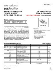
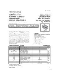
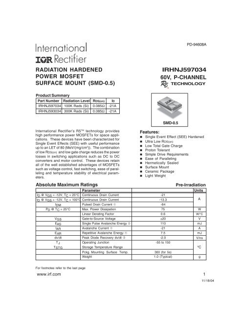
PD-94608ARADIATION HARDENEDPOWER MOSFETSURFACE MOUNT (SMD-0.5)IRHNJ59703460V, P-CHANNEL5 TECHNOLOGYProduct SummaryPart Number Radiation Level RDS(on) IDIRHNJ597034 100K Rads (Si) 0.085Ω -21AIRHNJ593034 300K Rads (Si) 0.085Ω -21AInternational Rectifier’s R5 TM technology provideshigh performance <strong>power</strong> MOSFETs for space applications.These devices have been characterized forSingle Event Effects (SEE) with useful performanceup to an LET of 80 (MeV/(mg/cm 2 )). The combinationof low RDS(on) and low gate charge reduces the <strong>power</strong>losses in switching applications such as DC to DCconverters and motor control. These devices retainall of the well established advantages of MOSFETssuch as voltage control, fast switching, ease of parallelingand temperature stability of electrical parameters.Absolute Maximum RatingsParameterID @ VGS = -12V, TC = 25°C Continuous Drain Current -21ID @ VGS = -12V, TC = 100°C Continuous Drain Current -13.3IDM Pulsed Drain Current À -84SMD-0.5Features:n Single Event Effect (SEE) Hardenedn Ultra Low RDS(on)n Low Total Gate Chargen Proton Tolerantn Simple Drive Requirementsn Ease of Parallelingn Hermetically Sealedn Surface Mountn Ceramic Packagen Light WeightPre-Ir<strong>radiation</strong>UnitsPD @ TC = 25°C Max. Power Dissipation 75 WLinear Derating Factor 0.6 W/°CVGS Gate-to-Source Voltage ±20 VEAS Single Pulse Avalanche Energy Á 110 mJIAR Avalanche Current À -21 AEAR Repetitive Avalanche Energy À 7.5 mJdv/dt Peak Diode Recovery dv/dt  -2.0 V/nsTJ Operating Junction -55 to 150TSTGStorage Temperature RangePckg. Mounting Surface Temp. 300 (for 5s)o CWeight 1.0 (Typical) gAFor footnotes refer to the last pagewww.irf.com 111/18/04
IRHNJ597034Pre-Ir<strong>radiation</strong>Electrical Characteristics @ Tj = 25°C (Unless Otherwise Specified)Parameter Min Typ Max Units Test ConditionsBVDSS Drain-to-Source Breakdown Voltage -60 — — V VGS = 0V, ID = -1.0mA∆BVDSS/∆TJ Temperature Coefficient of Breakdown — 0.063 — V/°C Reference to 25°C, ID = -1.0mAVoltageRDS(on) Static Drain-to-Source On-State — — 0.085 Ω VGS = -12V, ID = -13.3AÃResistanceVGS(th) Gate Threshold Voltage -2.0 — -4.0 V VDS = VGS, ID = -1.0mAgfs Forward Transconductance 10 — — S ( ) VDS = -25V, IDS = -13.3A ÃIDSS Zero Gate Voltage Drain Current — — -10 VDS= -48V ,VGS=0VµA— — -25 VDS = -48V,VGS = 0V, TJ =125°CIGSS Gate-to-Source Leakage Forward — — -100 VGS = -20VnAIGSS Gate-to-Source Leakage Reverse — — 100 VGS = 20VQg Total Gate Charge — — 45 VGS =-12V, ID = -21AQgs Gate-to-Source Charge — — 18 nC VDS = -30VQgd Gate-to-Drain (‘Miller’) Charge — — 13td(on) Turn-On Delay Time — — 25 VDD = -30V, ID = -21A,tr Rise Time — — 65 VGS =-12V, RG = 7.5Ω,nstd(off) Turn-Off Delay Time — — 75tf Fall Time — — 50LS + LD Total Inductance — 4.0 — nH Measured from the center ofdrain pad to center of source padCiss Input Capacitance — 1540 — VGS = 0V, VDS = -25VCoss Output Capacitance — 590 — pF f = 1.0MHzCrss Reverse Transfer Capacitance — 60 —ΩSource-Drain Diode Ratings and CharacteristicsParameter Min Typ Max Units Test ConditionsIS Continuous Source Current (Body Diode) — — -21ISM Pulse Source Current (Body Diode) À — — -84AVSD Diode Forward Voltage — — -5.0 V Tj = 25°C, IS = -21A, VGS = 0V Ãtrr Reverse Recovery Time — — 100 ns Tj = 25°C, IF = -21A, di/dt ≤ -100A/µsQRR Reverse Recovery Charge — — 200 nC VDD ≤ -25V Ãton Forward Turn-On Time Intrinsic turn-on time is negligible. Turn-on speed is substantially controlled by LS + LD.Thermal ResistanceParameter Min Typ Max Units Test ConditionsRthJC Junction-to-Case — — 1.67°C/WRthJ-PCB Junction-to-PC board — 6.9 — soldered to a 2” square copper-clad boardNote: Corresponding Spice and Saber models are available on International Rectifier website.For footnotes refer to the last page2 www.irf.com
-I SD , Reverse Drain Current ( Α)-I D , Drain-to-Source Current (A)C, Capacitance (pF)-V GS , Gate-to-Source Voltage (V)Pre-Ir<strong>radiation</strong>IRHNJ59703425002000CissV GS = 0V, f = 1 MHZC iss= C gs+ C gd, C dsSHORTEDC rss= C gd1612I D = -21AV DS = -48VV DS = -30VVDS= -12V1500Coss8100050040Crss1 10 1000C oss= C ds+ C gd0 5 10 15 20 25 30FOR TEST CIRCUITSEE FIGURE 13-V DS , Drain-to-Source Voltage (V)Q G Total Gate Charge (nC)Fig 5. Typical Capacitance Vs.Drain-to-Source VoltageFig 6. Typical Gate Charge Vs.Gate-to-Source Voltage1001000100OPERATION IN THIS AREALIMITED BY R DS (on)10T J = 25°CT J = 150°C10100µsV GS = 0V1.00.5 1.5 2.5 3.5 4.5 5.5 6.5-V SD , Source-to-Drain Voltage (V)1Tc = 25°CTj = 150°CSingle Pulse1ms10ms1 10 100 1000-V DS , Drain-to-Source Voltage (V)Fig 7. Typical Source-Drain DiodeForward VoltageFig 8. Maximum Safe Operating Areawww.irf.com 5
-I D ,Drain Current (A)IRHNJ597034Pre-Ir<strong>radiation</strong>24V DSR D2016R GV GSD.U.T.+-V DD12V GSPulse Width ≤ 1 µsDuty Factor ≤ 0.1 %8Fig 10a. Switching Time Test Circuit4025 50 75 100 125 150T C , Case Temperature (°C)Fig 9. Maximum Drain Current Vs.Case Temperaturet d(on) t r t d(off) t f10%90%V DSFig 10b. Switching Time Waveforms10Thermal Response (Z thJC )10.1D = 0.500.200.100.050.020.01SINGLE PULSE(THERMAL RESPONSE)Notes:1. Duty factor D = t 1 / t 20.012. Peak T J= P DM x Z thJC + TC0.00001 0.0001 0.001 0.01 0.1 1t 1, Rectangular Pulse Duration (sec)PDMt1t2Fig 11. Maximum Effective Transient Thermal Impedance, Junction-to-Case6 www.irf.com
E AS , Single Pulse Avalanche Energy (mJ)Pre-Ir<strong>radiation</strong>IRHNJ597034V DSLR G D.U.T-V DDI +ASA-20V V GSDRIVERtp 0.01Ω15VI ASFig 12a. Unclamped Inductive Test Circuit20016012080400I DTOP -9.4A-13.3ABOTTOM -21A25 50 75 100 125 150Starting T J , Junction Temperature (°C)Fig 12c. Maximum Avalanche EnergyVs. Drain CurrenttpV (BR)DSSFig 12b. Unclamped Inductive WaveformsCurrent RegulatorSame Type as D.U.T.-12 VQ GSQ GQ GD-12V.2µF50KΩ.3µFD.U.T.-+ V DSV GV GS-3mAChargeI G I DCurrent Sampling ResistorsFig 13a. Basic Gate Charge WaveformFig 13b. Gate Charge Test Circuitwww.irf.com 7
IRHNJ597034Pre-Ir<strong>radiation</strong>Footnotes:À Repetitive Rating; Pulse width limited bymaximum junction temperature.Á VDD = - 25V, starting TJ = 25°C, L=0.5mHPeak IL = - 21A, VGS = -12VÂ ISD ≤ - 21A, di/dt ≤ - 435A/µs,VDD ≤ - 60V, TJ ≤ 150°CÃ Pulse width ≤ 300 µs; Duty Cycle ≤ 2%Ä Total Dose Ir<strong>radiation</strong> with VGS Bias.-12 volt VGS applied and VDS = 0 duringir<strong>radiation</strong> per MIL-STD-750, method 1019, condition A.Å Total Dose Ir<strong>radiation</strong> with VDS Bias.-48 volt VDS applied and VGS = 0 duringir<strong>radiation</strong> per MlL-STD-750, method 1019, condition A.Case Outline and Dimensions — SMD-0.5PAD ASSIGNMENTS1 = DRAIN2 = GATE3 = SOURCEIR WORLD HEADQUARTERS: 233 Kansas St., El Segundo, California 90245, USA Tel: (310) 252-7105IR LEOMINSTER : 205 Crawford St., Leominster, Massachusetts 01453, USA Tel: (978) 534-5776TAC Fax: (310) 252-7903Visit us at www.irf.com for sales contact information.Data and specifications subject to change without notice. 11/20048 www.irf.com