Automotive Grade AUIR2085S - International Rectifier
Automotive Grade AUIR2085S - International Rectifier
Automotive Grade AUIR2085S - International Rectifier

Create successful ePaper yourself
Turn your PDF publications into a flip-book with our unique Google optimized e-Paper software.
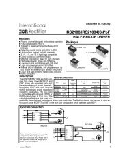
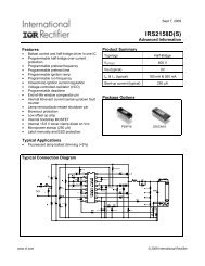
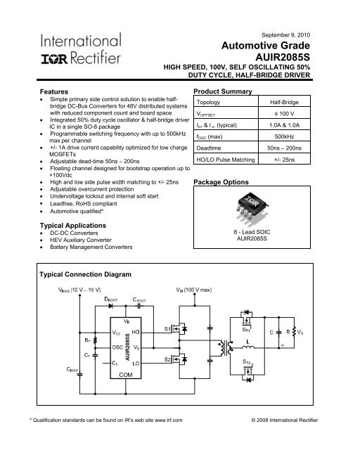
September 9, 2010<strong>Automotive</strong> <strong>Grade</strong><strong>AUIR2085S</strong>HIGH SPEED, 100V, SELF OSCILLATING 50%DUTY CYCLE, HALF-BRIDGE DRIVERFeatures• Simple primary side control solution to enable halfbridgeDC-Bus Converters for 48V distributed systemswith reduced component count and board space• Integrated 50% duty cycle oscillator & half-bridge driverIC in a single SO-8 package• Programmable switching frequency with up to 500kHzmax per channel• +/- 1A drive current capability optimized for low chargeMOSFETs• Adjustable dead-time 50ns – 200ns• Floating channel designed for bootstrap operation up to+100Vdc• High and low side pulse width matching to +/- 25ns• Adjustable overcurrent protection• Undervoltage lockout and internal soft start• Leadfree, RoHS compliant• <strong>Automotive</strong> qualified*Typical Applications• DC-DC Converters• HEV Auxiliary Converter• Battery Management ConvertersProduct SummaryTopologyV OFFSETHalf-Bridge≤ 100 VI o+ & I o- (typical) 1.0A & 1.0Af OSC (max)DeadtimeHO/LO Pulse MatchingPackage Options8 - Lead SOIC<strong>AUIR2085S</strong>500kHz50ns – 200ns+/- 25nsTypical Connection DiagramAUIRS2085<strong>AUIR2085S</strong>COM* Qualification standards can be found on IR’s web site www.irf.com © 2008 <strong>International</strong> <strong>Rectifier</strong>
<strong>AUIR2085S</strong>Table of ContentsPageTypical Connection Diagram 1Description/Feature Comparison 3Qualification Information 4Absolute Maximum Ratings 5Recommended Operating Conditions 5Dynamic Electrical Characteristics 6Static Electrical Characteristics 6Functional Block Diagram 7Input/Output Pin Equivalent Circuit Diagram 9Lead Definitions 10Lead Assignments 10Package Details 12Tape and Reel Details 13Part Marking Information 14Ordering Information 15www.irf.com2© 2008 <strong>International</strong> <strong>Rectifier</strong>
<strong>AUIR2085S</strong>Qualification Information †Qualification LevelMoisture Sensitivity LevelESDMachine ModelHuman Body ModelCharged Device ModelIC Latch-Up TestRoHS Compliant<strong>Automotive</strong>(per AEC-Q100 †† )Comments: This family of ICs has passed an <strong>Automotive</strong>qualification. IR’s Industrial and Consumer qualification levelis granted by extension of the higher <strong>Automotive</strong> level.MSL3 ††† 260°CSOIC8N(per IPC/JEDEC J-STD-020)Class M2 (+/-200V)(per AEC-Q100-003)Class H1B (+/-1750V)(per AEC-Q100-002)Class C4 (+/-1000V)(per AEC-Q100-011)Class II, Level B(per AEC-Q100-004)Yes† Qualification standards can be found at <strong>International</strong> <strong>Rectifier</strong>’s web site http://www.irf.com/†† Exceptions to AEC-Q100 requirements are noted in the qualification report.††† Higher MSL ratings may be available for the specific package types listed here. Please contact your<strong>International</strong> <strong>Rectifier</strong> sales representative for further information.www.irf.com4© 2008 <strong>International</strong> <strong>Rectifier</strong>
<strong>AUIR2085S</strong>Dynamic Electrical CharacteristicsV CC = V BS = 12V, C LOAD = 1000pF, and T A = 25°C unless otherwise specified.Symbol Definition Min Typ Max Units Test Conditionst r Turn-on rise time — 40 60t f Turn-off fall time — 20 30ns V S = 0Vf OSC Per channel output frequency 500 — — kHz C T = 100pF,t DT HO/LO output dead time 50 — —R T = 10kΩt DCS Overcurrent shut down delay — 200 — ns Pulse on C SPM HO/LO pulse width mismatch -25 — 25V S = 0V ~ 100VStatic Electrical CharacteristicsV CC = V BS = 12V, C LOAD = 1000pF, and T A = 25°C unless otherwise specified.Symbol Definition Min Typ Max Units Test ConditionsV OH High level output voltage, V CC or V BS – V O — — 1.5V OL Low level output voltage — — 0.1I Ieak Offset supply leakage current — — 50I QBS Quiescent V BS supply current — — 150I QCC Quiescent V CC supply current — — 1.5 mAV CS+ Overcurrent shutdown threshold 250 300 350 mVV CS- Overcurrent shutdown threshold 150 200 250 mVV CCUV+ Undervoltage positive going threshold 6.8 7.3 7.8V CCUV- Undervoltage negative going threshold 6.3 6.8 7.3V BSUV+High side undervoltage positive goingthreshold6.8 7.3 7.8V BSUV-High side undervoltage negative goingthreshold6.3 6.8 7.3I O+ Output high short circuit current — 1.0 —I O- Output low short circuit current — 1.0 —VµAVAwww.irf.com6© 2008 <strong>International</strong> <strong>Rectifier</strong>
<strong>AUIR2085S</strong>Functional Block Diagram<strong>AUIR2085S</strong>COMwww.irf.com7© 2008 <strong>International</strong> <strong>Rectifier</strong>
<strong>AUIR2085S</strong>www.irf.com8© 2008 <strong>International</strong> <strong>Rectifier</strong>
<strong>AUIR2085S</strong>Input/Output Pin Equivalent Circuit DiagramsV CCESDDiodeESDDiodeCSESDDiodeR ESDESDDiodeCOMwww.irf.com9© 2008 <strong>International</strong> <strong>Rectifier</strong>
<strong>AUIR2085S</strong>Lead DefinitionsPIN Symbol Description1 CS Current sense input2 OSC Oscillator pin3 COM Logic supply return4 LO Low side output5 V CC Logic supply6 V S Floating supply return7 HO High side output8 V B High side floating supplyLead Assignmentswww.irf.com10© 2008 <strong>International</strong> <strong>Rectifier</strong>
<strong>AUIR2085S</strong>Pin DescriptionsCs: The input pin to the overcurrent comparator. Exceeding the overcurrent threshold value specified in“Static Electrical Parameters” Section will terminate output pulses and start a new soft start cycle as soon asthe voltage on the pin reduce below the threshold value.OSC: The oscillator-programming pin. Only two components are required to program the internal oscillatorfrequency: a resistor connected between the V CC pin and the OSC pin, and a capacitor connected from theOSC to COM. The approximate oscillator frequency is determined by the following simple formula:f OSC = 1 / (2 · R T · C T )Where frequency is in Hertz (Hz), RT resistance in Ohms (Ω) and CT capacitance in Farads (F). Therecommended range of timing resistors is between 10kΩ and 100kΩ and range of time capacitances isbetween 47pF and 470pF. The timing resistors less than 10kΩ should be avoided. The value of the timingcapacitor determines the amount of dead time between the two output drivers: lower the CT, shorter thedead time and vice versa. It is not recommended to use a timing capacitor below 47pF, for best performancekeep the timing components physically as close as possible to the <strong>AUIR2085S</strong>. Separated ground and V CCtraces to the timing components are encouraged.COM: Signal ground and power ground for all functions. Due to high current and high frequency operation, alow impedance circuit board ground plane is highly recommended.HO, LO: High side and low side gate drive pins. The high and low side drivers can directly drive the gate of apower MOSFET. The drivers are capable of 1A peak source and sink currents. It is recommended that thehigh and low drive pins be very close to the gates of the high side and low side MOSFETs to prevent anydelay and distortion of the drive signals.V B : The high side power input connection. The high side supply is derived from a bootstrap circuit using alow-leakage Schottky diode and a ceramic capacitor. To prevent noise, the Schottky diode and bypasscapacitor should be very close to the <strong>AUIR2085S</strong>.V S : The high side power return connection. V S should be connected directly to the source terminal of highside MOSFET with a trace as short as possible.V CC : The IC bias input connection for the device. Although the quiescent V CC current is very low, total supplycurrent will be higher, depending on the gate charge of the MOSFETs connected to the HO and LO pins, andthe programmed oscillator frequency, total V CC current is the sum of quiescent V CC current and the averagecurrent at HO and LO. Knowing the operating frequency and the MOSFET gate charge (Qg) at selected V CCvoltage, the average current can be calculated from:Iave = 2 x Qg X f OSCTo prevent noise problem, a bypass ceramic capacitor connected to V CC and COM should be placed asclose as possible to the <strong>AUIR2085S</strong>.<strong>AUIR2085S</strong> has an under voltage lookout feature for the IC bias supply, V CC . The minimum voltage requiredon V CC to make sure that IC will work within specifications must be higher than 8.5V (10V minimum V CC isrecommended to prevent asymmetrical gates signal on HO and LO pins that are expected when V CC isbetween 7.5V and 8.5V).www.irf.com11© 2008 <strong>International</strong> <strong>Rectifier</strong>
<strong>AUIR2085S</strong>Tape and Reel Details:LOADED TAPE FEED DIRECTIONBAHDFCNOTE : CONTROLLINGDIMENSION IN MMEGCARRIER TAPE DIMENSION FOR 8SOICNMetricImperialCode Min Max Min MaxA 7.90 8.10 0.311 0.318B 3.90 4.10 0.153 0.161C 11.70 12.30 0.46 0.484D 5.45 5.55 0.214 0.218E 6.30 6.50 0.248 0.255F 5.10 5.30 0.200 0.208G 1.50 n/a 0.059 n/aH 1.50 1.60 0.059 0.062FDECBAGHREEL DIMENSIONS FOR 8SOICNMetricImperialCode Min Max Min MaxA 329.60 330.25 12.976 13.001B 20.95 21.45 0.824 0.844C 12.80 13.20 0.503 0.519D 1.95 2.45 0.767 0.096E 98.00 102.00 3.858 4.015F n/a 18.40 n/a 0.724G 14.50 17.10 0.570 0.673H 12.40 14.40 0.488 0.566www.irf.com13© 2008 <strong>International</strong> <strong>Rectifier</strong>
<strong>AUIR2085S</strong>Part Marking Informationwww.irf.com14© 2008 <strong>International</strong> <strong>Rectifier</strong>
<strong>AUIR2085S</strong>Ordering InformationBase Part NumberPackage TypeStandard PackFormQuantityComplete Part Number<strong>AUIR2085S</strong>SOIC8Tube/Bulk 95 <strong>AUIR2085S</strong>Tape and Reel 2500 <strong>AUIR2085S</strong>TRThe information provided in this document is believed to be accurate and reliable. However, <strong>International</strong> <strong>Rectifier</strong> assumes noresponsibility for the consequences of the use of this information. <strong>International</strong> <strong>Rectifier</strong> assumes no responsibility for anyinfringement of patents or of other rights of third parties which may result from the use of this information. No license is granted byimplication or otherwise under any patent or patent rights of <strong>International</strong> <strong>Rectifier</strong>. The specifications mentioned in this document aresubject to change without notice. This document supersedes and replaces all information previously supplied.For technical support, please contact IR’s Technical Assistance Centerhttp://www.irf.com/technical-info/WORLD HEADQUARTERS:233 Kansas St., El Segundo, California 90245Tel: (310) 252-7105Revision Historywww.irf.com15© 2008 <strong>International</strong> <strong>Rectifier</strong>
<strong>AUIR2085S</strong>DateComment5/8/08 Created <strong>AUIR2085S</strong> based on IR2085SChanged all references to the AUIRS2085S (Gen5) to <strong>AUIR2085S</strong> (Gen2)Changed all GND references to COM in text/diagramsSeveral changes to the product summaryChanged topology from “3 Phase” to “Half-Bridge”Changed V OFFSET from 600V to 100VRemoved V OUT referenceIncluded f OSC(max) of 500kHzUpdated Deadtime range, 50ns – 200nsIncluded HO/LO Pulse Width Matching of +/- 25nsRemoved “Typical Applications” section8/21/08Changed dV S /dt spec from +/- 50V to just 50V maxUpdated P D max from 1W to 0.625WRemoved T J min spec to be consistent with other datasheetsChanged recommended V B spec from V DD - 0.7V/15V to V S + 10V/V S + 15VChanged recommended T J spec to T ARenamed UV CC+ to V CCUV+Renamed UV CC- to V CCUV-Renamed UV BS+ to V BSUV+Renamed UV BS- to V BSUV-Added IC label on lead assignment blockAdded ESD/LU ratings to qual table12/5/08 Corrected lead assignment dwg (Vs and HO were swapped)Edited lead assignment dwg to align with templateChange from APBU:12/11/08 Added typ application diagram on the first page. Moved typ connection diagram, it from frontpage to page 3.Change from APBU:1/22/09 Removed Typ App Diagram and moved Typ connection diagram back to P1.Added Typical Applications on P11/28/09 Scott reviewed the datasheet, Preliminary sign removed1/29/09 Parameter Temperature trends removedmax Timing Capacitor Rec. Op. Cond. Changed from 1000 pF to 470pF.2/6/09 Fig.1,Fig2 and Fig3 added, copied back from IR2085SAdded details to soft start description.Removed P12 (application information)7/13/09Updated table of contents (renumbering)9/8/2010 Updated ESD classificationwww.irf.com16© 2008 <strong>International</strong> <strong>Rectifier</strong>