IRS2108-IRS21084 (S)PbF
IRS2108-IRS21084 (S)PbF
IRS2108-IRS21084 (S)PbF

Create successful ePaper yourself
Turn your PDF publications into a flip-book with our unique Google optimized e-Paper software.
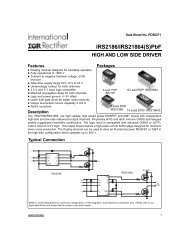
(Refer to Lead Assignments for correct pinconfiguration). These diagrams show electrical connections only. Please refer to Data Sheet No. PD60260<strong>IRS2108</strong>/<strong>IRS2108</strong>4(S)<strong>PbF</strong>FeaturesHALF-BRIDGE DRIVER• Floating channel designed for bootstrap operation Packages• Fully operational to +600 V• Tolerant to negative transient voltage, dV/dtimmune8-Lead PDIP• Gate drive supply range from 10 V to 20 V• Undervoltage lockout for both channels14-Lead PDIP• 3.3 V, 5 V, and 15 V input logic compatible• Cross-conduction prevention logic• Matched propagation delay for both channels•High-side output in phase with HIN input•Low-side output out of phase with input• Logic and power ground +/- 5 V offset•Internal 540 ns deadtime, and programmable up8-Lead SOIC14-Lead SOICto 5 µs with one external R DT resistor (<strong>IRS2108</strong>4)•Lower di/dt gate driver for better noise immunity•RoHS compliantDescriptionFeature ComparisonThe <strong>IRS2108</strong>/<strong>IRS2108</strong>4 are high voltage,high speed power MOSFET and ton/toffIGBT drivers with dependent high- and low-side referenced output channels.Proprietary HVIC and latch immune CMOS technologies enable ruggedized monolithic construction. The logic input is compatible with standard CMOS or LSTTL output, down to 3.3 V logic. The output drivers feature a high pulse currentbuffer stage designed for minimum driver cross-conduction. The floating channel can be used to drive anN-channel power MOSFET or IGBT in the high-side configuration which operates up to 600 V.Typical Connection <strong>IRS2108</strong>4<strong>IRS2108</strong> our Application Notes and DesignTips forproper circuit board layout.www.irf.com 1
<strong>IRS2108</strong>/<strong>IRS2108</strong>4(S)<strong>PbF</strong>Absolute Maximum RatingsAbsolute maximum ratings indicate sustained limits beyond which damage to the device may occur. All voltage parametersare absolute voltages referenced to COM. The thermal resistance and power dissipation ratings are measuredunder board mounted and still air conditions.Symbol Definition Min. Max. UnitsV B High-side floating absolute voltage -0.3 625V S High-side floating supply offset voltage V B - 25 V B + 0.3V HO High-side floating output voltage V S - 0.3 V B + 0.3V CC Low-side and logic fixed supply voltage -0.3 25V LO Low-side output voltage -0.3 V CC + 0.3DT Programmable deadtime pin voltage (<strong>IRS2108</strong>4 only) V SS - 0.3 V CC + 0.3V IN Logic input voltage (HIN & ) V SS - 0.3 V CC + 0.3V SS Logic ground (<strong>IRS2108</strong>4 only ) V CC - 25 V CC + 0.3dV S /dt Allowable offset supply voltage transient — 50 V/ns(8 lead PDIP) — 1.0(8 lead SOIC) — 0.625P D Package power dissipation @ TA ≤ +25 o C(14 lead PDIP) — 1.6(14 lead SOIC) — 1.0(8 lead PDIP) — 125RthJA Thermal resistance, junction to ambient(8 lead SOIC) — 200(14 lead PDIP) — 75(14 lead SOIC) — 120T J Junction temperature — 150T S Storage temperature -50 150T L Lead temperature (soldering, 10 seconds) — 300VW°C/W°CRecommended Operating ConditionsThe input/output logic timing diagram is shown in Fig. 1. For proper operation the device should be used within therecommended conditions. The V S and V SS offset rating are tested with all supplies biased at a 15 V differential.Symbol Definition Min. Max. UnitsVB High-side floating supply absolute voltage V S + 10 V S + 20V S High-side floating supply offset voltage Note 1 600V HO High-side floating output voltage V S V BV CC Low-side and logic fixed supply voltage 10 20V LO Low-side output voltage 0 V CCV<strong>IRS2108</strong> COM V CCV IN Logic input voltage<strong>IRS2108</strong>4 V SS V CCDT Programmable deadtime pin voltage (<strong>IRS2108</strong>4 only) V S V CCV SS Logic ground (<strong>IRS2108</strong>4 only ) -5 5T A Ambient temperature -40 125 °CNote 1: Logic operational for V S of -5 V to +600 V. Logic state held for V S of -5 V to -V BS . (Please refer to the Design TipDT97-3 for more details).www.irf.com 2
<strong>IRS2108</strong>/<strong>IRS2108</strong>4(S)<strong>PbF</strong>Dynamic Electrical CharacteristicsV BIAS (V CC , V BS ) = 15 V, V SS = COM, C L = 1000 pF, T A = 25 °C, DT = V SS unless otherwise specified.Symbol Definition Min. Typ. Max. Units Test Conditionston Turn-on propagation delay — 220 300 VS = 0 Vtoff Turn-off propagation delay — 200 280 V S = 0 V or 600 VMT Delay matching | ton - toff | — 0 30tr Turn-on rise time — 100 220tf Turn-off fall time — 35 80DTDeadtime: LO turn-off to HO turn-on(DTLO-HO) & 400 540 680 R DT = 0 ΩHO turn-off to LO turn-on (DTHO-LO) 4 5 6 µs R DT = 200 kΩ (IR21084)MDT Deadtime matching = | DTLO-HO - DTHO-LO |nsV S = 0 V— 0 60 ns R DT =0 Ω— 0 600 R DT = 200 kΩ (IR21084)Static Electrical CharacteristicsV BIAS (V CC , V BS ) = 15 V, V SS = COM, DT= V SS and T A = 25 °C unless otherwise specified. The V IL , V IH, and I INparameters are referenced to V SS /COM and are applicable to the respective input leads: HIN and LIN. The V O , I O, andRon parameters are referenced to COM and are applicable to the respective output leads: HO and LO.Symbol Definition Min. Typ. Max. Units Test ConditionsV IH Logic “1” input voltage for HIN & logic “0” for 2.5 — —V IL Logic “0” input voltage for HIN & logic “1” for — — 0.8V OH High level output voltage, V BIAS - V O — 0.05 0.2V OL Low level output voltage, V O — 0.02 0.1I LK Offset supply leakage current — — 50 V B = V S = 600 VI QBS Quiescent V BS supply current 20 75 130µAV IN = 0 V or 5 VI QCC Quiescent VCC supply current 0.4 1.0 1.6 mAV IN = 0 V or 5 VRDT=0 ΩI IN+ Logic “1” input bias current — 5 20 HIN = 5 V, = 0 VI IN- Logic “0” input bias current — — 5µAHIN = 0 V, = 5 VV CCUV+V BSUV+V CCUV-V BSUV-V CC and V BS supply undervoltage positive goingthresholdV CC and V BS supply undervoltage negative goingthreshold8.0 8.9 9.87.4 8.2 9.0V CCUVHHysteresis 0.3 0.7 —VVV CC = 10 V to 20 VI O = 2 mAV BSUVHIO+ Output high short circuit pulsed current 120 290 —IO- Output low short circuit pulsed current 250 600 —mAV O = 0 V,PW ≤ 10 µsV O = 15 V,PW ≤ 10 µswww.irf.com 3
www.irf.com 4<strong>IRS2108</strong>/<strong>IRS2108</strong>4(S)<strong>PbF</strong>Functional Block Diagram21084LIN+5VUVDETECTDELAYCOMLOVCCHINDTVSSVSHOVBPULSEFILTERHVLEVELSHIFTERRRSQUVDETECTDEADTIME &SHOOT-THROUGHPREVENTIONPULSEGENERATORVSS/COMLEVELSHIFTVSS/COMLEVELSHIFT2108LIN+5VUVDETECTDELAYCOMLOVCCHINDTVSSVSHOVBPULSEFILTERHVLEVELSHIFTERRRSQUVDETECTDEADTIME &SHOOT-THROUGHPREVENTIONPULSEGENERATORVSS/COMLEVELSHIFTVSS/COMLEVELSHIFT
<strong>IRS2108</strong>/<strong>IRS2108</strong>4(S)<strong>PbF</strong>Lead DefinitionsSymbol DescriptionHINDTVSSV BHOV SV CCLOCOMLogic input for high-side gate driver output (HO), in phase (referenced to COM for <strong>IRS2108</strong>and VSS for <strong>IRS2108</strong>4)Logic input for low-side gate driver output (LO), out of phase (referenced to COM for <strong>IRS2108</strong>and VSS for <strong>IRS2108</strong>4)Programmable deadtime lead, referenced to VSS (IR21084 only)Logic ground (<strong>IRS2108</strong>4 only)High-side floating supplyHigh-side gate driver outputHigh-side floating supply returnLow-side and logic fixed supplyLow-side gate driver outputLow-side returnLead Assignments1V CCV B81V CCV B82HINHO72HINHO73LINV S63LINV S64COMLO54COMLO58 Lead PDIP 8 Lead SOIC<strong>IRS2108</strong><strong>PbF</strong><strong>IRS2108</strong>S<strong>PbF</strong>1234V CCHINLINDTV BHOV S141312111234V CCHINLINDTV BHOV S141312115VSS105VSS106COM96COM97LO87LO814 Lead PDIP 14 Lead SOIC<strong>IRS2108</strong>4<strong>PbF</strong><strong>IRS2108</strong>4S<strong>PbF</strong>www.irf.com 5
<strong>IRS2108</strong>/<strong>IRS2108</strong>4(S)<strong>PbF</strong>Figure 1. Input/Output Timing Diagram Figure 2. Switching Time Waveform Definitions Figure 3. Deadtime Waveform Definitionswww.irf.com 6
<strong>IRS2108</strong>/<strong>IRS2108</strong>4(S)<strong>PbF</strong>Turn-On Propagation Delay (ns)500400300M ax.200Typ.1000-50 -25 0 25 50 75 100 125Turn-On Propagation Delay (ns)500400M ax.300Typ.200100010 12 14 16 18 20Temperature ( o C)V BIASSupply Voltage (V)Figure 4A. Turn-On Propagation Delayvs. TemperatureFigure 4B. Turn-On Propagation Delayvs. Supply VoltageTurn-Off Propagation Delay (ns)500400300M ax.200Typ.1000-50 -25 0 25 50 75 100 125Turn-Off Propagation Delay (ns)500400M ax.300Typ.200100010 12 14 16 18 20Temperature ( o C)V BIASSupply Voltage (V)Figure 5A. Turn-Off Propagation Delayvs.TemperatureFigure 5B. Turn-Off Propagation Delayvs. Supply Voltagewww.irf.com 7
<strong>IRS2108</strong>/<strong>IRS2108</strong>4(S)<strong>PbF</strong>)500500Turn-On Rise Time (ns4003002001000Max.Typ.Turn-On Rise Time (ns4003002001000-50 -25 0 25 50 75 100 12510 12 14 16 18 20Temperature ( o C)V BIAS Supply Voltage (V)Figure 6A. Turn-On Rise Timevs.Temperature)Max.Typ.Figure 6B. Turn-On Rise Timevs. Supply Voltage200200)Turn-Off Fall Time (ns)150100500Turn-Off Turn-Off Fall Time Fall Time (ns)150100500-50 -25 0 25 50 75 100 12510 12 14 16 18 20Temperature ( o C)Input Voltage (V)Figure 7A. Turn-Off Fall Timevs. TemperatureFigure 7B. Turn-Off Fall Timevs. Input voltagewww.irf.com 8
<strong>IRS2108</strong>/<strong>IRS2108</strong>4(S)<strong>PbF</strong>10001000Deadtime (ns)800600400Max.Typ.Min.Deadtime (ns)800600400Max.Typ.Min.200-50 -25 0 25 50 75 100 12520010 12 14 16 18 20Temperature ( o C)V BIASSupply Voltage (V)Figure 8A. Deadtime vs. TemperatureFigure 8B. Deadtime vs. Supply Voltage7867Deadtime (µs) ( 5432Max.Typ.Min.Input Voltage (V)65432Min.11000 50 100 150 200-50 -25 0 25 50 75 100 125R DT(kΩ)Temperature ( o C)Figure 8C. Deadtime vs. R DT(IR21084 Only)Figure 9A. Logic "1" Input Voltagevs. Temperaturewww.irf.com 9
<strong>IRS2108</strong>/<strong>IRS2108</strong>4(S)<strong>PbF</strong>84.0Input Voltage (V)7654321Min.Input Voltage (V)3.22.41.60.8Min.00.010 12 14 16 18 20-50 -25 0 25 50 75 100 125V BAISSupply Voltage (V)Temperature ( o C)Figure 9B. Logic "1" Input Voltagevs. Supply VoltageFigure 10A. Logic "0" Input Voltagevs. TemperatureInput Voltage (V)4.03.22.41.60.8Min.0.010 12 14 16 18 20)High Level Output Voltage (V0.50.40.30.20.10.0Max.Typ.-50 -25 0 25 50 75 100 125V CCSupply Voltage (V)Temperature ( o C)Figure 10B. Logic "0" Input Voltagevs. Supply VoltageFigure 11A. High Level Output Voltagevs. Temperaturewww.irf.com 10
<strong>IRS2108</strong>/<strong>IRS2108</strong>4(S)<strong>PbF</strong>)High Level Output Voltage (V0.50.40.30.20.1Max.Typ.0.010 12 14 16 18 20V BAISSupply Voltage (V)Figure 11B. High Lovel Output Voltagevs. Supply VoltageLow Level Output Voltage (V)0.50.40.30.20.1Max.Typ.0.0-50 -25 0 25 50 75 100 125Temperature ( o C)Figure 12A. Low Level Output Voltagevs.TemperatureLow Level Output Voltage (V)0.50.40.30.2Max.0.1Typ.010 12 14 16 18 20V BIASSupply Voltage (V)Offset Supply Leakage Current ( (µA)500400300200100M ax.0-50 -25 0 25 50 75 100 125Temperature ( o C)Figure 12B. Low Level Output Voltagevs. Supply VoltageFigure 13A. Offset Supply Leakage Currentvs. Temperaturewww.irf.com 11
<strong>IRS2108</strong>/<strong>IRS2108</strong>4(S)<strong>PbF</strong>Offset Supply Leakage Current (µA) ( 500400300200100M ax.00 100 200 300 400 500 600V BBoost Voltage (V)V BSSupply Current (µA) ( 400300200100M ax.Typ.Min.0-50 -25 0 25 50 75 100 125Temperature ( o C)Figure 13B. Offset Supply Leakage Currentvs. TemperatureFigure 14A. V BSSupply Currentvs. Temperature4003.0V BSSupply Current (µA) ( 300200M ax.100Typ.Min.010 12 14 16 18 20V BSSupply Voltage (V)V CCSupply Current (mA)2.52.0M ax.1.5Typ.1.0Min.0.50.0-50 -25 0 25 50 75 100 125Temperature ( o C)Figure 14B. V BSSupply Currentvs. Supply VoltageFigure 15A. V CCSupply Currentvs. Temperaturewww.irf.com 12
<strong>IRS2108</strong>/<strong>IRS2108</strong>4(S)<strong>PbF</strong>3.060V CCSupply Current (mA)2.52.01.51.00.50.0Max.Typ.Min.10 12 14 16 18 20V CCSupply Voltage (V)L o g i c " 1 " I n p u t C u r r e n t ( (µA) A )50403020100Max.Typ.-50 -25 0 25 50 75 100 125Temperature ( o C)Figure 15B. V CCSupply Currentvs. Supply VoltageFigure 16A. Logic "1" Input Currentvs. TemperatureLogic "1" Input Current (µA)6050403020100Max.Typ.10 12 14 16 18 20V CCSupply Voltage (V)Figure 16B. Logic "1" Input Currentvs. Supply VoltageLogic "0" Input Bias Current (µA)65 Max43210-50 -25 0 25 50 75 100 125Temperature (°C)Figure 17A. Logic "0" Input Bias Currentvs. Temperaturewww.irf.com 13
<strong>IRS2108</strong>/<strong>IRS2108</strong>4(S)<strong>PbF</strong>Logic "0" Input Bias Current (µA)6543210Max10 12 14 16 18 20V CCUVLO Threshold (+) (V)121110987Max.Typ.Min.-50 -25 0 25 50 75 100 125Supply Voltage (V)Temperature ( o C)Figure 17B. Logic "0" Input Bias CurrentFigure 17B. Logic "0" Input Bias Currentvs. VoltageFigure 18. V CCUndervoltage Threshold (+)vs. Temperature1112VCC UVLO Threshold (-) (V)10987Max.Typ.Min.V BSUVLO Threshold (+) (V)111098Max.Typ.Min.6-50 -25 0 25 50 75 100 125Temperature ( o C)7-50 -25 0 25 50 75 100 125Temperature ( o C)Figure 19. V CCUndervoltage Threshold (-)vs. TemperatureFigure 20. V BSUndervoltage Threshold (+)vs. Temperaturewww.irf.com 14
<strong>IRS2108</strong>/<strong>IRS2108</strong>4(S)<strong>PbF</strong>V BSUVLO Threshold (-) (V)11109M ax.Typ.8Min.76-50 -25 0 25 50 75 100 125Output Source Current (mΑ) (mA)500400Typ.300200100Min.0-50 -25 0 25 50 75 100 125Temperature ( o C)Temperature ( o C)Figure 21. V BSUndervoltage Threshold (-)vs. TemperatureFigure 22A. Output Source Currentvs. Tem peratureOutput Source Current (mA) (mΑ)5004003002001000Typ.Min.Output Sink Current (mΑ) (mA)10008006004002000Typ.Min.10 12 14 16 18 20-50 -25 0 25 50 75 100 125V BIASSupply Voltage (V)Temperature ( o C)Figure 22B. Output Source Currentvs. Supply VoltageFigure 23A. Output Sink Currentvs.Tem peraturewww.irf.com 15
<strong>IRS2108</strong>/<strong>IRS2108</strong>4(S)<strong>PbF</strong>10000Output Sink Current (mA)800600400200Typ.Min.010 12 14 16 18 20V SOffset Supply Voltage (V)-2Typ.-4-6-8-1010 12 14 16 18 20V BIAS Supply Voltage (V)V BSFloating Supply Voltage (V)Figure 23B. Output Sink Currentvs. Supply VoltageFigure 24. Maximum V sNegative Offsetvs. Supply VoltageTemperature o C)Temperature ( o C)140120100806040201 10 100 1000Frequency (kHz)140 V70 V0 VFigure 25. <strong>IRS2108</strong> vs. Frequency (IRFBC20),R gate=33 Ω , V CC=15 VTemperature ( o C)140120100806040201 10 100 1000Frequency (kHz)140 V70 V0 VFigure 26. <strong>IRS2108</strong> vs. Frequency (IRFBC30),R gate=22 Ω , V CC=15 Vwww.irf.com 16
<strong>IRS2108</strong>/<strong>IRS2108</strong>4(S)<strong>PbF</strong>Temperature ( o C)14 012 010 0806040201 10 100 1000Frequency (kHz)140 VFigure 27. <strong>IRS2108</strong> vs. Frequency (IRFBC40),R gate=15 Ω , V CC=15 V70 V0 VTemperature ( o C)140120100806040201 10 100 1000Frequency (kHz)140 V 70 V0 VFigure 28. <strong>IRS2108</strong> vs. Frequency (IRFPE50),R gate=10 Ω , V CC=15 VTemperature ( o C)140120100806040201 10 100 1000Frequency (kHz)140 V70 VFigure 29. <strong>IRS2108</strong>4 vs. Frequency (IRFBC20),R gate=33 Ω , V CC=15 V0 VTemperature p ( ( ) o C)14 012 010 0806040140 V70 V201 10 100 1000Frequency (kHz)Figure 30. <strong>IRS2108</strong>4 vs. Frequency (IRFBC30),R gate=22 Ω , V CC=15 V0 Vwww.irf.com 17
<strong>IRS2108</strong>/<strong>IRS2108</strong>4(S)<strong>PbF</strong>14012014 012 014 0 V70 VTemperature ( o C)100806040140 V70 V0 VTemperature ( o C)10 08060400 V201 10 100 1000Frequency (kHz)201 10 100 1000Frequency (kHz)Figure 31. <strong>IRS2108</strong>4 vs. Frequency (IRFBC40),R gate=15 Ω , V CC=15 VFigure 32. <strong>IRS2108</strong>4 vs. Frequency (IRFPE50),R gate=10 Ω , V CC=15 V14014 012012 0Temperature ( o C)100806040140 V70 V0 VTemperature ( o C)10 08060140 V70 V0 V201 10 100 1000Frequency (kHz)Figure 33. <strong>IRS2108</strong>S vs. Frequency (IRFBC20),R gate=33 Ω , V CC=15 V40201 10 100 1000Frequency (kHz)Figure 34. <strong>IRS2108</strong>S vs. Frequency (IRFBC30),R gate=22 Ω , V CC=15 Vwww.irf.com 18
<strong>IRS2108</strong>/<strong>IRS2108</strong>4(S)<strong>PbF</strong>140140 V 70 V140140 V 70 V 0 VTemperature ( o C)120100806040201 10 100 1000Frequency (kHz)0 VTemperature ( o C)120100806040201 10 100 1000Frequency (kHz)Figure 35. <strong>IRS2108</strong>S vs. Frequency (IRFBC40),R gate=15 Ω , V CC=15 VFigure 36. <strong>IRS2108</strong>S vs. Frequency (IRFPE50),R gate=10 Ω , V CC=15 V14014 012012 0Temperature ( o C)100806040201 10 100 1000Frequency (kHz)140 V70 V0 VFigure 37. <strong>IRS2108</strong>4S vs. Frequency (IRFBC20),R gate=33 Ω , V CC=15 VTemperature ( o C)10 0806040140 V70 V201 10 100 1000Frequency (kHz)Figure 38. IR21084S vs. Frequency (IRFBC30),R gate=22 Ω , V CC=15 V0 Vwww.irf.com 19
<strong>IRS2108</strong>/<strong>IRS2108</strong>4(S)<strong>PbF</strong>14012014012014 0 V 70 V0 VTemperature ( o C)100806040140 V70 V0 VTemperature ( o C)100806040201 10 100 1000Frequency (kHz)Figure 39. <strong>IRS2108</strong>4S vs. Frequency (IRFBC40),R gate=15 Ω , V CC=15 V201 10 100 1000Frequency (kHz)Figure 40. <strong>IRS2108</strong>4S vs. Frequency (IRFPE50),R gate=10 Ω , V CC=15 Vwww.irf.com 20
<strong>IRS2108</strong>/<strong>IRS2108</strong>4(S)<strong>PbF</strong>Case outlines8-Lead PDIP01-601401-3003 01 (MS-001AB)AE66XD58 7 6 51 2 3 4eBH0.25 [.010] A6.46 [.255]3X 1.27 [.050]FOOTPRINT8X 0.72 [.028]8X 1.78 [.070]DIMINC HES MILLIMETERSMIN MAX MIN MAXAA1bc.0532.0040.013.0075.0688.0098.020.00981.350.100.330.191.750.250.510.25DE.189.1497.1968.15744.803.805.004.00e .050 BASIC 1.27 BASICe1 .025 BASIC 0.635 BASICHKLy.2284.0099.0160°.2440.0196.0508°5.800.250.400°6.200.501.278°e1ACyK x 45°8X bA10.25 [.010] C A B0.10 [.004]8X L78X cNOTES:1. DIMENSIONING & TOLERANCING PER ASME Y14.5M-1994.2. CONTROLLING DIMENSION: MILLIMETER3. DIMENSIONS ARE SHOWN IN MILLIMETERS [INCHES].4. OUTLINE CONFORMS TO JEDEC OUTLINE MS-012AA.8-Lead SOIC5 DIMENSION DOES NOT INCLUDE MOLD PROTRUSIONS.MOLD PROTRUSIONS NOT TO EXCEED 0.15 [.006].6 DIMENSION DOES NOT INCLUDE MOLD PROTRUSIONS.MOLD PROTRUSIONS NOT TO EXCEED 0.25 [.010].7 DIMENSION IS THE LENGTH OF LEAD FOR SOLDERING TOA SUBSTRATE.01-602701-0021 11 (MS-012AA)www.irf.com 21
<strong>IRS2108</strong>/<strong>IRS2108</strong>4(S)<strong>PbF</strong>14 Lead PDIP01-601001-3002 03 (MS-001AC)14-Lead SOIC (narrow body)01-601901-3063 00 (MS-012AB)www.irf.com 22
<strong>IRS2108</strong>/<strong>IRS2108</strong>4(S)<strong>PbF</strong>Tape & Reel8-lead SOICLOADED TA PE FEED DIRECTIONBAHDFCN OTE : CONTROLLINGD IMENSION IN MMEGCARRIER TAPE DIMENSION FOR 8SOICNM etr icIm p erialCode Min Max Min MaxA 7 .9 0 8.1 0 0.31 1 0 .3 18B 3.90 4.10 0.153 0.161C 11.70 12.30 0.46 0.484D 5 .4 5 5.5 5 0.21 4 0 .2 18E 6 .3 0 6.5 0 0.24 8 0 .2 55F 5 .1 0 5.3 0 0.20 0 0 .2 08G 1.50 n/a 0.059 n/aH 1 .5 0 1.6 0 0.05 9 0 .0 62FDECBAGHREEL DIMENSIONS FOR 8SOICNM etr icIm p erialCode Min Max Min MaxA 329.60 330.25 12.976 13.001B 20.95 21.45 0.824 0.844C 12.80 13.20 0.503 0.519D 1 .9 5 2.4 5 0.76 7 0 .0 96E 98.00 102.00 3.858 4.015F n/a 18.40 n/a 0.724G 14.50 17.10 0.570 0.673H 12.40 14.40 0.488 0.566www.irf.com 23
<strong>IRS2108</strong>/<strong>IRS2108</strong>4(S)<strong>PbF</strong>Tape & Reel14-lead SOICLOADED TA PE FEED DIRECTIONBAHDFCN OTE : CONTROLLINGD IMENSION IN MMEGCARRIER TAPE DIMENSION FOR 14SOICNM etr icIm p erialCode Min Max Min MaxA 7 .9 0 8.1 0 0.31 1 0 .3 18B 3.90 4.10 0.153 0.161C 15.70 16.30 0.618 0.641D 7 .4 0 7.6 0 0.29 1 0 .2 99E 6 .4 0 6.6 0 0.25 2 0 .2 60F 9 .4 0 9.6 0 0.37 0 0 .3 78G 1.50 n/a 0.059 n/aH 1 .5 0 1.6 0 0.05 9 0 .0 62FDECBAGHREEL DIMENSIONS FOR 14SO IC NM etr icIm p erialCode Min Max Min MaxA 329.60 330.25 12.976 13.001B 20.95 21.45 0.824 0.844C 12.80 13.20 0.503 0.519D 1 .9 5 2.4 5 0.76 7 0 .0 96E 98.00 102.00 3.858 4.015F n/a 22.40 n/a 0.881G 18.50 21.10 0.728 0.830H 16.40 18.40 0.645 0.724www.irf.com 24
<strong>IRS2108</strong>/<strong>IRS2108</strong>4(S)<strong>PbF</strong>LEADFREE PART MARKING INFORMATIONPart numberDate codeIRxxxxxx SYWW?IR logoPin 1Identifier? MARKING CODEP Lead Free ReleasedNon-Lead FreeReleased?XXXXLot Code(Prod mode - 4 digit SPN code)Assembly site codePer SCOP 200-002ORDER INFORMATION8-Lead PDIP <strong>IRS2108</strong><strong>PbF</strong>8-Lead SOIC <strong>IRS2108</strong>S<strong>PbF</strong>8-Lead SOIC Tape & Reel <strong>IRS2108</strong>STR<strong>PbF</strong>14-Lead PDIP <strong>IRS2108</strong>4<strong>PbF</strong>14-Lead SOIC <strong>IRS2108</strong>4S<strong>PbF</strong>14-Lead SOIC Tape & Reel <strong>IRS2108</strong>4STR<strong>PbF</strong>The SOIC-8 is MSL2 qualified.The SOIC-14 is MSL3 qualified.This product has been designed and qualified for the industrial level.Qualification standards can be found at www.irf.comIR WORLD HEADQUARTERS: 233 Kansas St., El Segundo, California 90245, USA Tel: (310) 252-7105Data and specifications subject to change without notice. 12/4/2006www.irf.com 25