You also want an ePaper? Increase the reach of your titles
YUMPU automatically turns print PDFs into web optimized ePapers that Google loves.
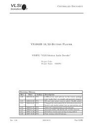
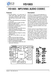
<strong>VS1003</strong><br />
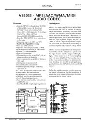
<strong>VS1003</strong> - MP3/WMA AUDIO CODEC<br />
Features<br />
• Decodes MPEG 1 & 2 audio layer III<br />
(CBR +VBR +ABR); WMA 4.0/4.1/7/8/9<br />
all profiles (5-384kbit/s); WAV (PCM +<br />
IMA ADPCM); General MIDI / SP-MIDI<br />
files<br />
• Encodes IMA ADPCM from microphone<br />
or line input<br />
• Streaming support for MP3 and WAV<br />
• Bass and treble controls<br />
• Operates with a single 12..13 MHz clock<br />
• Internal PLL clock multiplier<br />
• Low-power operation<br />
• High-quality on-chip stereo DAC with no<br />
phase error between channels<br />
• Stereo earphone driver capable of driving<br />
a 30Ω load<br />
• Separate operating voltages for analog,<br />
digital and I/O<br />
• 5.5 KiB On-chip RAM for user code /<br />
data<br />
• Serial control and data interfaces<br />
• Can be used as a slave co-processor<br />
• SPI flash boot for special applications<br />
• UART for debugging purposes<br />
• New functions may be added with software<br />
and 4 GPIO pins<br />
mic<br />
audio<br />
line<br />
audio<br />
GPIO<br />
DREQ<br />
SO<br />
SI<br />
SCLK<br />
XCS<br />
XDCS<br />
RX<br />
TX<br />
<strong>VS1003</strong><br />
MIC AMP<br />
4<br />
Serial<br />
Data/<br />
Control<br />
Interface<br />
UART<br />
Clock<br />
multiplier<br />
MUX<br />
GPIO<br />
Instruction<br />
RAM<br />
Mono<br />
ADC<br />
VSDSP 4<br />
Stereo<br />
DAC<br />
Instruction<br />
ROM<br />
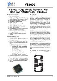
Description<br />
<strong>VS1003</strong> is a single-chip MP3/WMA/MIDI audio<br />
decoder and ADPCM encoder. It contains<br />
a high-performance, proprietary low-power DSP<br />
processor core VS_DSP 4 , working data memory,<br />
5 KiB instruction RAM and 0.5 KiB data<br />
RAM for user applications, serial control and<br />
input data interfaces, 4 general purpose I/O<br />
pins, an UART, as well as a high-quality variablesample-rate<br />
mono ADC and stereo DAC, followed<br />
by an earphone amplifier and a common<br />
buffer.<br />
<strong>VS1003</strong> receives its input bitstream through<br />
a serial input bus, which it listens to as a<br />
system slave. The input stream is decoded<br />
and passed through a digital volume control<br />
to an 18-bit oversampling, multi-bit, sigmadelta<br />
DAC. The decoding is controlled via a<br />
serial control bus. In addition to the basic decoding,<br />
it is possible to add application specific<br />
features, like DSP effects, to the user<br />
RAM memory.<br />
Stereo Ear−<br />
phone Driver<br />
Version: 1.06, 2012-03-16 1<br />
X ROM<br />
X RAM<br />
Y ROM<br />
Y RAM<br />
audio<br />
L<br />
R<br />
output
Contents<br />
<strong>VS1003</strong><br />
CONTENTS<br />
<strong>VS1003</strong> 1<br />
Table of Contents 2<br />
List of Figures 5<br />
1 Licenses 6<br />
2 Disclaimer 6<br />
3 Definitions 6<br />
4 Characteristics & Specifications 7<br />
4.1 Absolute Maximum Ratings . . . . . . . . . . . . . . . . . . . . . . . . . . . . . 7<br />
4.2 Recommended Operating Conditions . . . . . . . . . . . . . . . . . . . . . . . . 7<br />
4.3 Analog Characteristics . . . . . . . . . . . . . . . . . . . . . . . . . . . . . . . . 8<br />
4.4 Power Consumption . . . . . . . . . . . . . . . . . . . . . . . . . . . . . . . . . 9<br />
4.5 Digital Characteristics . . . . . . . . . . . . . . . . . . . . . . . . . . . . . . . . . 9<br />
4.6 Switching Characteristics - Boot Initialization . . . . . . . . . . . . . . . . . . . . 9<br />
4.7 Typical characteristics . . . . . . . . . . . . . . . . . . . . . . . . . . . . . . . . 10<br />
4.7.1 Line input ADC . . . . . . . . . . . . . . . . . . . . . . . . . . . . . . 10<br />
4.7.2 Microphone input ADC . . . . . . . . . . . . . . . . . . . . . . . . . . 10<br />
4.7.3 RIGHT and LEFT outputs . . . . . . . . . . . . . . . . . . . . . . . . 11<br />
5 Packages and Pin Descriptions 12<br />
5.1 Packages . . . . . . . . . . . . . . . . . . . . . . . . . . . . . . . . . . . . . . . 12<br />
5.1.1 LQFP-48 . . . . . . . . . . . . . . . . . . . . . . . . . . . . . . . . . . 12<br />
5.1.2 BGA-49 . . . . . . . . . . . . . . . . . . . . . . . . . . . . . . . . . . 12<br />
5.2 LQFP-48 and BGA-49 Pin Descriptions . . . . . . . . . . . . . . . . . . . . . . . 13<br />
6 Connection Diagram, LQFP-48 15<br />
7 SPI Buses 16<br />
7.1 General . . . . . . . . . . . . . . . . . . . . . . . . . . . . . . . . . . . . . . . . 16<br />
7.2 SPI Bus Pin Descriptions . . . . . . . . . . . . . . . . . . . . . . . . . . . . . . . 16<br />
7.2.1 VS1002 Native Modes (New Mode) . . . . . . . . . . . . . . . . . . . 16<br />
7.2.2 VS1001 Compatibility Mode . . . . . . . . . . . . . . . . . . . . . . . 16<br />
7.3 Data Request Pin DREQ . . . . . . . . . . . . . . . . . . . . . . . . . . . . . . . 17<br />
7.4 Serial Protocol for Serial Data Interface (SDI) . . . . . . . . . . . . . . . . . . . 17<br />
7.4.1 General . . . . . . . . . . . . . . . . . . . . . . . . . . . . . . . . . . 17<br />
7.4.2 SDI in VS1002 Native Modes (New Mode) . . . . . . . . . . . . . . . 17<br />
7.4.3 SDI in VS1001 Compatibility Mode . . . . . . . . . . . . . . . . . . . 18<br />
7.4.4 Passive SDI Mode . . . . . . . . . . . . . . . . . . . . . . . . . . . . 18<br />
7.5 Serial Protocol for Serial Command Interface (SCI) . . . . . . . . . . . . . . . . 18<br />
7.5.1 General . . . . . . . . . . . . . . . . . . . . . . . . . . . . . . . . . . 18<br />
7.5.2 SCI Read . . . . . . . . . . . . . . . . . . . . . . . . . . . . . . . . . 19<br />
7.5.3 SCI Write . . . . . . . . . . . . . . . . . . . . . . . . . . . . . . . . . 19<br />
7.6 SPI Timing Diagram . . . . . . . . . . . . . . . . . . . . . . . . . . . . . . . . . 20<br />
7.7 SPI Examples with SM_SDINEW and SM_SDISHARED set . . . . . . . . . . . 21<br />
7.7.1 Two SCI Writes . . . . . . . . . . . . . . . . . . . . . . . . . . . . . . 21<br />
Version: 1.06, 2012-03-16 2
<strong>VS1003</strong><br />
CONTENTS<br />
7.7.2 Two SDI Bytes . . . . . . . . . . . . . . . . . . . . . . . . . . . . . . . 21<br />
7.7.3 SCI Operation in Middle of Two SDI Bytes . . . . . . . . . . . . . . . 22<br />
8 Functional Description 23<br />
8.1 Main Features . . . . . . . . . . . . . . . . . . . . . . . . . . . . . . . . . . . . . 23<br />
8.2 Supported Audio Codecs . . . . . . . . . . . . . . . . . . . . . . . . . . . . . . . 23<br />
8.2.1 Supported MP3 (MPEG layer III) Formats . . . . . . . . . . . . . . . 23<br />
8.2.2 Supported WMA Formats . . . . . . . . . . . . . . . . . . . . . . . . 24<br />
8.2.3 Supported RIFF WAV Formats . . . . . . . . . . . . . . . . . . . . . . 25<br />
8.2.4 Supported MIDI Formats . . . . . . . . . . . . . . . . . . . . . . . . . 26<br />
8.3 Data Flow of <strong>VS1003</strong> . . . . . . . . . . . . . . . . . . . . . . . . . . . . . . . . . 27<br />
8.4 Serial Data Interface (SDI) . . . . . . . . . . . . . . . . . . . . . . . . . . . . . . 27<br />
8.5 Serial Control Interface (SCI) . . . . . . . . . . . . . . . . . . . . . . . . . . . . 28<br />
8.6 SCI Registers . . . . . . . . . . . . . . . . . . . . . . . . . . . . . . . . . . . . . 28<br />
8.6.1 SCI_MODE (RW) . . . . . . . . . . . . . . . . . . . . . . . . . . . . . 29<br />
8.6.2 SCI_STATUS (RW) . . . . . . . . . . . . . . . . . . . . . . . . . . . . 31<br />
8.6.3 SCI_BASS (RW) . . . . . . . . . . . . . . . . . . . . . . . . . . . . . 31<br />
8.6.4 SCI_CLOCKF (RW) . . . . . . . . . . . . . . . . . . . . . . . . . . . . 32<br />
8.6.5 SCI_DECODE_TIME (RW) . . . . . . . . . . . . . . . . . . . . . . . 33<br />
8.6.6 SCI_AUDATA (RW) . . . . . . . . . . . . . . . . . . . . . . . . . . . . 33<br />
8.6.7 SCI_WRAM (RW) . . . . . . . . . . . . . . . . . . . . . . . . . . . . . 33<br />
8.6.8 SCI_WRAMADDR (W) . . . . . . . . . . . . . . . . . . . . . . . . . . 33<br />
8.6.9 SCI_HDAT0 and SCI_HDAT1 (R) . . . . . . . . . . . . . . . . . . . . 34<br />
8.6.10 SCI_AIADDR (RW) . . . . . . . . . . . . . . . . . . . . . . . . . . . . 35<br />
8.6.11 SCI_VOL (RW) . . . . . . . . . . . . . . . . . . . . . . . . . . . . . . 36<br />
8.6.12 SCI_AICTRL[x] (RW) . . . . . . . . . . . . . . . . . . . . . . . . . . . 36<br />
9 Operation 37<br />
9.1 Clocking . . . . . . . . . . . . . . . . . . . . . . . . . . . . . . . . . . . . . . . . 37<br />
9.2 Hardware Reset . . . . . . . . . . . . . . . . . . . . . . . . . . . . . . . . . . . . 37<br />
9.3 Software Reset . . . . . . . . . . . . . . . . . . . . . . . . . . . . . . . . . . . . 37<br />
9.4 ADPCM Recording . . . . . . . . . . . . . . . . . . . . . . . . . . . . . . . . . . 38<br />
9.4.1 Activating ADPCM mode . . . . . . . . . . . . . . . . . . . . . . . . . 38<br />
9.4.2 Reading IMA ADPCM Data . . . . . . . . . . . . . . . . . . . . . . . 38<br />
9.4.3 Adding a RIFF Header . . . . . . . . . . . . . . . . . . . . . . . . . . 39<br />
9.4.4 Playing ADPCM Data . . . . . . . . . . . . . . . . . . . . . . . . . . . 40<br />
9.4.5 Sample Rate Considerations . . . . . . . . . . . . . . . . . . . . . . . 40<br />
9.4.6 Example Code . . . . . . . . . . . . . . . . . . . . . . . . . . . . . . . 40<br />
9.5 SPI Boot . . . . . . . . . . . . . . . . . . . . . . . . . . . . . . . . . . . . . . . . 42<br />
9.6 Play/Decode . . . . . . . . . . . . . . . . . . . . . . . . . . . . . . . . . . . . . . 42<br />
9.7 Feeding PCM data . . . . . . . . . . . . . . . . . . . . . . . . . . . . . . . . . . 42<br />
9.8 SDI Tests . . . . . . . . . . . . . . . . . . . . . . . . . . . . . . . . . . . . . . . 43<br />
9.8.1 Sine Test . . . . . . . . . . . . . . . . . . . . . . . . . . . . . . . . . . 43<br />
9.8.2 Pin Test . . . . . . . . . . . . . . . . . . . . . . . . . . . . . . . . . . 44<br />
9.8.3 Memory Test . . . . . . . . . . . . . . . . . . . . . . . . . . . . . . . . 44<br />
9.8.4 SCI Test . . . . . . . . . . . . . . . . . . . . . . . . . . . . . . . . . . 44<br />
10 <strong>VS1003</strong> Registers 45<br />
10.1 Who Needs to Read This Chapter . . . . . . . . . . . . . . . . . . . . . . . . . . 45<br />
10.2 The Processor Core . . . . . . . . . . . . . . . . . . . . . . . . . . . . . . . . . 45<br />
10.3 <strong>VS1003</strong> Memory Map . . . . . . . . . . . . . . . . . . . . . . . . . . . . . . . . . 45<br />
Version: 1.06, 2012-03-16 3
<strong>VS1003</strong><br />
CONTENTS<br />
10.4 SCI Registers . . . . . . . . . . . . . . . . . . . . . . . . . . . . . . . . . . . . . 45<br />
10.5 Serial Data Registers . . . . . . . . . . . . . . . . . . . . . . . . . . . . . . . . . 46<br />
10.6 DAC Registers . . . . . . . . . . . . . . . . . . . . . . . . . . . . . . . . . . . . . 47<br />
10.7 GPIO Registers . . . . . . . . . . . . . . . . . . . . . . . . . . . . . . . . . . . . 47<br />
10.8 Interrupt Registers . . . . . . . . . . . . . . . . . . . . . . . . . . . . . . . . . . 48<br />
10.9 A/D Modulator Registers . . . . . . . . . . . . . . . . . . . . . . . . . . . . . . . 49<br />
10.10 Watchdog v1.0 2002-08-26 . . . . . . . . . . . . . . . . . . . . . . . . . . . . . . 50<br />
10.10.1 Registers . . . . . . . . . . . . . . . . . . . . . . . . . . . . . . . . . . 50<br />
10.11 UART v1.0 2002-04-23 . . . . . . . . . . . . . . . . . . . . . . . . . . . . . . . . . 51<br />
10.11.1 Registers . . . . . . . . . . . . . . . . . . . . . . . . . . . . . . . . . . 51<br />
10.11.2 Status UARTx_STATUS . . . . . . . . . . . . . . . . . . . . . . . . . 51<br />
10.11.3 Data UARTx_DATA . . . . . . . . . . . . . . . . . . . . . . . . . . . . 52<br />
10.11.4 Data High UARTx_DATAH . . . . . . . . . . . . . . . . . . . . . . . . 52<br />
10.11.5 Divider UARTx_DIV . . . . . . . . . . . . . . . . . . . . . . . . . . . . 52<br />
10.11.6 Interrupts and Operation . . . . . . . . . . . . . . . . . . . . . . . . . 53<br />
10.12 Timers v1.0 2002-04-23 . . . . . . . . . . . . . . . . . . . . . . . . . . . . . . . . 54<br />
10.12.1 Registers . . . . . . . . . . . . . . . . . . . . . . . . . . . . . . . . . . 54<br />
10.12.2 Configuration TIMER_CONFIG . . . . . . . . . . . . . . . . . . . . . 54<br />
10.12.3 Configuration TIMER_ENABLE . . . . . . . . . . . . . . . . . . . . . 55<br />
10.12.4 Timer X Startvalue TIMER_Tx[L/H] . . . . . . . . . . . . . . . . . . . 55<br />
10.12.5 Timer X Counter TIMER_TxCNT[L/H] . . . . . . . . . . . . . . . . . . 55<br />
10.12.6 Interrupts . . . . . . . . . . . . . . . . . . . . . . . . . . . . . . . . . 55<br />
10.13 System Vector Tags . . . . . . . . . . . . . . . . . . . . . . . . . . . . . . . . . . 56<br />
10.13.1 AudioInt, 0x20 . . . . . . . . . . . . . . . . . . . . . . . . . . . . . . . 56<br />
10.13.2 SciInt, 0x21 . . . . . . . . . . . . . . . . . . . . . . . . . . . . . . . . 56<br />
10.13.3 DataInt, 0x22 . . . . . . . . . . . . . . . . . . . . . . . . . . . . . . . 56<br />
10.13.4 ModuInt, 0x23 . . . . . . . . . . . . . . . . . . . . . . . . . . . . . . . 56<br />
10.13.5 TxInt, 0x24 . . . . . . . . . . . . . . . . . . . . . . . . . . . . . . . . . 57<br />
10.13.6 RxInt, 0x25 . . . . . . . . . . . . . . . . . . . . . . . . . . . . . . . . 57<br />
10.13.7 Timer0Int, 0x26 . . . . . . . . . . . . . . . . . . . . . . . . . . . . . . 57<br />
10.13.8 Timer1Int, 0x27 . . . . . . . . . . . . . . . . . . . . . . . . . . . . . . 57<br />
10.13.9 UserCodec, 0x0 . . . . . . . . . . . . . . . . . . . . . . . . . . . . . . 58<br />
10.14 System Vector Functions . . . . . . . . . . . . . . . . . . . . . . . . . . . . . . . 58<br />
10.14.1 WriteIRam(), 0x2 . . . . . . . . . . . . . . . . . . . . . . . . . . . . . 58<br />
10.14.2 ReadIRam(), 0x4 . . . . . . . . . . . . . . . . . . . . . . . . . . . . . 58<br />
10.14.3 DataBytes(), 0x6 . . . . . . . . . . . . . . . . . . . . . . . . . . . . . 59<br />
10.14.4 GetDataByte(), 0x8 . . . . . . . . . . . . . . . . . . . . . . . . . . . . 59<br />
10.14.5 GetDataWords(), 0xa . . . . . . . . . . . . . . . . . . . . . . . . . . . 59<br />
10.14.6 Reboot(), 0xc . . . . . . . . . . . . . . . . . . . . . . . . . . . . . . . 59<br />
11 Document Version Changes 60<br />
12 Contact Information 61<br />
Version: 1.06, 2012-03-16 4
List of Figures<br />
<strong>VS1003</strong><br />
LIST OF FIGURES<br />
1 Measured ADC performance of the LINEIN pin. . . . . . . . . . . . . . . . . . . . 10<br />
2 Measured ADC performance of the MIC pins (differential). . . . . . . . . . . . . . 10<br />
3 Measured performance of RIGHT (or LEFT) output. . . . . . . . . . . . . . . . . 11<br />
4 Typical spectrum of RIGHT (or LEFT) output. . . . . . . . . . . . . . . . . . . . . 11<br />
5 Pin Configuration, LQFP-48. . . . . . . . . . . . . . . . . . . . . . . . . . . . . . 12<br />
6 Pin Configuration, BGA-49. . . . . . . . . . . . . . . . . . . . . . . . . . . . . . . 12<br />
7 Typical Connection Diagram Using LQFP-48. . . . . . . . . . . . . . . . . . . . . 15<br />
8 BSYNC Signal - one byte transfer. . . . . . . . . . . . . . . . . . . . . . . . . . . 18<br />
9 BSYNC Signal - two byte transfer. . . . . . . . . . . . . . . . . . . . . . . . . . . 18<br />
10 SCI Word Read . . . . . . . . . . . . . . . . . . . . . . . . . . . . . . . . . . . . . 19<br />
11 SCI Word Write . . . . . . . . . . . . . . . . . . . . . . . . . . . . . . . . . . . . . 19<br />
12 SPI Timing Diagram. . . . . . . . . . . . . . . . . . . . . . . . . . . . . . . . . . . 20<br />
13 Two SCI Operations. . . . . . . . . . . . . . . . . . . . . . . . . . . . . . . . . . . 21<br />
14 Two SDI Bytes. . . . . . . . . . . . . . . . . . . . . . . . . . . . . . . . . . . . . . 21<br />
15 Two SDI Bytes Separated By an SCI Operation. . . . . . . . . . . . . . . . . . . . 22<br />
16 Data Flow of <strong>VS1003</strong>. . . . . . . . . . . . . . . . . . . . . . . . . . . . . . . . . . 27<br />
17 ADPCM Frequency Responses with 8kHz sample rate. . . . . . . . . . . . . . . 30<br />
18 User’s Memory Map. . . . . . . . . . . . . . . . . . . . . . . . . . . . . . . . . . . 46<br />
19 RS232 Serial Interface Protocol . . . . . . . . . . . . . . . . . . . . . . . . . . . . 51<br />
Version: 1.06, 2012-03-16 5
1 Licenses<br />
<strong>VS1003</strong><br />
MPEG Layer-3 audio decoding technology licensed from Fraunhofer IIS and Thomson.<br />
3 DEFINITIONS<br />
<strong>VS1003</strong> contains WMA decoding technology from Microsoft.<br />
This product is protected by certain intellectual property rights of Microsoft and cannot<br />
be used or further distributed without a license from Microsoft.<br />
2 Disclaimer<br />
All properties and figures are subject to change.<br />
3 Definitions<br />
B Byte, 8 bits.<br />
b Bit.<br />
Ki “Kibi” = 2 10 = 1024 (IEC 60027-2).<br />
Mi “Mebi” = 2 20 = 1048576 (IEC 60027-2).<br />
VS_DSP <strong>VLSI</strong> <strong>Solution</strong>’s DSP core.<br />
W Word. In VS_DSP, instruction words are 32-bit and data words are 16-bit wide.<br />
Version: 1.06, 2012-03-16 6
4 Characteristics & Specifications<br />
4.1 Absolute Maximum Ratings<br />
<strong>VS1003</strong><br />
4 CHARACTERISTICS & SPECIFICATIONS<br />
Parameter Symbol Min Max Unit<br />
Analog Positive Supply AVDD -0.3 2.85 V<br />
Digital Positive Supply: <strong>VS1003</strong>B-L / <strong>VS1003</strong>B-B CVDD -0.3 2.85 V<br />
Digital Positive Supply: <strong>VS1003</strong>B-LK CVDD -0.3 2.7 V<br />
I/O Positive Supply IOVDD -0.3 3.6 V<br />
Current at Any Digital Output ±50 mA<br />
Voltage at Any Digital Input -0.3 IOVDD+0.3 1 V<br />
Operating Temperature -40 +85 ◦ C<br />
Storage Temperature -65 +150 ◦ C<br />
1 Must not exceed 3.6 V<br />
4.2 Recommended Operating Conditions<br />
Parameter Symbol Min Typ Max Unit<br />
Ambient Operating Temperature -40 +85 ◦ C<br />
Analog and Digital Ground 1 AGND DGND 0.0 V<br />
Positive Analog AVDD 2.6 2.8 2.85 V<br />
Positive Digital: <strong>VS1003</strong>B-L / <strong>VS1003</strong>B-B CVDD 2.4 2.5 2.85 V<br />
Positive Digital: <strong>VS1003</strong>B-LK CVDD 2.4 2.5 2.7 V<br />
I/O Voltage IOVDD CVDD-0.6V 2.8 3.6 V<br />
Input Clock Frequency 2 XTALI 12 12.288 13 MHz<br />
Internal Clock Frequency CLKI 12 36.864 52.0 4 MHz<br />
Internal Clock Multiplier 3 1.0× 3.0× 4.5× 4<br />
Master Clock Duty Cycle 40 50 60 %<br />
1 Must be connected together as close the device as possible for latch-up immunity.<br />
2 The maximum sample rate that can be played with correct speed is XTALI/256.<br />
Thus, XTALI must be at least 12.288 MHz to be able to play 48 kHz at correct speed.<br />
3 Reset value is 1.0×. Recommended SC_MULT=3.0×, SC_ADD=1.0× (SCI_CLOCKF=0x9000).<br />
4 52.0 MHz is the maximum clock for the full CVDD range.<br />
(4.0 × 12.288 MHz=49.152 MHz or 4.0 × 13.0 MHz=52.0 MHz)<br />
Version: 1.06, 2012-03-16 7
4.3 Analog Characteristics<br />
<strong>VS1003</strong><br />
4 CHARACTERISTICS & SPECIFICATIONS<br />
Unless otherwise noted: AVDD=2.85V, CVDD=2.5V, IOVDD=-2.8V, TA=-25..+70 ◦ C,<br />
XTALI=12.288MHz, DAC tested with 1307.894 Hz full-scale output sinewave, measurement<br />
bandwidth 20..20000 Hz, analog output load: LEFT to GBUF 30Ω, RIGHT to GBUF 30Ω. Microphone<br />
test amplitude 50 mVpp, f=1 kHz, Line input test amplitude 2.2 Vpp, f=1 kHz.<br />
Parameter Symbol Min Typ Max Unit<br />
DAC Resolution 18 bits<br />
Total Harmonic Distortion THD 0.1 0.3 %<br />
Dynamic Range (DAC unmuted, A-weighted) IDR >90 dB<br />
S/N Ratio (full scale signal) SNR 70 5 83 4 dB<br />
Interchannel Isolation (Cross Talk) 50 75 dB<br />
Interchannel Isolation (Cross Talk), with GBUF 40 dB<br />
Interchannel Gain Mismatch -0.5 ±0.2 0.5 dB<br />
Frequency Response -0.1 0.1 dB<br />
Full Scale Output Voltage (Peak-to-peak) 1.3 1.5 1 1.7 Vpp<br />
Deviation from Linear Phase 5 ◦<br />
Analog Output Load Resistance AOLR 16 30 2 Ω<br />
Analog Output Load Capacitance 100 pF<br />
Microphone input amplifier gain MICG 26 dB<br />
Microphone input amplitude 50 140 3 mVpp AC<br />
Microphone Total Harmonic Distortion MTHD 0.02 0.10 %<br />
Microphone S/N Ratio MSNR 50 5 68 dB<br />
Line input amplitude 2200 2800 3 mVpp AC<br />
Line input Total Harmonic Distortion LTHD 0.015 0.10 %<br />
Line input S/N Ratio LSNR 60 5 86 dB<br />
Line and Microphone input impedances 100 kΩ<br />
Typical values are measured of about 5000 devices of Lot 4234011, Week Code 0452.<br />
1 3.0 volts can be achieved with +-to-+ wiring for mono difference sound.<br />
2 AOLR may be much lower, but below Typical distortion performance may be compromised.<br />
3 Above typical amplitude the Harmonic Distortion increases.<br />
4 Unweighted, A-weighted is about 3 dB better.<br />
5 Limit low due to noise level of production tester.<br />
Version: 1.06, 2012-03-16 8
4.4 Power Consumption<br />
<strong>VS1003</strong><br />
4 CHARACTERISTICS & SPECIFICATIONS<br />
Tested with an MPEG 1.0 Layer-3 128 kbit/s sample and generated sine. Output at full volume.<br />
XTALI 12.288 MHz. Internal clock multiplier 3.0×. CVDD = 2.5 V, AVDD = 2.8 V.<br />
Parameter Min Typ Max Unit<br />
Power Supply Consumption AVDD, Reset 0.6 5.0 µA<br />
Power Supply Consumption CVDD, Reset, +25 ◦ C 3.7 40.0 µA<br />
Power Supply Consumption CVDD, Reset, +85 ◦ C 200.0 µA<br />
Power Supply Consumption AVDD, sine test, 30Ω + GBUF 36.9 mA<br />
Power Supply Consumption CVDD, sine test 12.4 mA<br />
Power Supply Consumption AVDD, no load 7.0 mA<br />
Power Supply Consumption AVDD, output load 30Ω 10.9 mA<br />
Power Supply Consumption AVDD, 30Ω + GBUF 16.1 mA<br />
Power Supply Consumption CVDD 17.5 mA<br />
4.5 Digital Characteristics<br />
Parameter Symbol Min Typ Max Unit<br />
High-Level Input Voltage 0.7×IOVDD IOVDD+0.3 1 V<br />
Low-Level Input Voltage -0.2 0.3×IOVDD V<br />
High-Level Output Voltage at IO = -1.0 mA 0.7×IOVDD V<br />
Low-Level Output Voltage at IO = 1.0 mA 0.3×IOVDD V<br />
Input Leakage Current -1.0 1.0 µA<br />
SPI Input Clock Frequency 2<br />
Rise time of all output pins, load = 50 pF<br />
CLKI<br />
7<br />
50<br />
MHz<br />
ns<br />
1 Must not exceed 3.6V<br />
2 Value for SCI reads. SCI and SDI writes allow CLKI<br />
4 .<br />
4.6 Switching Characteristics - Boot Initialization<br />
Parameter Symbol Min Max Unit<br />
XRESET active time 2 XTALI<br />
XRESET inactive to software ready 16600 50000 1 XTALI<br />
Power on reset, rise time to CVDD 10 V/s<br />
1 DREQ rises when initialization is complete. You should not send any data or commands<br />
before that.<br />
Version: 1.06, 2012-03-16 9
4.7 Typical characteristics<br />
4.7.1 Line input ADC<br />
dB<br />
100<br />
90<br />
80<br />
70<br />
60<br />
50<br />
40<br />
<strong>VS1003</strong><br />
4 CHARACTERISTICS & SPECIFICATIONS<br />
30<br />
SNR<br />
SNRa<br />
20<br />
THD<br />
0.001 0.01 0.1 1<br />
input voltage (rms)<br />
Figure 1: Measured ADC performance of the LINEIN pin.<br />
Measured ADC performance of the LINEIN pin. X-axis is rms amplitude of 1 kHz sine input.<br />
Curves are unweighted signal-to-noise ratio (blue), A-weighted signal-to-noise ratio (green),<br />
and unweighted signal-to-distortion ratio (red). Sampling rate of ADC is 48 kHz (master clock<br />
12.288 MHz), noise calculated from 0 to 20 kHz.<br />
4.7.2 Microphone input ADC<br />
dB<br />
100<br />
90<br />
80<br />
70<br />
60<br />
50<br />
40<br />
30<br />
SNR<br />
SNRa<br />
20<br />
THD<br />
0.001 0.01 0.1<br />
input voltage (rms)<br />
Figure 2: Measured ADC performance of the MIC pins (differential).<br />
Measured ADC performance of the MIC pins (differential). Other settings same as in Fig. 1.<br />
Version: 1.06, 2012-03-16 10
4.7.3 RIGHT and LEFT outputs<br />
dB<br />
100<br />
80<br />
60<br />
40<br />
<strong>VS1003</strong><br />
4 CHARACTERISTICS & SPECIFICATIONS<br />
20<br />
SNR 30R LOAD<br />
SNR AWEIGHT 30R LOAD<br />
THD 30R LOAD<br />
0<br />
THD NO LOAD<br />
0.001 0.01 0.1 1<br />
output voltage (rms)<br />
Figure 3: Measured performance of RIGHT (or LEFT) output.<br />
Measured performance of RIGHT (or LEFT) output with 1 kHz generated sine. Sampling rate<br />
of DAC is 48 kHz (master clock 12.288 MHz), noise calculated from 0 to 20 kHz.<br />
amplitude dB<br />
0<br />
-20<br />
-40<br />
-60<br />
-80<br />
-100<br />
-120<br />
0 5000 10000 15000 20000<br />
frequency Hz<br />
Figure 4: Typical spectrum of RIGHT (or LEFT) output.<br />
Typical spectrum of RIGHT (or LEFT) output with maximum level and 30 Ohm load. Setup is<br />
the same is in Fig. 3.<br />
Version: 1.06, 2012-03-16 11
5 Packages and Pin Descriptions<br />
5.1 Packages<br />
<strong>VS1003</strong> 5 PACKAGES AND PIN DESCRIPTIONS<br />
Both LPQFP-48 and BGA-49 are lead (Pb) free and also RoHS compliant packages. RoHS<br />
is a short name of Directive 2002/95/EC on the restriction of the use of certain hazardous<br />
substances in electrical and electronic equipment.<br />
5.1.1 LQFP-48<br />
1<br />
48<br />
Figure 5: Pin Configuration, LQFP-48.<br />
LQFP-48 package dimensions are at http://www.vlsi.fi/ .<br />
5.1.2 BGA-49<br />
1.10 REF<br />
A<br />
B<br />
C<br />
D<br />
E<br />
F<br />
G<br />
A1 BALL PAD CORNER<br />
1 2 3 4 5 6 7<br />
0.80 TYP<br />
4.80<br />
7.00<br />
TOP VIEW<br />
Figure 6: Pin Configuration, BGA-49.<br />
BGA-49 package dimensions are at http://www.vlsi.fi/ .<br />
Version: 1.06, 2012-03-16 12<br />
1.10 REF<br />
0.80 TYP<br />
4.80<br />
7.00
5.2 LQFP-48 and BGA-49 Pin Descriptions<br />
Pin Name LQFP-<br />
48<br />
Pin<br />
BGA49<br />
Ball<br />
Pin<br />
Type<br />
<strong>VS1003</strong> 5 PACKAGES AND PIN DESCRIPTIONS<br />
Function<br />
MICP 1 C3 AI Positive differential microphone input, self-biasing<br />
MICN 2 C2 AI Negative differential microphone input, self-biasing<br />
XRESET 3 B1 DI Active low asynchronous reset<br />
DGND0 4 D2 DGND Core & I/O ground<br />
CVDD0 5 C1 CPWR Core power supply<br />
IOVDD0 6 D3 IOPWR I/O power supply<br />
CVDD1 7 D1 CPWR Core power supply<br />
DREQ 8 E2 DO Data request, input bus<br />
GPIO2 / DCLK 1 9 E1 DIO General purpose IO 2 / serial input data bus clock<br />
GPIO3 / SDATA 1 10 F2 DIO General purpose IO 3 / serial data input<br />
XDCS / BSYNC 1 13 E3 DI Data chip select / byte sync<br />
IOVDD1 14 F3 IOPWR I/O power supply<br />
VCO 15 G2 DO For testing only (Clock VCO output)<br />
DGND1 16 F4 DGND Core & I/O ground<br />
XTALO 17 G3 AO Crystal output<br />
XTALI 18 E4 AI Crystal input<br />
IOVDD2 19 G4 IOPWR I/O power supply<br />
IOVDD3 F5 IOPWR I/O power supply<br />
DGND2 20 DGND Core & I/O ground<br />
DGND3 21 G5 DGND Core & I/O ground<br />
DGND4 22 F6 DGND Core & I/O ground<br />
XCS 23 G6 DI Chip select input (active low)<br />
CVDD2 24 G7 CPWR Core power supply<br />
RX 26 E6 DI UART receive, connect to IOVDD if not used<br />
TX 27 F7 DO UART transmit<br />
SCLK 28 D6 DI Clock for serial bus<br />
SI 29 E7 DI Serial input<br />
SO 30 D5 DO3 Serial output<br />
CVDD3 31 D7 CPWR Core power supply<br />
TEST 32 C6 DI Reserved for test, connect to IOVDD<br />
GPIO0 / SPIBOOT 33 C7 DIO General purpose IO 0 / SPIBOOT, use 100 kΩ pulldown<br />
resistor 2<br />
GPIO1 34 B6 DIO General purpose IO 1<br />
AGND0 37 C5 APWR Analog ground, low-noise reference<br />
AVDD0 38 B5 APWR Analog power supply<br />
RIGHT 39 A6 AO Right channel output<br />
AGND1 40 B4 APWR Analog ground<br />
AGND2 41 A5 APWR Analog ground<br />
GBUF 42 C4 AO Common buffer for headphones<br />
AVDD1 43 A4 APWR Analog power supply<br />
RCAP 44 B3 AIO Filtering capacitance for reference<br />
AVDD2 45 A3 APWR Analog power supply<br />
LEFT 46 B2 AO Left channel output<br />
AGND3 47 A2 APWR Analog ground<br />
LINEIN 48 A1 AI Line input<br />
1 First pin function is active in New Mode, latter in Compatibility Mode.<br />
2 Unless pull-down resistor is used, SPI Boot is tried. See Chapter 9.5 for details.<br />
Version: 1.06, 2012-03-16 13
Pin types:<br />
Type Description<br />
DI Digital input, CMOS Input Pad<br />
DO Digital output, CMOS Input Pad<br />
DIO Digital input/output<br />
DO3 Digital output, CMOS Tri-stated Output<br />
Pad<br />
AI Analog input<br />
In BGA-49, no-connect balls are A7, B7, D4, E5, F1, G1.<br />
In LQFP-48, no-connect pins are 11, 12, 25, 35, 36.<br />
<strong>VS1003</strong> 5 PACKAGES AND PIN DESCRIPTIONS<br />
Type Description<br />
AO Analog output<br />
AIO Analog input/output<br />
APWR Analog power supply pin<br />
DGND Core or I/O ground pin<br />
CPWR Core power supply pin<br />
IOPWR I/O power supply pin<br />
Version: 1.06, 2012-03-16 14
6 Connection Diagram, LQFP-48<br />
<strong>VS1003</strong> 6 CONNECTION DIAGRAM, LQFP-48<br />
Figure 7: Typical Connection Diagram Using LQFP-48.<br />
The common buffer GBUF can be used for common voltage (1.24 V) for earphones. This will<br />
eliminate the need for large isolation capacitors on line outputs, and thus the audio output pins<br />
from <strong>VS1003</strong> may be connected directly to the earphone connector.<br />
GBUF must NOT be connected to ground under any circumstances. If GBUF is not used,<br />
LEFT and RIGHT must be provided with coupling capacitors. To keep GBUF stable, you should<br />
always have the resistor and capacitor even when GBUF is not used. See application notes for<br />
details.<br />
Unused GPIO pins should have a pull-down resistor.<br />
If UART is not used, RX should be connected to IOVDD and TX be unconnected.<br />
Do not connect any external load to XTALO.<br />
Note: This connection assumes SM_SDINEW is active (see Chapter 8.6.1). If also SM_SDISHARE<br />
is used, xDCS should be tied high (see Chapter 7.2.1).<br />
Version: 1.06, 2012-03-16 15
7 SPI Buses<br />
7.1 General<br />
<strong>VS1003</strong><br />
7 SPI BUSES<br />
The SPI Bus - that was originally used in some Motorola devices - has been used for both<br />
<strong>VS1003</strong>’s Serial Data Interface SDI (Chapters 7.4 and 8.4) and Serial Control Interface SCI<br />
(Chapters 7.5 and 8.5).<br />
7.2 SPI Bus Pin Descriptions<br />
7.2.1 VS1002 Native Modes (New Mode)<br />
These modes are active on <strong>VS1003</strong> when SM_SDINEW is set to 1 (default at startup). DCLK<br />
and SDATA are not used for data transfer and they can be used as general-purpose I/O pins<br />
(GPIO2 and GPIO3). BSYNC function changes to data interface chip select (XDCS).<br />
SDI Pin SCI Pin Description<br />
XDCS XCS Active low chip select input. A high level forces the serial interface into<br />
standby mode, ending the current operation. A high level also forces serial<br />
output (SO) to high impedance state. If SM_SDISHARE is 1, pin<br />
XDCS is not used, but the signal is generated internally by inverting<br />
XCS.<br />
SCK Serial clock input. The serial clock is also used internally as the master<br />
clock for the register interface.<br />
SCK can be gated or continuous. In either case, the first rising clock edge<br />
after XCS has gone low marks the first bit to be written.<br />
SI Serial input. If a chip select is active, SI is sampled on the rising CLK edge.<br />
- SO Serial output. In reads, data is shifted out on the falling SCK edge.<br />
In writes SO is at a high impedance state.<br />
7.2.2 VS1001 Compatibility Mode<br />
This mode is active when SM_SDINEW is set to 0. In this mode, DCLK, SDATA and BSYNC<br />
are active.<br />
SDI Pin SCI Pin Description<br />
- XCS Active low chip select input. A high level forces the serial interface into<br />
standby mode, ending the current operation. A high level also forces serial<br />
output (SO) to high impedance state.<br />
BSYNC - SDI data is synchronized with a rising edge of BSYNC.<br />
DCLK SCK Serial clock input. The serial clock is also used internally as the master<br />
clock for the register interface.<br />
SCK can be gated or continuous. In either case, the first rising clock edge<br />
after XCS has gone low marks the first bit to be written.<br />
SDATA SI Serial input. SI is sampled on the rising SCK edge, if XCS is low.<br />
- SO Serial output. In reads, data is shifted out on the falling SCK edge.<br />
In writes SO is at a high impedance state.<br />
Version: 1.06, 2012-03-16 16
7.3 Data Request Pin DREQ<br />
<strong>VS1003</strong><br />
7 SPI BUSES<br />
The DREQ pin/signal is used to signal if <strong>VS1003</strong>’s FIFO is capable of receiving data. If DREQ<br />
is high, <strong>VS1003</strong> can take at least 32 bytes of SDI data or one SCI command. When these<br />
criteria are not met, DREQ is turned low, and the sender should stop transferring new data.<br />
Because of the 32-byte safety area, the sender may send upto 32 bytes of SDI data at a<br />
time without checking the status of DREQ, making controlling <strong>VS1003</strong> easier for low-speed<br />
microcontrollers.<br />
Note: DREQ may turn low or high at any time, even during a byte transmission. Thus, DREQ<br />
should only be used to decide whether to send more bytes. It should not abort a transmission<br />
that has already started.<br />
Note: In VS10XX products upto VS1002, DREQ was only used for SDI. In <strong>VS1003</strong> DREQ is<br />
also used to tell the status of SCI.<br />
There are cases when you still want to send SCI commands when DREQ is low. Because<br />
DREQ is shared between SDI and SCI, you can not determine if a SCI command has been<br />
executed if SDI is not ready to receive. In this case you need a long enough delay after every<br />
SCI command to make certain none of them is missed. The SCI Registers table in section 8.6<br />
gives the worst-case handling time for each SCI register write.<br />
7.4 Serial Protocol for Serial Data Interface (SDI)<br />
7.4.1 General<br />
The serial data interface operates in slave mode so DCLK signal must be generated by an<br />
external circuit.<br />
Data (SDATA signal) can be clocked in at either the rising or falling edge of DCLK (Chapter 8.6).<br />
<strong>VS1003</strong> assumes its data input to be byte-sychronized. SDI bytes may be transmitted either<br />
MSb or LSb first, depending of contents of SCI_MODE (Chapter 8.6.1).<br />
The firmware is able to accept the maximum bitrate the SDI supports.<br />
7.4.2 SDI in VS1002 Native Modes (New Mode)<br />
In VS1002 native modes (SM_NEWMODE is 1), byte synchronization is achieved by XDCS.<br />
The state of XDCS may not change while a data byte transfer is in progress. To always maintain<br />
data synchronization even if there may be glitches in the boards using <strong>VS1003</strong>, it is recommended<br />
to turn XDCS every now and then, for instance once after every flash data block or<br />
a few kilobytes, just to keep sure the host and <strong>VS1003</strong> are in sync.<br />
If SM_SDISHARE is 1, the XDCS signal is internally generated by inverting the XCS input.<br />
For new designs, using VS1002 native modes are recommended.<br />
Version: 1.06, 2012-03-16 17
7.4.3 SDI in VS1001 Compatibility Mode<br />
BSYNC<br />
SDATA<br />
DCLK<br />
<strong>VS1003</strong><br />
D7 D6 D5 D4 D3 D2 D1 D0<br />
Figure 8: BSYNC Signal - one byte transfer.<br />
7 SPI BUSES<br />
When <strong>VS1003</strong> is running in VS1001 compatibility mode, a BSYNC signal must be generated<br />
to ensure correct bit-alignment of the input bitstream. The first DCLK sampling edge (rising or<br />
falling, depending on selected polarity), during which the BSYNC is high, marks the first bit of<br />
a byte (LSB, if LSB-first order is used, MSB, if MSB-first order is used). If BSYNC is ’1’ when<br />
the last bit is received, the receiver stays active and next 8 bits are also received.<br />
BSYNC<br />
SDATA<br />
DCLK<br />
7.4.4 Passive SDI Mode<br />
D7 D6 D5 D4 D3 D2 D1 D0 D7 D6 D5 D4 D3 D2 D1 D0<br />
Figure 9: BSYNC Signal - two byte transfer.<br />
If SM_NEWMODE is 0 and SM_SDISHARE is 1, the operation is otherwise like the VS1001<br />
compatibility mode, but bits are only received while the BSYNC signal is ’1’. Rising edge of<br />
BSYNC is still used for synchronization.<br />
7.5 Serial Protocol for Serial Command Interface (SCI)<br />
7.5.1 General<br />
The serial bus protocol for the Serial Command Interface SCI (Chapter 8.5) consists of an<br />
instruction byte, address byte and one 16-bit data word. Each read or write operation can read<br />
or write a single register. Data bits are read at the rising edge, so the user should update data<br />
at the falling edge. Bytes are always send MSb first. XCS should be low for the full duration of<br />
the operation, but you can have pauses between bits if needed.<br />
The operation is specified by an 8-bit instruction opcode. The supported instructions are read<br />
and write. See table below.<br />
Instruction<br />
Name Opcode Operation<br />
READ 0b0000 0011 Read data<br />
WRITE 0b0000 0010 Write data<br />
Note: <strong>VS1003</strong> sets DREQ low after each SCI operation. The duration depends on the operation.<br />
It is not allowed to start a new SCI/SDI operation before DREQ is high again.<br />
Version: 1.06, 2012-03-16 18
7.5.2 SCI Read<br />
XCS<br />
SCK<br />
SI<br />
SO<br />
DREQ<br />
<strong>VS1003</strong><br />
0 1 2 3 4 5 6 7 8 9 10 11 12 13 14 15 16 17<br />
30 31<br />
0 0 0 0 0 0 1 1 0 0 0 0<br />
instruction (read) address<br />
3 2 1 0<br />
0 0 0 0 0 0 0 0 0 0 0 0 0 0 0 0<br />
Figure 10: SCI Word Read<br />
don’t care don’t care<br />
data out<br />
15 14 1 0<br />
X<br />
execution<br />
7 SPI BUSES<br />
<strong>VS1003</strong> registers are read from using the following sequence, as shown in Figure 10. First,<br />
XCS line is pulled low to select the device. Then the READ opcode (0x3) is transmitted via<br />
the SI line followed by an 8-bit word address. After the address has been read in, any further<br />
data on SI is ignored by the chip. The 16-bit data corresponding to the received address will be<br />
shifted out onto the SO line.<br />
XCS should be driven high after data has been shifted out.<br />
DREQ is driven low for a short while when in a read operation by the chip. This is a very short<br />
time and doesn’t require special user attention.<br />
7.5.3 SCI Write<br />
XCS<br />
SCK<br />
SI<br />
0 1 2 3 4 5 6 7 8 9 10 11 12 13 14 15 16 17<br />
30 31<br />
3 2 1 0 15 14<br />
1 0<br />
0 0 0 0 0 0 1 0 0 0 0 0<br />
address<br />
data out<br />
SO 0 0 0 0 0 0 0 0 0 0 0 0 0 0 0 0 0 0 0 0 X<br />
DREQ<br />
instruction (write)<br />
Figure 11: SCI Word Write<br />
X<br />
execution<br />
<strong>VS1003</strong> registers are written from using the following sequence, as shown in Figure 11. First,<br />
XCS line is pulled low to select the device. Then the WRITE opcode (0x2) is transmitted via the<br />
SI line followed by an 8-bit word address.<br />
Version: 1.06, 2012-03-16 19
<strong>VS1003</strong><br />
7 SPI BUSES<br />
After the word has been shifted in and the last clock has been sent, XCS should be pulled high<br />
to end the WRITE sequence.<br />
After the last bit has been sent, DREQ is driven low for the duration of the register update,<br />
marked “execution” in the figure. The time varies depending on the register and its contents<br />
(see table in Chapter 8.6 for details). If the maximum time is longer than what it takes from<br />
the microcontroller to feed the next SCI command or SDI byte, it is not allowed to finish a new<br />
SCI/SDI operation before DREQ has risen up again.<br />
7.6 SPI Timing Diagram<br />
XCS<br />
SCK<br />
SI<br />
SO<br />
tZ<br />
tXCSS tWL tWH<br />
tXCSH<br />
0 1 14 15 16<br />
tH<br />
tSU<br />
Figure 12: SPI Timing Diagram.<br />
Symbol Min Max Unit<br />
tV<br />
30 31<br />
tXCSS 5 ns<br />
tSU 0 ns<br />
tH 2 CLKI cycles<br />
tZ 0 ns<br />
tWL 2 CLKI cycles<br />
tWH 2 CLKI cycles<br />
tV 2 (+ 25ns 1 ) CLKI cycles<br />
tXCSH 1 CLKI<br />
tXCS 2 CLKI cycles<br />
tDIS 10 ns<br />
1 25ns is when pin loaded with 100pF capacitance. The time is shorter with lower capacitance.<br />
Note: As tWL and tWH, as well as tH require at least 2 clock cycles, the maximum speed for<br />
the SPI bus that can easily be used with asynchronous clocks is 1/7 of <strong>VS1003</strong>’s internal clock<br />
speed CLKI.<br />
Note: Although the timing is derived from the internal clock CLKI, the system always starts up<br />
in 1.0× mode, thus CLKI=XTALI.<br />
Version: 1.06, 2012-03-16 20<br />
tXCS<br />
tDIS
<strong>VS1003</strong><br />
7.7 SPI Examples with SM_SDINEW and SM_SDISHARED set<br />
7.7.1 Two SCI Writes<br />
XCS<br />
SCK<br />
SI<br />
DREQ<br />
SCI Write 1 SCI Write 2<br />
0 1 2 3 30 31<br />
32 33 61 62 63<br />
1 0 2 1 0<br />
0 0 0 0 X 0 0<br />
X<br />
Figure 13: Two SCI Operations.<br />
DREQ up before finishing next SCI write<br />
7 SPI BUSES<br />
Figure 13 shows two consecutive SCI operations. Note that xCS must be raised to inactive<br />
state between the writes. Also DREQ must be respected as shown in the figure.<br />
7.7.2 Two SDI Bytes<br />
XCS<br />
SCK<br />
SI<br />
DREQ<br />
SDI Byte 1<br />
SDI Byte 2<br />
0 1 2 3<br />
6 7 8 9 13 14 15<br />
7 6 5 4 3 1 0 7 6 5 2 1 0<br />
Figure 14: Two SDI Bytes.<br />
SDI data is synchronized with a raising edge of xCS as shown in Figure 14. However, every<br />
byte doesn’t need separate synchronization.<br />
Version: 1.06, 2012-03-16 21<br />
X
<strong>VS1003</strong><br />
7.7.3 SCI Operation in Middle of Two SDI Bytes<br />
XCS<br />
SCK<br />
SI<br />
DREQ<br />
0 1<br />
SDI Byte<br />
7 6 5 1<br />
7<br />
0 0<br />
SCI Operation<br />
SDI Byte<br />
8 9 39 40 41 46 47<br />
0 7 6 5 1 0<br />
DREQ high before end of next transfer<br />
Figure 15: Two SDI Bytes Separated By an SCI Operation.<br />
X<br />
7 SPI BUSES<br />
Figure 15 shows how an SCI operation is embedded in between SDI operations. xCS edges<br />
are used to synchronize both SDI and SCI. Remember to respect DREQ as shown in the figure.<br />
Version: 1.06, 2012-03-16 22
8 Functional Description<br />
8.1 Main Features<br />
<strong>VS1003</strong> 8 FUNCTIONAL DESCRIPTION<br />
<strong>VS1003</strong> is based on a proprietary digital signal processor, VS_DSP. It contains all the code<br />
and data memory needed for MP3, WMA and WAV PCM + ADPCM audio decoding, MIDI<br />
synthesizer, together with serial interfaces, a multirate stereo audio DAC and analog output<br />
amplifiers and filters. Also ADPCM audio encoding is supported using a microphone amplifier<br />
and A/D converter. A UART is provided for debugging purposes.<br />
8.2 Supported Audio Codecs<br />
Conventions<br />
Mark Description<br />
+ Format is supported<br />
- Format exists but is not supported<br />
Format doesn’t exist<br />
8.2.1 Supported MP3 (MPEG layer III) Formats<br />
MPEG 1.0 1 :<br />
Samplerate / Hz Bitrate / kbit/s<br />
32 40 48 56 64 80 96 112 128 160 192 224 256 320<br />
MPEG 2.0 1 :<br />
48000 + + + + + + + + + + + + + +<br />
44100 + + + + + + + + + + + + + +<br />
32000 + + + + + + + + + + + + + +<br />
Samplerate / Hz Bitrate / kbit/s<br />
8 16 24 32 40 48 56 64 80 96 112 128 144 160<br />
MPEG 2.5 1 2 :<br />
24000 + + + + + + + + + + + + + +<br />
22050 + + + + + + + + + + + + + +<br />
16000 + + + + + + + + + + + + + +<br />
Samplerate / Hz Bitrate / kbit/s<br />
8 16 24 32 40 48 56 64 80 96 112 128 144 160<br />
12000 + + + + + + + + + + + + + +<br />
11025 + + + + + + + + + + + + + +<br />
8000 + + + + + + + + + + + + + +<br />
1 Also all variable bitrate (VBR) formats are supported.<br />
2 Incompatibilities may occur because MPEG 2.5 is not a standard format.<br />
Version: 1.06, 2012-03-16 23
8.2.2 Supported WMA Formats<br />
<strong>VS1003</strong> 8 FUNCTIONAL DESCRIPTION<br />
Windows Media Audio codec versions 2, 7, 8, and 9 are supported. All WMA profiles (L1, L2,<br />
and L3) are supported. Previously streams were separated into Classes 1, 2a, 2b, and 3. WMA<br />
9 Professional and WMA 9 Lossless are not supported. The decoder has passed Microsoft’s<br />
conformance testing program.<br />
WMA 4.0 / 4.1:<br />
Samplerate Bitrate / kbit/s<br />
/ Hz 5 6 8 10 12 16 20 22 32 40 48 64 80 96 128 160 192<br />
WMA 7:<br />
8000 + + + +<br />
11025 + +<br />
16000 + + + +<br />
22050 + + + +<br />
32000 + + + + + +<br />
44100 + + + + + + +<br />
48000 + +<br />
Samplerate Bitrate / kbit/s<br />
/ Hz 5 6 8 10 12 16 20 22 32 40 48 64 80 96 128 160 192<br />
WMA 8:<br />
8000 + + + +<br />
11025 + +<br />
16000 + + + +<br />
22050 + + + +<br />
32000 + + + +<br />
44100 + + + + + + + +<br />
48000 + +<br />
Samplerate Bitrate / kbit/s<br />
/ Hz 5 6 8 10 12 16 20 22 32 40 48 64 80 96 128 160 192<br />
WMA 9:<br />
8000 + + + +<br />
11025 + +<br />
16000 + + + +<br />
22050 + + + +<br />
32000 + + + +<br />
44100 + + + + + + + +<br />
48000 + + +<br />
Samplerate Bitrate / kbit/s<br />
/ Hz 5 6 8 10 12 16 20 22 32 40 48 64 80 96 128 160 192 256 320<br />
8000 + + + +<br />
11025 + +<br />
16000 + + + +<br />
22050 + + + +<br />
32000 + + + +<br />
44100 + + + + + + + + + + +<br />
48000 + + + + +<br />
In addition to these expected WMA decoding profiles, all other bitrate and samplerate combinations<br />
are supported, including variable bitrate WMA streams. Note that WMA does not<br />
consume the bitstream as evenly as MP3, so you need a higher peak transfer capability for<br />
clean playback at the same bitrate.<br />
Version: 1.06, 2012-03-16 24
8.2.3 Supported RIFF WAV Formats<br />
The most common RIFF WAV subformats are supported.<br />
Format Name Supported Comments<br />
<strong>VS1003</strong> 8 FUNCTIONAL DESCRIPTION<br />
0x01 PCM + 16 and 8 bits, any sample rate ≤ 48kHz<br />
0x02 ADPCM -<br />
0x03 IEEE_FLOAT -<br />
0x06 ALAW -<br />
0x07 MULAW -<br />
0x10 OKI_ADPCM -<br />
0x11 IMA_ADPCM + Any sample rate ≤ 48kHz<br />
0x15 DIGISTD -<br />
0x16 DIGIFIX -<br />
0x30 DOLBY_AC2 -<br />
0x31 GSM610 -<br />
0x3b ROCKWELL_ADPCM -<br />
0x3c ROCKWELL_DIGITALK -<br />
0x40 G721_ADPCM -<br />
0x41 G728_CELP -<br />
0x50 MPEG -<br />
0x55 MPEGLAYER3 + For supported MP3 modes, see Chapter 8.2.1<br />
0x64 G726_ADPCM -<br />
0x65 G722_ADPCM -<br />
Version: 1.06, 2012-03-16 25
8.2.4 Supported MIDI Formats<br />
<strong>VS1003</strong> 8 FUNCTIONAL DESCRIPTION<br />
General MIDI and SP-MIDI format 0 files are played. Format 1 and 2 files must be converted to<br />
format 0 by the user. The maximum simultaneous polyphony is 40. Actual polyphony depends<br />
on the internal clock rate (which is user-selectable), the instruments used, and the possible<br />
postprocessing effects enabled, such as bass and treble enhancers. The polyphony restriction<br />
algorithm makes use of the SP-MIDI MIP table, if present.<br />
36.86 MHz (3.0× input clock) achieves 16-26 simultaneous sustained notes. The instantaneous<br />
amount of notes can be larger. 36 MHz is a fair compromise between power consumption and<br />
quality, but higher clocks can be used to increase polyphony.<br />
<strong>VS1003</strong>b implements 36 distinct instruments. Each melodic, effect, and percussion instrument<br />
is mapped into one of these instruments.<br />
<strong>VS1003</strong>b<br />
Melodic Effect Percussion<br />
piano reverse cymbal bass drum<br />
vibraphone guitar fret noise snare<br />
organ breath closed hihat<br />
guitar seashore open hihat<br />
distortion guitar bird tweet high tom<br />
bass telephone low tom<br />
violin helicopter crash cymbal 2<br />
strings applause ride cymbal<br />
trumpet gunshot tambourine<br />
sax high conga<br />
flute low conga<br />
lead maracas<br />
pad claves<br />
steeldrum<br />
Version: 1.06, 2012-03-16 26
8.3 Data Flow of <strong>VS1003</strong><br />
SDI<br />
Bitstream<br />
FIFO<br />
AIADDR = 0<br />
User<br />
Application<br />
AIADDR != 0<br />
MP3/PlusV/<br />
WAV/ADPCM/<br />
WMA decode/<br />
MIDI decode<br />
SM_ADPCM=0<br />
SB_AMPLITUDE=0<br />
Bass<br />
enhancer<br />
SB_AMPLITUDE!=0<br />
<strong>VS1003</strong> 8 FUNCTIONAL DESCRIPTION<br />
ST_AMPLITUDE=0<br />
Treble<br />
enhancer<br />
ST_AMPLITUDE!=0<br />
Volume<br />
control<br />
SCI_VOL<br />
Figure 16: Data Flow of <strong>VS1003</strong>.<br />
Audio<br />
FIFO<br />
2048 stereo<br />
samples<br />
S.rate.conv.<br />
and DAC<br />
First, depending on the audio data, and provided ADPCM encoding mode is not set, MP3,<br />
WMA, PCM WAV, IMA ADPCM WAV, or MIDI data is received and decoded from the SDI bus.<br />
After decoding, if SCI_AIADDR is non-zero, application code is executed from the address<br />
pointed to by that register. For more details, see Application Notes for VS10XX.<br />
Then data may be sent to the Bass and Treble Enhancer depending on the SCI_BASS register.<br />
After that the signal is fed to the volume control unit, which also copies the data to the Audio<br />
FIFO.<br />
The Audio FIFO holds the data, which is read by the Audio interrupt (Chapter 10.13.1) and fed<br />
to the sample rate converter and DACs. The size of the audio FIFO is 2048 stereo (2×16-bit)<br />
samples, or 8 KiB.<br />
The sample rate converter converts all different sample rates to XTALI/2, or 128 times the<br />
highest usable sample rate. This removes the need for complex PLL-based clocking schemes<br />
and allows almost unlimited sample rate accuracy with one fixed input clock frequency. With<br />
a 12.288 MHz clock, the DA converter operates at 128 × 48 kHz, i.e. 6.144 MHz, and creates<br />
a stereo in-phase analog signal. The oversampled output is low-pass filtered by an on-chip<br />
analog filter. This signal is then forwarded to the earphone amplifier.<br />
8.4 Serial Data Interface (SDI)<br />
The serial data interface is meant for transferring compressed MP3 or WMA data, WAV PCM<br />
and ADPCM data as well as MIDI data.<br />
If the input of the decoder is invalid or it is not received fast enough, analog outputs are automatically<br />
muted.<br />
Also several different tests may be activated through SDI as described in Chapter 9.<br />
Version: 1.06, 2012-03-16 27<br />
L<br />
R
8.5 Serial Control Interface (SCI)<br />
<strong>VS1003</strong> 8 FUNCTIONAL DESCRIPTION<br />
The serial control interface is compatible with the SPI bus specification. Data transfers are<br />
always 16 bits. <strong>VS1003</strong> is controlled by writing and reading the registers of the interface.<br />
The main controls of the control interface are:<br />
• control of the operation mode, clock, and builtin effects<br />
• access to status information and header data<br />
• access to encoded digital data<br />
• uploading user programs<br />
8.6 SCI Registers<br />
SCI registers, prefix SCI_<br />
Reg Type Reset Time 1 Abbrev[bits] Description<br />
0x0 rw 0x800 70 CLKI 4 MODE Mode control<br />
0x1 rw 0x3C 3 40 CLKI STATUS Status of <strong>VS1003</strong><br />
0x2 rw 0 2100 CLKI BASS Built-in bass/treble enhancer<br />
0x3 rw 0 11000 XTALI 5 CLOCKF Clock freq + multiplier<br />
0x4 rw 0 40 CLKI DECODE_TIME Decode time in seconds<br />
0x5 rw 0 3200 CLKI AUDATA Misc. audio data<br />
0x6 rw 0 80 CLKI WRAM RAM write/read<br />
0x7 rw 0 80 CLKI WRAMADDR Base address for RAM<br />
write/read<br />
0x8 r 0 - HDAT0 Stream header data 0<br />
0x9 r 0 - HDAT1 Stream header data 1<br />
0xA rw 0 3200 CLKI 2 AIADDR Start address of application<br />
0xB rw 0 2100 CLKI VOL Volume control<br />
0xC rw 0 50 CLKI 2 AICTRL0 Application control register 0<br />
0xD rw 0 50 CLKI 2 AICTRL1 Application control register 1<br />
0xE rw 0 50 CLKI 2 AICTRL2 Application control register 2<br />
0xF rw 0 50 CLKI 2 AICTRL3 Application control register 3<br />
1 This is the worst-case time that DREQ stays low after writing to this register. The user may<br />
choose to skip the DREQ check for those register writes that take less than 100 clock cycles to<br />
execute.<br />
2 In addition, the cycles spent in the user application routine must be counted.<br />
3 Firmware changes the value of this register immediately to 0x38, and in less than 100 ms to<br />
0x30.<br />
4 When mode register write specifies a software reset the worst-case time is 16600 XTALI<br />
cycles.<br />
5 Writing to this register may force internal clock to run at 1.0 × XTALI for a while. Thus it is not<br />
a good idea to send SCI or SDI bits while this register update is in progress.<br />
Note that if DREQ is low when an SCI write is done, DREQ also stays low after SCI write<br />
processing.<br />
Version: 1.06, 2012-03-16 28
8.6.1 SCI_MODE (RW)<br />
<strong>VS1003</strong> 8 FUNCTIONAL DESCRIPTION<br />
SCI_MODE is used to control the operation of <strong>VS1003</strong> and defaults to 0x0800 (SM_SDINEW<br />
set).<br />
Bit Name Function Value Description<br />
0 SM_DIFF Differential 0 normal in-phase audio<br />
1 left channel inverted<br />
1 SM_SETTOZERO Set to zero 0 right<br />
1 wrong<br />
2 SM_RESET Soft reset 0 no reset<br />
1 reset<br />
3 SM_OUTOFWAV Jump out of WAV decoding 0 no<br />
1 yes<br />
4 SM_PDOWN Powerdown 0 power on<br />
1 powerdown<br />
5 SM_TESTS Allow SDI tests 0 not allowed<br />
1 allowed<br />
6 SM_STREAM Stream mode 0 no<br />
1 yes<br />
7 SM_SETTOZERO2 Set to zero 0 right<br />
1 wrong<br />
8 SM_DACT DCLK active edge 0 rising<br />
1 falling<br />
9 SM_SDIORD SDI bit order 0 MSb first<br />
1 MSb last<br />
10 SM_SDISHARE Share SPI chip select 0 no<br />
1 yes<br />
11 SM_SDINEW VS1002 native SPI modes 0 no<br />
1 yes<br />
12 SM_ADPCM ADPCM recording active 0 no<br />
1 yes<br />
13 SM_ADPCM_HP ADPCM high-pass filter active 0 no<br />
1 yes<br />
14 SM_LINE_IN ADPCM recording selector 0 microphone<br />
1 line in<br />
When SM_DIFF is set, the player inverts the left channel output. For a stereo input this creates<br />
virtual surround, and for a mono input this creates a differential left/right signal.<br />
Software reset is initiated by setting SM_RESET to 1. This bit is cleared automatically.<br />
If you want to stop decoding a WAV, WMA, or MIDI file in the middle, set SM_OUTOFWAV, and<br />
send data honouring DREQ until SM_OUTOFWAV is cleared. SCI_HDAT1 will also be cleared.<br />
For WMA and MIDI it is safest to continue sending the stream, send zeroes for WAV.<br />
Bit SM_PDOWN sets <strong>VS1003</strong> into software powerdown mode. Note that software powerdown<br />
is not nearly as power efficient as hardware powerdown activated with the XRESET pin.<br />
If SM_TESTS is set, SDI tests are allowed. For more details on SDI tests, look at Chapter 9.8.<br />
Version: 1.06, 2012-03-16 29
<strong>VS1003</strong> 8 FUNCTIONAL DESCRIPTION<br />
SM_STREAM activates <strong>VS1003</strong>’s stream mode. In this mode, data should be sent with as<br />
even intervals as possible (and preferable with data blocks of less than 512 bytes), and <strong>VS1003</strong><br />
makes every attempt to keep its input buffer half full by changing its playback speed upto 5%.<br />
For best quality sound, the average speed error should be within 0.5%, the bitrate should not<br />
exceed 160 kbit/s and VBR should not be used. For details, see Application Notes for VS10XX.<br />
This mode does not work with WMA files.<br />
SM_DACT defines the active edge of data clock for SDI. When ’0’, data is read at the rising<br />
edge, when ’1’, data is read at the falling edge.<br />
When SM_SDIORD is clear, bytes on SDI are sent as a default MSb first. By setting SM_SDIORD,<br />
the user may reverse the bit order for SDI, i.e. bit 0 is received first and bit 7 last. Bytes are,<br />
however, still sent in the default order. This register bit has no effect on the SCI bus.<br />
Setting SM_SDISHARE makes SCI and SDI share the same chip select, as explained in Chapter<br />
7.2, if also SM_SDINEW is set.<br />
Setting SM_SDINEW will activate VS1002 native serial modes as described in Chapters 7.2.1 and 7.4.2.<br />
Note, that this bit is set as a default when <strong>VS1003</strong> is started up.<br />
By activating SM_ADPCM and SM_RESET at the same time, the user will activate IMA ADPCM<br />
recording mode. More information is available in the Application Notes for VS10XX.<br />
If SM_ADPCM_HP is set at the same time as SM_ADPCM and SM_RESET, ADPCM mode<br />
will start with a high-pass filter. This may help intelligibility of speech when there is lots of<br />
background noise. The difference created to the ADPCM encoder frequency response is as<br />
shown in Figure 17.<br />
Amplitude / dB<br />
5<br />
0<br />
−5<br />
−10<br />
−15<br />
<strong>VS1003</strong> AD Converter with and Without HP Filter<br />
No High−Pass<br />
High−Pass<br />
−20<br />
0 500 1000 1500 2000<br />
Frequency / Hz<br />
2500 3000 3500 4000<br />
Figure 17: ADPCM Frequency Responses with 8kHz sample rate.<br />
SM_LINE_IN is used to select the input for ADPCM recording. If ’0’, microphone input pins<br />
MICP and MICN are used; if ’1’, LINEIN is used.<br />
Version: 1.06, 2012-03-16 30
8.6.2 SCI_STATUS (RW)<br />
<strong>VS1003</strong> 8 FUNCTIONAL DESCRIPTION<br />
SCI_STATUS contains information on the current status of <strong>VS1003</strong> and lets the user shutdown<br />
the chip without audio glitches.<br />
Name Bits Description<br />
SS_VER 6:4 Version<br />
SS_APDOWN2 3 Analog driver powerdown<br />
SS_APDOWN1 2 Analog internal powerdown<br />
SS_AVOL 1:0 Analog volume control<br />
SS_VER is 0 for VS1001, 1 for VS1011, 2 for VS1002 and 3 for <strong>VS1003</strong>.<br />
SS_APDOWN2 controls analog driver powerdown. Normally this bit is controlled by the system<br />
firmware. However, if the user wants to powerdown <strong>VS1003</strong> with a minimum power-off<br />
transient, turn this bit to 1, then wait for at least a few milliseconds before activating reset.<br />
SS_APDOWN1 controls internal analog powerdown. This bit is meant to be used by the system<br />
firmware only.<br />
SS_AVOL is the analog volume control: 0 = -0 dB, 1 = -6 dB, 3 = -12 dB. This register is meant<br />
to be used automatically by the system firmware only.<br />
8.6.3 SCI_BASS (RW)<br />
Name Bits Description<br />
ST_AMPLITUDE 15:12 Treble Control in 1.5 dB steps (-8..7, 0 = off)<br />
ST_FREQLIMIT 11:8 Lower limit frequency in 1000 Hz steps (0..15)<br />
SB_AMPLITUDE 7:4 Bass Enhancement in 1 dB steps (0..15, 0 = off)<br />
SB_FREQLIMIT 3:0 Lower limit frequency in 10 Hz steps (2..15)<br />
The Bass Enhancer VSBE is a powerful bass boosting DSP algorithm, which tries to take the<br />
most out of the users earphones without causing clipping.<br />
VSBE is activated when SB_AMPLITUDE is non-zero. SB_AMPLITUDE should be set to the<br />
user’s preferences, and SB_FREQLIMIT to roughly 1.5 times the lowest frequency the user’s<br />
audio system can reproduce. For example setting SCI_BASS to 0x00f6 will have 15 dB enhancement<br />
below 60 Hz.<br />
Note: Because VSBE tries to avoid clipping, it gives the best bass boost with dynamical music<br />
material, or when the playback volume is not set to maximum. It also does not create bass: the<br />
source material must have some bass to begin with.<br />
Treble Control VSTC is activated when ST_AMPLITUDE is non-zero. For example setting<br />
SCI_BASS to 0x7a00 will have 10.5 dB treble enhancement at and above 10 kHz.<br />
Bass Enhancer uses about 3.0 MIPS and Treble Control 1.2 MIPS at 44100 Hz sample rate.<br />
Both can be on simultaneously.<br />
Version: 1.06, 2012-03-16 31
8.6.4 SCI_CLOCKF (RW)<br />
<strong>VS1003</strong> 8 FUNCTIONAL DESCRIPTION<br />
The operation of SCI_CLOCKF is different in <strong>VS1003</strong> than in VS10x1 and VS1002.<br />
SCI_CLOCKF bits<br />
Name Bits Description<br />
SC_MULT 15:13 Clock multiplier<br />
SC_ADD 12:11 Allowed multiplier addition<br />
SC_FREQ 10: 0 Clock frequency<br />
SC_MULT activates the built-in clock multiplier. This will multiply XTALI to create a higher CLKI.<br />
The values are as follows:<br />
SC_MULT MASK CLKI<br />
0 0x0000 XTALI<br />
1 0x2000 XTALI×1.5<br />
2 0x4000 XTALI×2.0<br />
3 0x6000 XTALI×2.5<br />
4 0x8000 XTALI×3.0<br />
5 0xa000 XTALI×3.5<br />
6 0xc000 XTALI×4.0<br />
7 0xe000 XTALI×4.5<br />
SC_ADD tells, how much the decoder firmware is allowed to add to the multiplier specified by<br />
SC_MULT if more cycles are temporarily needed to decode a WMA stream. The values are:<br />
SC_ADD MASK Multiplier addition<br />
0 0x0000 No modification is allowed<br />
1 0x0800 0.5×<br />
2 0x1000 1.0×<br />
3 0x1800 1.5×<br />
SC_FREQ is used to tell if the input clock XTALI is running at something else than 12.288 MHz.<br />
XTALI is set in 4 kHz steps. The formula for calculating the correct value for this register is<br />
(XTALI is in Hz).<br />
XT ALI−8000000<br />
4000<br />
Note: The default value 0 is assumed to mean XTALI=12.288 MHz.<br />
Note: because maximum sample rate is<br />
< 12.288 MHz.<br />
XT ALI<br />
256 , all sample rates are not available if XTALI<br />
Note: Automatic clock change can only happen when decoding WMA files. Automatic clock<br />
change is done one 0.5× at a time. This does not cause a drop to 1.0× clock and you can<br />
use the same SCI and SDI clock throughout the WMA file. When decoding ends the default<br />
multiplier is restored and can cause 1.0× clock to be used momentarily.<br />
Example: If SCI_CLOCKF is 0x9BE8, SC_MULT = 4, SC_ADD = 3 and SC_FREQ = 0x3E8 = 1000.<br />
This means that XTALI = 1000 × 4000 + 8000000 = 12 MHz. The clock multiplier is set to<br />
3.0×XTALI = 36 MHz, and the maximum allowed multiplier that the firmware may automatically<br />
choose to use is (3.0 + 1.5)×XTALI = 54 MHz.<br />
Version: 1.06, 2012-03-16 32
8.6.5 SCI_DECODE_TIME (RW)<br />
<strong>VS1003</strong> 8 FUNCTIONAL DESCRIPTION<br />
When decoding correct data, current decoded time is shown in this register in full seconds.<br />
The user may change the value of this register. In that case the new value should be written<br />
twice.<br />
SCI_DECODE_TIME is reset at every software reset and also when WAV (PCM or IMA AD-<br />
PCM), WMA, or MIDI decoding starts or ends.<br />
8.6.6 SCI_AUDATA (RW)<br />
When decoding correct data, the current sample rate and number of channels can be found in<br />
bits 15:1 and 0 of SCI_AUDATA, respectively. Bits 15:1 contain the sample rate divided by two,<br />
and bit 0 is 0 for mono data and 1 for stereo. Writing to SCI_AUDATA will change the sample<br />
rate directly.<br />
Note: due to a bug, an odd sample rate reverses the operation of the stereo bit in <strong>VS1003</strong>b.<br />
Example: 44100 Hz stereo data reads as 0xAC45 (44101).<br />
Example: 11025 Hz mono data reads as 0x2B10 (11025).<br />
Example: 11025 Hz stereo data reads as 0x2B11 (11026).<br />
Example: Writing 0xAC80 sets sample rate to 44160 Hz, stereo mode does not change.<br />
8.6.7 SCI_WRAM (RW)<br />
SCI_WRAM is used to upload application programs and data to instruction and data RAMs.<br />
The start address must be initialized by writing to SCI_WRAMADDR prior to the first write/read<br />
of SCI_WRAM. As 16 bits of data can be transferred with one SCI_WRAM write/read, and the<br />
instruction word is 32 bits long, two consecutive writes/reads are needed for each instruction<br />
word. The byte order is big-endian (i.e. most significant words first). After each full-word<br />
write/read, the internal pointer is autoincremented.<br />
8.6.8 SCI_WRAMADDR (W)<br />
SCI_WRAMADDR is used to set the program address for following SCI_WRAM writes/reads.<br />
Address offset of 0 is used for X, 0x4000 for Y, and 0x8000 for instruction memory. Peripheral<br />
registers can also be accessed.<br />
SM_WRAMADDR Dest. addr. Bits/ Description<br />
Start. . . End Start. . . End Word<br />
0x1800. . . 0x187F 0x1800. . . 0x187F 16 X data RAM<br />
0x5800. . . 0x587F 0x1800. . . 0x187F 16 Y data RAM<br />
0x8030. . . 0x84FF 0x0030. . . 0x04FF 32 Instruction RAM<br />
0xC000. . . 0xFFFF 0xC000. . . 0xFFFF 16 I/O<br />
Only user areas in X, Y, and instruction memory are listed above. Other areas can be accessed,<br />
but should not be written to unless otherwise specified.<br />
Version: 1.06, 2012-03-16 33
8.6.9 SCI_HDAT0 and SCI_HDAT1 (R)<br />
<strong>VS1003</strong> 8 FUNCTIONAL DESCRIPTION<br />
For WAV files, SCI_HDAT0 and SCI_HDAT1 read as 0x7761, and 0x7665, respectively.<br />
For WMA files, SCI_HDAT1 contains 0x574D and SCI_HDAT0 contains the data speed measured<br />
in bytes per second. To get the bit-rate of the file, multiply the value of SCI_HDAT0 by<br />
8.<br />
for MIDI files, SCI_HDAT1 contains 0x4D54 and SCI_HDAT0 contains values according to the<br />
following table:<br />
HDAT0[15:8] HDAT0[7:0] Value Explanation<br />
0 polyphony current polyphony<br />
1..255 reserved<br />
For MP3 files, SCI_HDAT[0. . . 1] have the following content:<br />
Bit Function Value Explanation<br />
HDAT1[15:5] syncword 2047 stream valid<br />
HDAT1[4:3] ID 3 ISO 11172-3 MPG 1.0<br />
2 ISO 13818-3 MPG 2.0 (1/2-rate)<br />
1 MPG 2.5 (1/4-rate)<br />
0 MPG 2.5 (1/4-rate)<br />
HDAT1[2:1] layer 3 I<br />
2 II<br />
1 III<br />
0 reserved<br />
HDAT1[0] protect bit 1 No CRC<br />
0 CRC protected<br />
HDAT0[15:12] bitrate ISO 11172-3<br />
HDAT0[11:10] sample rate 3 reserved<br />
2 32/16/ 8 kHz<br />
1 48/24/12 kHz<br />
0 44/22/11 kHz<br />
HDAT0[9] pad bit 1 additional slot<br />
0 normal frame<br />
HDAT0[8] private bit not defined<br />
HDAT0[7:6] mode 3 mono<br />
2 dual channel<br />
1 joint stereo<br />
0 stereo<br />
HDAT0[5:4] extension ISO 11172-3<br />
HDAT0[3] copyright 1 copyrighted<br />
0 free<br />
HDAT0[2] original 1 original<br />
0 copy<br />
HDAT0[1:0] emphasis 3 CCITT J.17<br />
2 reserved<br />
1 50/15 microsec<br />
0 none<br />
Version: 1.06, 2012-03-16 34
<strong>VS1003</strong> 8 FUNCTIONAL DESCRIPTION<br />
When read, SCI_HDAT0 and SCI_HDAT1 contain header information that is extracted from<br />
MP3 stream currently being decoded. After reset both registers are cleared, indicating no data<br />
has been found yet.<br />
The “sample rate” field in SCI_HDAT0 is interpreted according to the following table:<br />
“sample rate” ID=3 / Hz ID=2 / Hz ID=0,1 / Hz<br />
3 - - -<br />
2 32000 16000 8000<br />
1 48000 24000 12000<br />
0 44100 22050 11025<br />
The “bitrate” field in HDAT0 is read according to the following table:<br />
8.6.10 SCI_AIADDR (RW)<br />
“bitrate” ID=3 / kbit/s ID=0,1,2 / kbit/s<br />
15 forbidden forbidden<br />
14 320 160<br />
13 256 144<br />
12 224 128<br />
11 192 112<br />
10 160 96<br />
9 128 80<br />
8 112 64<br />
7 96 56<br />
6 80 48<br />
5 64 40<br />
4 56 32<br />
3 48 24<br />
2 40 16<br />
1 32 8<br />
0 - -<br />
SCI_AIADDR indicates the start address of the application code written earlier with SCI_WRAMADDR<br />
and SCI_WRAM registers. If no application code is used, this register should not be initialized,<br />
or it should be initialized to zero. For more details, see Application Notes for VS10XX.<br />
Version: 1.06, 2012-03-16 35
8.6.11 SCI_VOL (RW)<br />
<strong>VS1003</strong> 8 FUNCTIONAL DESCRIPTION<br />
SCI_VOL is a volume control for the player hardware. For each channel, a value in the range of<br />
0..254 may be defined to set its attenuation from the maximum volume level (in 0.5 dB steps).<br />
The left channel value is then multiplied by 256 and the values are added. Thus, maximum<br />
volume is 0 and total silence is 0xFEFE.<br />
Example: for a volume of -2.0 dB for the left channel and -3.5 dB for the right channel: (4*256)<br />
+ 7 = 0x407. Note, that at startup volume is set to full volume. Resetting the software does not<br />
reset the volume setting.<br />
Note: Setting SCI_VOL to 0xFFFF will activate analog powerdown mode.<br />
8.6.12 SCI_AICTRL[x] (RW)<br />
SCI_AICTRL[x] registers ( x=[0 .. 3] ) can be used to access the user’s application program.<br />
Version: 1.06, 2012-03-16 36
9 Operation<br />
9.1 Clocking<br />
<strong>VS1003</strong><br />
9 OPERATION<br />
<strong>VS1003</strong> operates on a single, nominally 12.288 MHz fundamental frequency master clock. This<br />
clock can be generated by external circuitry (connected to pin XTALI) or by the internal clock<br />
crystal interface (pins XTALI and XTALO).<br />
9.2 Hardware Reset<br />
When the XRESET -signal is driven low, <strong>VS1003</strong> is reset and all the control registers and<br />
internal states are set to the initial values. XRESET-signal is asynchronous to any external<br />
clock. The reset mode doubles as a full-powerdown mode, where both digital and analog parts<br />
of <strong>VS1003</strong> are in minimum power consumption stage, and where clocks are stopped. Also<br />
XTALO is grounded.<br />
After a hardware reset (or at power-up) DREQ will stay down for at least 16600 clock cycles,<br />
which means an approximate 1.35 ms delay if <strong>VS1003</strong> is run at 12.288 MHz. After this the<br />
user should set such basic software registers as SCI_MODE, SCI_BASS, SCI_CLOCKF, and<br />
SCI_VOL before starting decoding. See section 8.6 for details.<br />
Internal clock can be multiplied with a PLL. Supported multipliers through the SCI_CLOCKF<br />
register are 1.0 × . . . 4.5× the input clock. Reset value for Internal Clock Multiplier is 1.0×. If<br />
typical values are wanted, the Internal Clock Multiplier needs to be set to 3.0× after reset. Wait<br />
until DREQ rises, then write value 0x9800 to SCI_CLOCKF (register 3). See section 8.6.4 for<br />
details.<br />
9.3 Software Reset<br />
In some cases the decoder software has to be reset. This is done by activating bit 2 in<br />
SCI_MODE register (Chapter 8.6.1). Then wait for at least 2 µs, then look at DREQ. DREQ<br />
will stay down for at least 16600 clock cycles, which means an approximate 1.35 ms delay if<br />
<strong>VS1003</strong> is run at 12.288 MHz. After DREQ is up, you may continue playback as usual.<br />
If you want to make sure <strong>VS1003</strong> doesn’t cut the ending of low-bitrate data streams and you<br />
want to do a software reset, it is recommended to feed 2048 zeros (honoring DREQ) to the SDI<br />
bus after the file and before the reset. This is especially important for MIDI files, although you<br />
can also use SCI_HDAT1 polling.<br />
If you want to interrupt the playing of a WAV, WMA, or MIDI file in the middle, set SM_OUTOFWAV<br />
in the mode register, and wait until SCI_HDAT1 is cleared (with a two-second timeout) before<br />
continuing with a software reset. MP3 does not currently implement the SM_OUTOFWAV because<br />
it is a stream format, thus the timeout requirement.<br />
Version: 1.06, 2012-03-16 37
9.4 ADPCM Recording<br />
<strong>VS1003</strong><br />
9 OPERATION<br />
This chapter explains how to create RIFF/WAV file with IMA ADPCM format. This is a widely<br />
supported ADPCM format and many PC audio playback programs can play it. IMA ADPCM<br />
recording gives roughly a compression ratio of 4:1 compared to linear, 16-bit audio. This makes<br />
it possible to record 8 kHz audio at 32.44 kbit/s.<br />
9.4.1 Activating ADPCM mode<br />
IMA ADPCM recording mode is activated by setting bits SM_RESET and SM_ADPCM in<br />
SCI_MODE. Optionally a high-pass-filter can be enabled for 8 kHz sample rate by also setting<br />
SM_ADPCM_HP at the same time. Line input is used instead of mic if SM_LINE_IN is set.<br />
Before activating ADPCM recording, user must write a clock divider value to SCI_AICTRL0<br />
and gain to SCI_AICTRL1.<br />
The differences of using SM_ADPCM_HP are presented in figure 17 (page 30). As a general<br />
rule, audio will be fuller and closer to original if SM_ADPCM_HP is not used. However, speech<br />
may be more intelligible with the high-pass filter active. Use the filter only with 8 kHz sample<br />
rate.<br />
Before activating ADPCM recording, user should write a clock divider value to SCI_AICTRL0.<br />
The sampling frequency is calculated from the following formula: fs = Fc<br />
256×d , where Fc is the<br />
internal clock (CLKI) and d is the divider value in SCI_AICTRL0. The lowest valid value for d is<br />
4. If SCI_AICTRL0 contains 0, the default divider value 12 is used.<br />
Examples:<br />
Fc = 2.0 × 12.288 MHz, d = 12. Now fs = 2.0×12288000<br />
256×12 = 8000 Hz.<br />
Fc = 2.5 × 14.745 MHz, d = 18. Now fs = 2.5×14745000<br />
256×18 = 8000 Hz.<br />
Fc = 2.5 × 13 MHz, d = 16. Now fs = 2.5×13000000<br />
256×16 = 7935 Hz.<br />
Also, before activating ADPCM mode, the user has to set linear recording gain control to register<br />
SCI_AICTRL1. 1024 is equal to digital gain 1, 512 is equal to digital gain 0.5 and so on. If the<br />
user wants to use automatic gain control (AGC), SCI_AICTRL1 should be set to 0. Typical<br />
speech applications usually are better off using AGC, as this takes care of relatively uniform<br />
speech loudness in recordings.<br />
Since VS1033c SCI_AICTRL2 controls the maximum AGC gain. If SCI_AICTRL2 is zero, the<br />
maximum gain is 65535 (64×), i.e. whole range is used. This is compatible with previous<br />
operation.<br />
9.4.2 Reading IMA ADPCM Data<br />
After IMA ADPCM recording has been activated, registers SCI_HDAT0 and SCI_HDAT1 have<br />
new functions.<br />
The IMA ADPCM sample buffer is 1024 16-bit words. The fill status of the buffer can be read<br />
from SCI_HDAT1. If SCI_HDAT1 is greater than 0, you can read as many 16-bit words from<br />
SCI_HDAT0. If the data is not read fast enough, the buffer overflows and returns to empty state.<br />
Version: 1.06, 2012-03-16 38
<strong>VS1003</strong><br />
9 OPERATION<br />
Note: if SCI_HDAT1 ≥ 896, it may be better to wait for the buffer to overflow and clear before<br />
reading samples. That way you may avoid buffer aliasing.<br />
Each IMA ADPCM block is 128 words, i.e. 256 bytes. If you wish to interrupt reading data<br />
and possibly continue later, please stop at a 128-word boundary. This way whole blocks are<br />
skipped and the encoded stream stays valid.<br />
9.4.3 Adding a RIFF Header<br />
To make your IMA ADPCM file a RIFF / WAV file, you have to add a header before the actual<br />
data. Note that 2- and 4-byte values are little-endian (lowest byte first) in this format:<br />
File Offset Field Name Size Bytes Description<br />
0 ChunkID 4 ������<br />
4 ChunkSize 4 F0 F1 F2 F3 File size - 8<br />
8 Format 4 ������<br />
12 SubChunk1ID 4 ���� �<br />
16 SubChunk1Size 4 0x14 0x0 0x0 0x0 20<br />
20 AudioFormat 2 0x11 0x0 0x11 for IMA ADPCM<br />
22 NumOfChannels 2 0x1 0x0 Mono sound<br />
24 SampleRate 4 R0 R1 R2 R3 0x1f40 for 8 kHz<br />
28 ByteRate 4 B0 B1 B2 B3 0xfd7 for 8 kHz<br />
32 BlockAlign 2 0x0 0x1 0x100<br />
34 BitsPerSample 2 0x4 0x0 4-bit ADPCM<br />
36 ByteExtraData 2 0x2 0x0 2<br />
38 ExtraData 2 0xf9 0x1 Samples per block (505)<br />
40 SubChunk2ID 4 ������<br />
44 SubChunk2Size 4 0x4 0x0 0x0 0x0 4<br />
48 NumOfSamples 4 S0 S1 S2 S3<br />
52 SubChunk3ID 4 ������<br />
56 SubChunk3Size 4 D0 D1 D2 D3 Data size (File Size-60)<br />
60 Block1 256 First ADPCM block<br />
316 . . . More ADPCM data blocks<br />
If we have n audio blocks, the values in the table are as follows:<br />
F = n × 256 + 52<br />
R = Fs (see Chapter 9.4.1 to see how to calculate Fs)<br />
B = Fs×256<br />
505<br />
S = n × 505. D = n × 256<br />
If you know beforehand how much you are going to record, you may fill in the complete header<br />
before any actual data. However, if you don’t know how much you are going to record, you have<br />
to fill in the header size datas F , S and D after finishing recording.<br />
The 128 words (256 bytes) of an ADPCM block are read from SCI_HDAT0 and written into file<br />
as follows. The high 8 bits of SCI_HDAT0 should be written as the first byte to a file, then the<br />
low 8 bits. Note that this is contrary to the default operation of some 16-bit microcontrollers,<br />
and you may have to take extra care to do this right.<br />
Version: 1.06, 2012-03-16 39
<strong>VS1003</strong><br />
9 OPERATION<br />
A way to see if you have written the file in the right way is to check bytes 2 and 3 (the first byte<br />
counts as byte 0) of each 256-byte block. Byte 3 should always be zero.<br />
9.4.4 Playing ADPCM Data<br />
In order to play back your IMA ADPCM recordings, you have to have a file with a header as<br />
described in Chapter 9.4.3. If this is the case, all you need to do is to provide the ADPCM file<br />
through SDI as you would with any audio file.<br />
9.4.5 Sample Rate Considerations<br />
VS10xx chips that support IMA ADPCM playback are capable of playing back ADPCM files with<br />
any sample rate. However, some other programs may expect IMA ADPCM files to have some<br />
exact sample rates, like 8000 or 11025 Hz. Also, some programs or systems do not support<br />
sample rates below 8000 Hz.<br />
However, if you don’t have an appropriate clock, you may not be able to get an exact 8 kHz<br />
sample rate. If you have a 12 MHz clock, the closest sample rate you can get with 2.0 × 12 MHz<br />
and d = 12 is fs = 7812.5Hz. Because the frequency error is only 2.4%, it may be best to set<br />
fs = 8000Hz to the header if the same file is also to be played back with an PC. This causes<br />
the sample to be played back a little faster (one minute is played in 59 seconds).<br />
Note, however, that unless absolutely necessary, sample rates should not be tweaked in the<br />
way described here.<br />
If you want better quality with the expense of increased data rate, you can use higher sample<br />
rates, for example 16 kHz.<br />
9.4.6 Example Code<br />
The following code initializes IMA ADPCM encoding on <strong>VS1003</strong>b/VS1023 and shows how to<br />
read the data.<br />
����� �������� ���� �������� � �<br />
����� ����� ����� ����� ����� ����� ����� �����<br />
����� ����� ����� ����� ����� ����� ����� ����� ������������������ ���<br />
����� ����� ����� ����� ����� ����� ����� �����<br />
����� ����� ����� ����� ����� ����� ����� ����� ����������������������<br />
����� ����� ����� ����� ����� ����� ����� �����<br />
����� ����� ����� ����� ����� ����� ����� ����� ����������������������<br />
����� ����� ����� ����� ����� ����� ����� �����<br />
����� ����� ����� ����<br />
��<br />
�������� ���� �������� �� ���� ������ ��� ������ �� ���� ��<br />
Version: 1.06, 2012-03-16 40
<strong>VS1003</strong><br />
���� ��������������������� � �� ��������������� ��<br />
������� � � �� ��� � ��<br />
�<br />
��� �� ����� ��� ������ ���� ����� �� ���� ��<br />
������������������ �� ��������� ������� ������ ��<br />
������������������������ ��� �� ����������� �������� ��<br />
�������������������������� �������� �� ���� ��������� ��<br />
����������<br />
��������������������������� ���� �� ��� �� ������� ������� ������� ��<br />
����������<br />
��������������������������� ��� �� ���� ���� ��<br />
����������<br />
�� ��������� �<br />
������������������������ �������� �� ������ �� ����� � ����� ���� ��<br />
� ���� �<br />
������������������������ �������� �� ������ �� ����� � ����� ���� ��<br />
�<br />
��� ������� ��� � ��������������� ������ � �� ���� ������ ����� ��<br />
������� � ������������<br />
�<br />
�� ��� ���� �� ������ ��<br />
�������� � �������<br />
�������� � ����������<br />
�� ������ ���� ��<br />
����� �������������� �<br />
�� �<br />
� � �������������������������<br />
� ����� �� � ��� �� � �� ����� �� ���� ����� ��� ����� ��������� ��<br />
����� ���� � ���� �<br />
� � �������������������������<br />
��������� � �����<br />
��������� � �������<br />
�<br />
��� � ��<br />
������������������������� ���� �� ����� ������ ����� �� ���� ��<br />
�<br />
��� �� ��� ��� ������ ����������� ��<br />
��� �� ���� ������ ��� ����������� ��<br />
�����������<br />
���������������<br />
�� ������ ������ ������� ������� �������� ��<br />
9 OPERATION<br />
Version: 1.06, 2012-03-16 41
9.5 SPI Boot<br />
<strong>VS1003</strong><br />
9 OPERATION<br />
If GPIO0 is set with a pull-up resistor to 1 at boot time, <strong>VS1003</strong> tries to boot from external SPI<br />
memory.<br />
SPI boot redefines the following pins:<br />
Normal Mode SPI Boot Mode<br />
GPIO0 xCS<br />
GPIO1 CLK<br />
DREQ MOSI<br />
GPIO2 MISO<br />
The memory has to be an SPI Bus Serial EEPROM with 16-bit addresses (i.e. at least 1 KiB).<br />
The serial speed used by <strong>VS1003</strong> is 245 kHz with the nominal 12.288 MHz clock. The first<br />
three bytes in the memory have to be 0x50, 0x26, 0x48. The exact record format is explained<br />
in the Application Notes for VS10XX.<br />
9.6 Play/Decode<br />
This is the normal operation mode of <strong>VS1003</strong>. SDI data is decoded. Decoded samples are<br />
converted to analog domain by the internal DAC. If no decodable data is found, SCI_HDAT0<br />
and SCI_HDAT1 are set to 0 and analog outputs are muted.<br />
When there is no input for decoding, <strong>VS1003</strong> goes into idle mode (lower power consumption<br />
than during decoding) and actively monitors the serial data input for valid data.<br />
All different formats can be played back-to-back without software reset in-between. Send at<br />
least 4 zeros after each stream. However, using software reset between streams may still be a<br />
good idea, as it guards against broken files. In this case you shouldt wait for the completion of<br />
the decoding (SCI_HDAT0 and SCI_HDAT1 become zero) before issuing software reset.<br />
9.7 Feeding PCM data<br />
<strong>VS1003</strong> can be used as a PCM decoder by sending to it a WAV file header. If the length<br />
sent in the WAV file is 0 or 0xFFFFFFF, <strong>VS1003</strong> will stay in PCM mode indefinitely (or until<br />
SM_OUTOFWAV has been set). 8-bit linear and 16-bit linear audio is supported in mono or<br />
stereo.<br />
Version: 1.06, 2012-03-16 42
9.8 SDI Tests<br />
<strong>VS1003</strong><br />
9 OPERATION<br />
There are several test modes in <strong>VS1003</strong>, which allow the user to perform memory tests, SCI<br />
bus tests, and several different sine wave tests.<br />
All tests are started in a similar way: <strong>VS1003</strong> is hardware reset, SM_TESTS is set, and then a<br />
test command is sent to the SDI bus. Each test is started by sending a 4-byte special command<br />
sequence, followed by 4 zeros. The sequences are described below.<br />
9.8.1 Sine Test<br />
Sine test is initialized with the 8-byte sequence 0x53 0xEF 0x6E n 0 0 0 0, where n defines the<br />
sine test to use. n is defined as follows:<br />
n bits<br />
Name Bits Description<br />
F sIdx 7:5 Sample rate index<br />
S 4:0 Sine skip speed<br />
F sIdx F s<br />
0 44100 Hz<br />
1 48000 Hz<br />
2 32000 Hz<br />
3 22050 Hz<br />
4 24000 Hz<br />
5 16000 Hz<br />
6 11025 Hz<br />
7 12000 Hz<br />
The frequency of the sine to be output can now be calculated from F = F s × S<br />
128 .<br />
Example: Sine test is activated with value 126, which is 0b01111110. Breaking n to its components,<br />
F sIdx = 0b011 = 3 and thus F s = 22050Hz. S = 0b11110 = 30, and thus the final sine<br />
frequency F = 22050Hz × 30<br />
128 ≈ 5168Hz.<br />
To exit the sine test, send the sequence 0x45 0x78 0x69 0x74 0 0 0 0.<br />
Note: Sine test signals go through the digital volume control, so it is possible to test channels<br />
separately.<br />
Version: 1.06, 2012-03-16 43
9.8.2 Pin Test<br />
<strong>VS1003</strong><br />
9 OPERATION<br />
Pin test is activated with the 8-byte sequence 0x50 0xED 0x6E 0x54 0 0 0 0. This test is meant<br />
for chip production testing only.<br />
9.8.3 Memory Test<br />
Memory test mode is initialized with the 8-byte sequence 0x4D 0xEA 0x6D 0x54 0 0 0 0. After<br />
this sequence, wait for 500000 clock cycles. The result can be read from the SCI register<br />
SCI_HDAT0, and ’one’ bits are interpreted as follows:<br />
Bit(s) Mask Meaning<br />
15 0x8000 Test finished<br />
14:7 Unused<br />
6 0x0040 Mux test succeeded<br />
5 0x0020 Good I RAM<br />
4 0x0010 Good Y RAM<br />
3 0x0008 Good X RAM<br />
2 0x0004 Good I ROM<br />
1 0x0002 Good Y ROM<br />
0 0x0001 Good X ROM<br />
0x807f All ok<br />
Memory tests overwrite the current contents of the RAM memories.<br />
9.8.4 SCI Test<br />
Sci test is initialized with the 8-byte sequence 0x53 0x70 0xEE n 0 0 0 0, where n is the<br />
register number to test. The content of the given register is read and copied to SCI_HDAT0. If<br />
the register to be tested is HDAT0, the result is copied to SCI_HDAT1.<br />
Example: if n is 0, contents of SCI register 0 (SCI_MODE) is copied to SCI_HDAT0.<br />
Version: 1.06, 2012-03-16 44
10 <strong>VS1003</strong> Registers<br />
10.1 Who Needs to Read This Chapter<br />
<strong>VS1003</strong><br />
10 <strong>VS1003</strong> REGISTERS<br />
User software is required when a user wishes to add some own functionality like DSP effects<br />
to <strong>VS1003</strong>.<br />
However, most users of <strong>VS1003</strong> don’t need to worry about writing their own code, or about this<br />
chapter, including those who only download software plug-ins from <strong>VLSI</strong> <strong>Solution</strong>’s Web site.<br />
10.2 The Processor Core<br />
VS_DSP is a 16/32-bit DSP processor core that also had extensive all-purpose processor features.<br />
<strong>VLSI</strong> <strong>Solution</strong>’s free VSKIT Software Package contains all the tools and documentation<br />
needed to write, simulate and debug Assembly Language or Extended ANSI C programs for the<br />
VS_DSP processor core. <strong>VLSI</strong> <strong>Solution</strong> also offers a full Integrated Development Environment<br />
VSIDE for full debug capabilities.<br />
10.3 <strong>VS1003</strong> Memory Map<br />
<strong>VS1003</strong>’s Memory Map is shown in Figure 18.<br />
10.4 SCI Registers<br />
SCI registers described in Chapter 8.6 can be found here between 0xC000..0xC00F. In addition<br />
to these registers, there is one in address 0xC010, called SCI_CHANGE.<br />
SCI registers, prefix SCI_<br />
Reg Type Reset Abbrev[bits] Description<br />
0xC010 r 0 CHANGE[5:0] Last SCI access address.<br />
SCI_CHANGE bits<br />
Name Bits Description<br />
SCI_CH_WRITE 4 1 if last access was a write cycle.<br />
SCI_CH_ADDR 3:0 SPI address of last access.<br />
Version: 1.06, 2012-03-16 45
<strong>VS1003</strong><br />
Instruction (32−bit) X (16−bit) Y (16−bit)<br />
0000<br />
0000<br />
0030 System Vectors<br />
User<br />
Instruction<br />
0030<br />
0500 RAM<br />
0500<br />
X DATA<br />
RAM<br />
Y DATA<br />
RAM<br />
1800<br />
1880<br />
1940<br />
4000 4000<br />
Instruction<br />
ROM<br />
User<br />
Space<br />
Stack Stack<br />
1C00 1C00<br />
1E00 1E00<br />
X DATA<br />
ROM<br />
User<br />
Space<br />
Y DATA<br />
ROM<br />
8000 8000<br />
C000<br />
C000<br />
C100<br />
Hardware<br />
Register<br />
Space<br />
C100<br />
10.5 Serial Data Registers<br />
Figure 18: User’s Memory Map.<br />
SDI registers, prefix SER_<br />
Reg Type Reset Abbrev[bits] Description<br />
0xC011 r 0 DATA Last received 2 bytes, big-endian.<br />
0xC012 w 0 DREQ[0] DREQ pin control.<br />
10 <strong>VS1003</strong> REGISTERS<br />
Version: 1.06, 2012-03-16 46<br />
1800<br />
1880<br />
1940
10.6 DAC Registers<br />
<strong>VS1003</strong><br />
DAC registers, prefix DAC_<br />
Reg Type Reset Abbrev[bits] Description<br />
10 <strong>VS1003</strong> REGISTERS<br />
0xC013 rw 0 FCTLL DAC frequency control, 16 LSbs.<br />
0xC014 rw 0 FCTLH DAC frequency control 4MSbs, PLL control.<br />
0xC015 rw 0 LEFT DAC left channel PCM value.<br />
0xC016 rw 0 RIGHT DAC right channel PCM value.<br />
Every fourth clock cycle, an internal 26-bit counter is added to by (DAC_FCTLH & 15) × 65536<br />
+ DAC_FCTLL. Whenever this counter overflows, values from DAC_LEFT and DAC_RIGHT<br />
are read and a DAC interrupt is generated.<br />
10.7 GPIO Registers<br />
GPIO registers, prefix GPIO_<br />
Reg Type Reset Abbrev[bits] Description<br />
0xC017 rw 0 DDR[3:0] Direction.<br />
0xC018 r 0 IDATA[3:0] Values read from the pins.<br />
0xC019 rw 0 ODATA[3:0] Values set to the pins.<br />
GPIO_DIR is used to set the direction of the GPIO pins. 1 means output. GPIO_ODATA<br />
remembers its values even if a GPIO_DIR bit is set to input.<br />
GPIO registers don’t generate interrupts.<br />
Note that in <strong>VS1003</strong> the VSDSP registers can be read and written through the SCI_WRAMADDR<br />
and SCI_WRAM registers. You can thus use the GPIO pins quite conveniently.<br />
Version: 1.06, 2012-03-16 47
10.8 Interrupt Registers<br />
<strong>VS1003</strong><br />
Interrupt registers, prefix INT_<br />
Reg Type Reset Abbrev[bits] Description<br />
10 <strong>VS1003</strong> REGISTERS<br />
0xC01A rw 0 ENABLE[7:0] Interrupt enable.<br />
0xC01B w 0 GLOB_DIS[-] Write to add to interrupt counter.<br />
0xC01C w 0 GLOB_ENA[-] Write to subtract from interript counter.<br />
0xC01D rw 0 COUNTER[4:0] Interrupt counter.<br />
INT_ENABLE controls the interrupts. The control bits are as follows:<br />
INT_ENABLE bits<br />
Name Bits Description<br />
INT_EN_TIM1 7 Enable Timer 1 interrupt.<br />
INT_EN_TIM0 6 Enable Timer 0 interrupt.<br />
INT_EN_RX 5 Enable UART RX interrupt.<br />
INT_EN_TX 4 Enable UART TX interrupt.<br />
INT_EN_MODU 3 Enable AD modulator interrupt.<br />
INT_EN_SDI 2 Enable Data interrupt.<br />
INT_EN_SCI 1 Enable SCI interrupt.<br />
INT_EN_DAC 0 Enable DAC interrupt.<br />
Note: It may take upto 6 clock cycles before changing INT_ENABLE has any effect.<br />
Writing any value to INT_GLOB_DIS adds one to the interrupt counter INT_COUNTER and<br />
effectively disables all interrupts. It may take upto 6 clock cycles before writing to this register<br />
has any effect.<br />
Writing any value to INT_GLOB_ENA subtracts one from the interrupt counter (unless INT_COUNTER<br />
already was 0). If the interrupt counter becomes zero, interrupts selected with INT_ENABLE<br />
are restored. An interrupt routine should always write to this register as the last thing it does,<br />
because interrupts automatically add one to the interrupt counter, but subtracting it back to its<br />
initial value is the responsibility of the user. It may take upto 6 clock cycles before writing this<br />
register has any effect.<br />
By reading INT_COUNTER the user may check if the interrupt counter is correct or not. If the<br />
register is not 0, interrupts are disabled.<br />
Version: 1.06, 2012-03-16 48
10.9 A/D Modulator Registers<br />
<strong>VS1003</strong><br />
Interrupt registers, prefix AD_<br />
Reg Type Reset Abbrev[bits] Description<br />
0xC01E rw 0 DIV A/D Modulator divider.<br />
0xC01F rw 0 DATA A/D Modulator data.<br />
10 <strong>VS1003</strong> REGISTERS<br />
AD_DIV controls the AD converter’s sampling frequency. To gather one sample, 128 × n clock<br />
cycles are used (n is value of AD_DIV). The lowest usable value is 4, which gives a 48 kHz<br />
sample rate when CLKI is 24.576 MHz. When AD_DIV is 0, the A/D converter is turned off.<br />
AD_DATA contains the latest decoded A/D value.<br />
Version: 1.06, 2012-03-16 49
10.10 Watchdog v1.0 2002-08-26<br />
<strong>VS1003</strong><br />
10 <strong>VS1003</strong> REGISTERS<br />
The watchdog consist of a watchdog counter and some logic. After reset, the watchdog is<br />
inactive. The counter reload value can be set by writing to WDOG_CONFIG. The watchdog is<br />
activated by writing 0x4ea9 to register WDOG_RESET. Every time this is done, the watchdog<br />
counter is reset. Every 65536’th clock cycle the counter is decremented by one. If the counter<br />
underflows, it will activate vsdsp’s internal reset sequence.<br />
Thus, after the first 0x4ea9 write to WDOG_RESET, subsequent writes to the same register<br />
with the same value must be made no less than every 65536×WDOG_CONFIG clock cycles.<br />
Once started, the watchdog cannot be turned off. Also, a write to WDOG_CONFIG doesn’t<br />
change the counter reload value.<br />
After watchdog has been activated, any read/write operation from/to WDOG_CONFIG or WDOG_DUMMY<br />
will invalidate the next write operation to WDOG_RESET. This will prevent runaway loops from<br />
resetting the counter, even if they do happen to write the correct number. Writing a wrong value<br />
to WDOG_RESET will also invalidate the next write to WDOG_RESET.<br />
Reads from watchdog registers return undefined values.<br />
10.10.1 Registers<br />
Watchdog, prefix WDOG_<br />
Reg Type Reset Abbrev Description<br />
0xC020 w 0 CONFIG Configuration<br />
0xC021 w 0 RESET Clock configuration<br />
0xC022 w 0 DUMMY[-] Dummy register<br />
Version: 1.06, 2012-03-16 50
10.11 UART v1.0 2002-04-23<br />
<strong>VS1003</strong><br />
RS232 UART implements a serial interface using rs232 standard.<br />
Start<br />
bit D0 D1 D2 D3 D4 D5 D6 D7 Stop<br />
bit<br />
Figure 19: RS232 Serial Interface Protocol<br />
10 <strong>VS1003</strong> REGISTERS<br />
When the line is idling, it stays in logic high state. When a byte is transmitted, the transmission<br />
begins with a start bit (logic zero) and continues with data bits (LSB first) and ends up with a<br />
stop bit (logic high). 10 bits are sent for each 8-bit byte frame.<br />
10.11.1 Registers<br />
UART registers, prefix UARTx_<br />
Reg Type Reset Abbrev Description<br />
0xC028 r 0 STATUS[3:0] Status<br />
0xC029 r/w 0 DATA[7:0] Data<br />
0xC02A r/w 0 DATAH[15:8] Data High<br />
0xC02B r/w 0 DIV Divider<br />
10.11.2 Status UARTx_STATUS<br />
A read from the status register returns the transmitter and receiver states.<br />
UARTx_STATUS Bits<br />
Name Bits Description<br />
UART_ST_RXORUN 3 Receiver overrun<br />
UART_ST_RXFULL 2 Receiver data register full<br />
UART_ST_TXFULL 1 Transmitter data register full<br />
UART_ST_TXRUNNING 0 Transmitter running<br />
UART_ST_RXORUN is set if a received byte overwrites unread data when it is transferred from<br />
the receiver shift register to the data register, otherwise it is cleared.<br />
UART_ST_RXFULL is set if there is unread data in the data register.<br />
UART_ST_TXFULL is set if a write to the data register is not allowed (data register full).<br />
UART_ST_TXRUNNING is set if the transmitter shift register is in operation.<br />
Version: 1.06, 2012-03-16 51
10.11.3 Data UARTx_DATA<br />
<strong>VS1003</strong><br />
10 <strong>VS1003</strong> REGISTERS<br />
A read from UARTx_DATA returns the received byte in bits 7:0, bits 15:8 are returned as ’0’. If<br />
there is no more data to be read, the receiver data register full indicator will be cleared.<br />
A receive interrupt will be generated when a byte is moved from the receiver shift register to<br />
the receiver data register.<br />
A write to UARTx_DATA sets a byte for transmission. The data is taken from bits 7:0, other<br />
bits in the written value are ignored. If the transmitter is idle, the byte is immediately moved<br />
to the transmitter shift register, a transmit interrupt request is generated, and transmission is<br />
started. If the transmitter is busy, the UART_ST_TXFULL will be set and the byte remains in the<br />
transmitter data register until the previous byte has been sent and transmission can proceed.<br />
10.11.4 Data High UARTx_DATAH<br />
The same as UARTx_DATA, except that bits 15:8 are used.<br />
10.11.5 Divider UARTx_DIV<br />
UARTx_DIV Bits<br />
Name Bits Description<br />
UART_DIV_D1 15:8 Divider 1 (0..255)<br />
UART_DIV_D2 7:0 Divider 2 (6..255)<br />
The divider is set to 0x0000 in reset. The ROM boot code must initialize it correctly depending<br />
on the master clock frequency to get the correct bit speed. The second divider (D2) must be<br />
from 6 to 255.<br />
The communication speed f =<br />
the TX/RX speed in bps.<br />
fm<br />
(D1+1)×(D2) , where fm is the master clock frequency, and f is<br />
Divider values for common communication speeds at 26 MHz master clock:<br />
Version: 1.06, 2012-03-16 52
<strong>VS1003</strong><br />
Example UART Speeds, fm = 26MHz<br />
Comm. Speed [bps] UART_DIV_D1 UART_DIV_D2<br />
4800 85 63<br />
9600 42 63<br />
14400 42 42<br />
19200 51 26<br />
28800 42 21<br />
38400 25 26<br />
57600 1 226<br />
115200 0 226<br />
10.11.6 Interrupts and Operation<br />
10 <strong>VS1003</strong> REGISTERS<br />
Transmitter operates as follows: After an 8-bit word is written to the transmit data register it will<br />
be transmitted instantly if the transmitter is not busy transmitting the previous byte. When the<br />
transmission begins a TX_INTR interrupt will be sent. Status bit [1] informs the transmitter data<br />
register empty (or full state) and bit [0] informs the transmitter (shift register) empty state. A<br />
new word must not be written to transmitter data register if it is not empty (bit [1] = ’0’). The<br />
transmitter data register will be empty as soon as it is shifted to transmitter and the transmission<br />
is begun. It is safe to write a new word to transmitter data register every time a transmit interrupt<br />
is generated.<br />
Receiver operates as follows: It samples the RX signal line and if it detects a high to low<br />
transition, a start bit is found. After this it samples each 8 bit at the middle of the bit time (using<br />
a constant timer), and fills the receiver (shift register) LSB first. Finally if a stop bit (logic high)<br />
is detected the data in the receiver is moved to the reveive data register and the RX_INTR<br />
interrupt is sent and a status bit[2] (receive data register full) is set, and status bit[2] old state is<br />
copied to bit[3] (receive data overrun). After that the receiver returns to idle state to wait for a<br />
new start bit. Status bit[2] is zeroed when the receiver data register is read.<br />
RS232 communication speed is set using two clock dividers. The base clock is the processor<br />
master clock. Bits 15-8 in these registers are for first divider and bits 7-0 for second divider. RX<br />
sample frequency is the clock frequency that is input for the second divider.<br />
Version: 1.06, 2012-03-16 53
10.12 Timers v1.0 2002-04-23<br />
<strong>VS1003</strong><br />
10 <strong>VS1003</strong> REGISTERS<br />
There are two 32-bit timers that can be initialized and enabled independently of each other. If<br />
enabled, a timer initializes to its start value, written by a processor, and starts decrementing<br />
every clock cycle. When the value goes past zero, an interrupt is sent, and the timer initializes<br />
to the value in its start value register, and continues downcounting. A timer stays in that loop<br />
as long as it is enabled.<br />
A timer has a 32-bit timer register for down counting and a 32-bit TIMER1_LH register for<br />
holding the timer start value written by the processor. Timers have also a 2-bit TIMER_ENA<br />
register. Each timer is enabled (1) or disabled (0) by a corresponding bit of the enable register.<br />
10.12.1 Registers<br />
Timer registers, prefix TIMER_<br />
Reg Type Reset Abbrev Description<br />
0xC030 r/w 0 CONFIG[7:0] Timer configuration<br />
0xC031 r/w 0 ENABLE[1:0] Timer enable<br />
0xC034 r/w 0 T0L Timer0 startvalue - LSBs<br />
0xC035 r/w 0 T0H Timer0 startvalue - MSBs<br />
0xC036 r/w 0 T0CNTL Timer0 counter - LSBs<br />
0xC037 r/w 0 T0CNTH Timer0 counter - MSBs<br />
0xC038 r/w 0 T1L Timer1 startvalue - LSBs<br />
0xC039 r/w 0 T1H Timer1 startvalue - MSBs<br />
0xC03A r/w 0 T1CNTL Timer1 counter - LSBs<br />
0xC03B r/w 0 T1CNTH Timer1 counter - MSBs<br />
10.12.2 Configuration TIMER_CONFIG<br />
TIMER_CONFIG Bits<br />
Name Bits Description<br />
TIMER_CF_CLKDIV 7:0 Master clock divider<br />
TIMER_CF_CLKDIV is the master clock divider for all timer clocks. The generated internal<br />
clock frequency fi = fm<br />
c+1 , where fm is the master clock frequency and c is TIMER_CF_CLKDIV.<br />
Example: With a 12 MHz master clock, TIMER_CF_DIV=3 divides the master clock by 4, and<br />
= 3MHz.<br />
the output/sampling clock would thus be fi = 12MHz<br />
3+1<br />
Version: 1.06, 2012-03-16 54
10.12.3 Configuration TIMER_ENABLE<br />
<strong>VS1003</strong><br />
TIMER_ENABLE Bits<br />
Name Bits Description<br />
TIMER_EN_T1 1 Enable timer 1<br />
TIMER_EN_T0 0 Enable timer 0<br />
10.12.4 Timer X Startvalue TIMER_Tx[L/H]<br />
10 <strong>VS1003</strong> REGISTERS<br />
The 32-bit start value TIMER_Tx[L/H] sets the initial counter value when the timer is reset. The<br />
timer interrupt frequency ft = fi<br />
c+1 where fi is the master clock obtained with the clock divider<br />
(see Chapter 10.12.2 and c is TIMER_Tx[L/H].<br />
Example: With a 12 MHz master clock and with TIMER_CF_CLKDIV=3, the master clock fi =<br />
3MHz. If TIMER_TH=0, TIMER_TL=99, then the timer interrupt frequency ft = 3MHz<br />
99+1 =<br />
30kHz.<br />
10.12.5 Timer X Counter TIMER_TxCNT[L/H]<br />
TIMER_TxCNT[L/H] contains the current counter values. By reading this register pair, the user<br />
may get knowledge of how long it will take before the next timer interrupt. Also, by writing to<br />
this register, a one-shot different length timer interrupt delay may be realized.<br />
10.12.6 Interrupts<br />
Each timer has its own interrupt, which is asserted when the timer counter underflows.<br />
Version: 1.06, 2012-03-16 55
10.13 System Vector Tags<br />
<strong>VS1003</strong><br />
10 <strong>VS1003</strong> REGISTERS<br />
The System Vector Tags are tags that may be replaced by the user to take control over several<br />
decoder functions.<br />
10.13.1 AudioInt, 0x20<br />
Normally contains the following VS_DSP assembly code:<br />
���� ����������������������<br />
The user may, at will, replace the first instruction with a jmpi command to gain control over the<br />
audio interrupt.<br />
10.13.2 SciInt, 0x21<br />
Normally contains the following VS_DSP assembly code:<br />
���� ����������������������<br />
The user may, at will, replace the instruction with a jmpi command to gain control over the SCI<br />
interrupt.<br />
10.13.3 DataInt, 0x22<br />
Normally contains the following VS_DSP assembly code:<br />
���� ����������������������<br />
The user may, at will, replace the instruction with a jmpi command to gain control over the SDI<br />
interrupt.<br />
10.13.4 ModuInt, 0x23<br />
Normally contains the following VS_DSP assembly code:<br />
���� �����������������������<br />
Version: 1.06, 2012-03-16 56
<strong>VS1003</strong><br />
10 <strong>VS1003</strong> REGISTERS<br />
The user may, at will, replace the instruction with a jmpi command to gain control over the AD<br />
Modulator interrupt.<br />
10.13.5 TxInt, 0x24<br />
Normally contains the following VS_DSP assembly code:<br />
���� ������������������������<br />
The user may, at will, replace the instruction with a jmpi command to gain control over the<br />
UART TX interrupt.<br />
10.13.6 RxInt, 0x25<br />
Normally contains the following VS_DSP assembly code:<br />
���� ���������������������<br />
The user may, at will, replace the first instruction with a jmpi command to gain control over the<br />
UART RX interrupt.<br />
10.13.7 Timer0Int, 0x26<br />
Normally contains the following VS_DSP assembly code:<br />
���� ������������������������<br />
The user may, at will, replace the first instruction with a jmpi command to gain control over the<br />
Timer 0 interrupt.<br />
10.13.8 Timer1Int, 0x27<br />
Normally contains the following VS_DSP assembly code:<br />
���� ������������������������<br />
The user may, at will, replace the first instruction with a jmpi command to gain control over the<br />
Timer 1 interrupt.<br />
Version: 1.06, 2012-03-16 57
10.13.9 UserCodec, 0x0<br />
<strong>VS1003</strong><br />
Normally contains the following VS_DSP assembly code:<br />
��<br />
���<br />
10 <strong>VS1003</strong> REGISTERS<br />
If the user wants to take control away from the standard decoder, the first instruction should be<br />
replaced with an appropriate j command to user’s own code.<br />
Unless the user is feeding MP3 or WMA data at the same time, the system activates the user<br />
program in less than 1 ms. After this, the user should steal interrupt vectors from the system,<br />
and insert user programs.<br />
10.14 System Vector Functions<br />
The System Vector Functions are pointers to some functions that the user may call to help<br />
implementing his own applications.<br />
10.14.1 WriteIRam(), 0x2<br />
VS_DSP C prototype:<br />
void WriteIRam(register __i0 u_int16 *addr, register __a1 u_int16 msW, register __a0 u_int16<br />
lsW);<br />
This is the preferred way to write to the User Instruction RAM.<br />
10.14.2 ReadIRam(), 0x4<br />
VS_DSP C prototype:<br />
u_int32 ReadIRam(register __i0 u_int16 *addr);<br />
This is the preferred way to read from the User Instruction RAM.<br />
A1 contains the MSBs and a0 the LSBs of the result.<br />
Version: 1.06, 2012-03-16 58
10.14.3 DataBytes(), 0x6<br />
VS_DSP C prototype:<br />
u_int16 DataBytes(void);<br />
<strong>VS1003</strong><br />
10 <strong>VS1003</strong> REGISTERS<br />
If the user has taken over the normal operation of the system by switching the pointer in User-<br />
Codec to point to his own code, he may read data from the Data Interface through this and the<br />
following two functions.<br />
This function returns the number of data bytes that can be read.<br />
10.14.4 GetDataByte(), 0x8<br />
VS_DSP C prototype:<br />
u_int16 GetDataByte(void);<br />
Reads and returns one data byte from the Data Interface. This function will wait until there is<br />
enough data in the input buffer.<br />
10.14.5 GetDataWords(), 0xa<br />
VS_DSP C prototype:<br />
void GetDataWords(register __i0 __y u_int16 *d, register __a0 u_int16 n);<br />
Read n data byte pairs and copy them in big-endian format (first byte to MSBs) to d. This<br />
function will wait until there is enough data in the input buffer.<br />
10.14.6 Reboot(), 0xc<br />
VS_DSP C prototype:<br />
void Reboot(void);<br />
Causes a software reboot, i.e. jump to the standard firmware without reinitializing the IRAM<br />
vectors.<br />
This is NOT the same as the software reset function, which causes complete initialization.<br />
Version: 1.06, 2012-03-16 59
11 Document Version Changes<br />
This chapter describes the most important changes to this document.<br />
Version 1.06, 2012-03-16<br />
• CVDD limits added for <strong>VS1003</strong>B-LK in section 4 .<br />
Version 1.05, 2011-04-13<br />
• SCI Test description fixed.<br />
• CVDD limits changed.<br />
Version 1.04, 2009-02-03<br />
<strong>VS1003</strong> 11 DOCUMENT VERSION CHANGES<br />
• Typical characteristics added to section 4.7 , some values changed in section 4.3 .<br />
Version 1.03, 2008-07-21<br />
• Max SCI read clock changed from CLKI/6 to CLKI/7.<br />
• Typical connection diagram updated.<br />
• SCI commands need a fixed delay if DREQ is low.<br />
• AD_DIV documentation fixed.<br />
Version 1.02, 2006-07-13<br />
• Some clarifications to ADPCM recording.<br />
• GBUF is now called Common mode buffer.<br />
• Updated the connection diagram in Section 6 .<br />
Version 1.01, 2005-12-08<br />
• ADPCM recording section added (section 9.4 ).<br />
• Changed output voltage current to 1 mA, max CLKI to 52 MHz, temperature range<br />
-40..85 ◦ C.<br />
Version 1.00, 2005-09-05<br />
• AVDD maximum reduced to 2.85 V.<br />
• Production version, no longer preliminary.<br />
Version 0.93, 2005-06-23<br />
• Power consumption limits updated.<br />
Version: 1.06, 2012-03-16 60
<strong>VS1003</strong><br />
12 Contact Information<br />
<strong>VLSI</strong> <strong>Solution</strong> Oy<br />
Entrance G, 2nd floor<br />
Hermiankatu 8<br />
FI-33720 Tampere<br />
FINLAND<br />
Fax: +358-3-3140-8288<br />
Phone: +358-3-3140-8200<br />
Email: sales@vlsi.fi<br />
URL: http://www.vlsi.fi/<br />
12 CONTACT INFORMATION<br />
Version: 1.06, 2012-03-16 61