
Create successful ePaper yourself
Turn your PDF publications into a flip-book with our unique Google optimized e-Paper software.
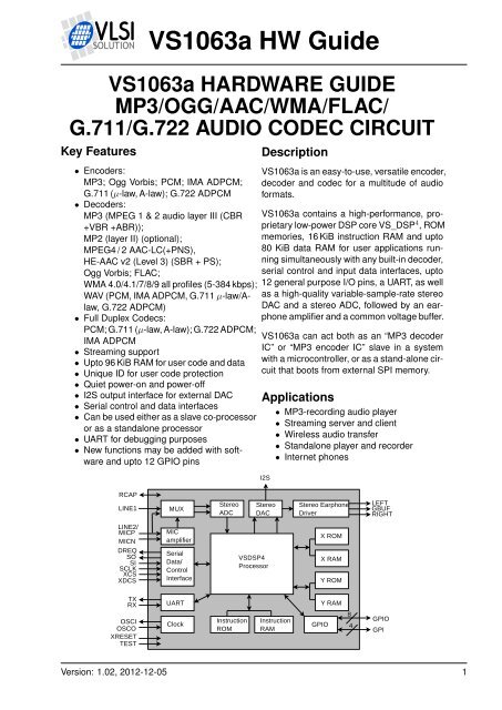
<strong>VS1063</strong>a HW <strong>Guide</strong><strong>VS1063</strong>a HARDWARE GUIDEMP3/OGG/AAC/WMA/FLAC/G.711/G.722 AUDIO CODEC CIRCUITKey Features• Encoders:MP3; Ogg Vorbis; PCM; IMA ADPCM;G.711 (µ-law, A-law); G.722 ADPCM• Decoders:MP3 (MPEG 1 & 2 audio layer III (CBR+VBR +ABR));MP2 (layer II) (optional);MPEG4 / 2 AAC-LC(+PNS),HE-AAC v2 (Level 3) (SBR + PS);Ogg Vorbis; FLAC;WMA 4.0/4.1/7/8/9 all profiles (5-384 kbps);WAV (PCM, IMA ADPCM, G.711 µ-law/Alaw,G.722 ADPCM)• Full Duplex Codecs:PCM; G.711 (µ-law, A-law); G.722 ADPCM;IMA ADPCM• Streaming support• Upto 96 KiB RAM for user code and data• Unique ID for user code protection• Quiet power-on and power-off• I2S output interface for external DAC• Serial control and data interfaces• Can be used either as a slave co-processoror as a standalone processor• UART for debugging purposes• New functions may be added with softwareand upto 12 GPIO pinsDescription<strong>VS1063</strong>a is an easy-to-use, versatile encoder,decoder and codec for a multitude of audioformats.<strong>VS1063</strong>a contains a high-performance, proprietarylow-power DSP core VS_DSP 4 , ROMmemories, 16 KiB instruction RAM and upto80 KiB data RAM for user applications runningsimultaneously with any built-in decoder,serial control and input data interfaces, upto12 general purpose I/O pins, a UART, as wellas a high-quality variable-sample-rate stereoDAC and a stereo ADC, followed by an earphoneamplifier and a common voltage buffer.<strong>VS1063</strong>a can act both as an “MP3 decoderIC” or “MP3 encoder IC” slave in a systemwith a microcontroller, or as a stand-alone circuitthat boots from external SPI memory.Applications• MP3-recording audio player• Streaming server and client• Wireless audio transfer• Standalone player and recorder• Internet phonesVersion: 1.02, 2012-12-05 1
<strong>VS1063</strong>a HW <strong>Guide</strong>Additional Features• EarSpeaker Spatial Processing• Bass & treble controls• Alternatively a 5-channel equalizer• AD Mixer allows monitoring A/D converterinput while listening to stream• PCM Mixer allows inserting a sidestreamwhile listening to main stream• Adjustable Speed Shifter• Operates with a single 12..13 MHz or24..26 MHz clock• Internal PLL clock multiplier• Low-power operation• High-quality on-chip stereo DAC with nophase error between channels• Zero-cross detection for smooth volumechange• Stereo earphone driver capable of drivinga 30 Ω load• Separate voltages for analog, digital, I/O• Lead-free RoHS-compliant packageFurther Description<strong>VS1063</strong>a is a pin-compatible alternative for<strong>VLSI</strong> <strong>Solution</strong>’s VS1053. It has all the functionalityof VS1053 (except MP1 and MIDIdecoding) and many new features, particularlyMP3 and Ogg Vorbis recording.Also full-duplex codec functions for phone applicationshave been added to <strong>VS1063</strong>a.A factory-programmable unique chip ID providesa basis for digital rights management orunit identification features.Operating Modes<strong>VS1063</strong>a operates in one of two host modes:as a slave co-processor or as a standaloneprocessor.When used as a slave co-processor <strong>VS1063</strong>acan operate in three different operation modes:decoder, encoder or codec mode. In decodermode <strong>VS1063</strong>a receives its input bitstreamthrough a serial input bus. The input streamis decoded and passed through an 18-bit digitalvolume control to an oversampling sigmadeltaDAC. Decoding is controlled via a serialcontrol bus. In addition to the basic decoding,it is possible to add application specificfeatures, like DSP effects, to the user RAMmemory, or even to load user applications.In encoder mode <strong>VS1063</strong>a can reads audiofrom its analog inputs, optionally compressesthe data, which can then be read by the hostprocessor. In codec mode <strong>VS1063</strong>a offers afull-duplex audio interface.When used as a standalone processor the<strong>VS1063</strong>a can boot either from SPI EEPROMor FLASH memory. Alternatively code anddata can be provided by a host controller.User CodeUsers can write their own user interface orsignal processing code for the <strong>VS1063</strong>a usingVSIDE (<strong>VLSI</strong> <strong>Solution</strong>’s Integrated DevelopmentEnvironment).As a default, there are 16 KiB of free codeRAM and about 4 KiB of free data RAM foruser applications. Depending on the application,the data RAM can be expanded to thefull 80 KiB that is available in <strong>VS1063</strong>a.Version: 1.02, 2012-12-05 2
<strong>VS1063</strong>a HW <strong>Guide</strong>CONTENTSContents<strong>VS1063</strong> <strong>Hardware</strong> <strong>Guide</strong> Front Page 1Table of Contents 3List of Figures 51 Introduction 62 Disclaimer 63 Definitions 64 The VSDSP Processor Core 75 <strong>VS1063</strong>a Memory Map 86 <strong>VS1063</strong>a <strong>Hardware</strong> Audio Paths 96.1 <strong>VS1063</strong>a <strong>Hardware</strong> DAC Audio Paths . . . . . . . . . . . . . . . . . . . . . . . . 96.2 <strong>VS1063</strong>a <strong>Hardware</strong> ADC Audio Paths . . . . . . . . . . . . . . . . . . . . . . . . 107 <strong>Hardware</strong> Registers 117.1 Serial Control Interface (SCI) . . . . . . . . . . . . . . . . . . . . . . . . . . . . 117.1.1 SCI <strong>Hardware</strong> Registers . . . . . . . . . . . . . . . . . . . . . . . . . 117.1.2 Mode SCI_MODE (RW) . . . . . . . . . . . . . . . . . . . . . . . . . 117.1.3 Status Information SCI_STATUS (RW) . . . . . . . . . . . . . . . . . 127.1.4 SCI Change SCI_CHANGE (R) . . . . . . . . . . . . . . . . . . . . . 137.1.5 SCI Interrupts . . . . . . . . . . . . . . . . . . . . . . . . . . . . . . . 137.2 Serial Data Interface (SDI) . . . . . . . . . . . . . . . . . . . . . . . . . . . . . . 137.2.1 SDI Interrupts . . . . . . . . . . . . . . . . . . . . . . . . . . . . . . . 137.3 Digital-to-Analog Converter (DAC) . . . . . . . . . . . . . . . . . . . . . . . . . . 147.3.1 DAC Registers . . . . . . . . . . . . . . . . . . . . . . . . . . . . . . . 147.3.2 Volume Control DAC_VOL . . . . . . . . . . . . . . . . . . . . . . . . 147.3.3 DAC Interrupts . . . . . . . . . . . . . . . . . . . . . . . . . . . . . . . 147.4 PLL Controller . . . . . . . . . . . . . . . . . . . . . . . . . . . . . . . . . . . . . 157.4.1 PLL Control DAC_FCTLH[13:4] . . . . . . . . . . . . . . . . . . . . . 157.5 General-Purpose Input/Output (GPIO) . . . . . . . . . . . . . . . . . . . . . . . 177.5.1 GPIO Registers . . . . . . . . . . . . . . . . . . . . . . . . . . . . . . 177.6 Interrupt Control . . . . . . . . . . . . . . . . . . . . . . . . . . . . . . . . . . . . 187.6.1 Interrupt Control Registers . . . . . . . . . . . . . . . . . . . . . . . . 187.7 Universal Asynchronous Receiver/Transmitter (UART) . . . . . . . . . . . . . . 197.7.1 UART Registers . . . . . . . . . . . . . . . . . . . . . . . . . . . . . . 197.7.2 Status UART_STATUS . . . . . . . . . . . . . . . . . . . . . . . . . . 197.7.3 Data UART_DATA . . . . . . . . . . . . . . . . . . . . . . . . . . . . . 207.7.4 Data High UART_DATAH . . . . . . . . . . . . . . . . . . . . . . . . . 207.7.5 Divider UART_DIV . . . . . . . . . . . . . . . . . . . . . . . . . . . . 207.7.6 UART Interrupts and Operation . . . . . . . . . . . . . . . . . . . . . 217.8 Timers . . . . . . . . . . . . . . . . . . . . . . . . . . . . . . . . . . . . . . . . . 227.8.1 Timer Registers . . . . . . . . . . . . . . . . . . . . . . . . . . . . . . 227.8.2 Configuration TIMER_CONFIG . . . . . . . . . . . . . . . . . . . . . 227.8.3 Configuration TIMER_ENABLE . . . . . . . . . . . . . . . . . . . . . 23Version: 1.02, 2012-12-05 3
<strong>VS1063</strong>a HW <strong>Guide</strong>CONTENTS7.8.4 Timer X Startvalue TIMER_Tx[L/H] . . . . . . . . . . . . . . . . . . . 237.8.5 Timer X Counter TIMER_TxCNT[L/H] . . . . . . . . . . . . . . . . . . 237.8.6 Timer Interrupts . . . . . . . . . . . . . . . . . . . . . . . . . . . . . . 237.9 I2S DAC Interface . . . . . . . . . . . . . . . . . . . . . . . . . . . . . . . . . . . 247.9.1 I2S Registers . . . . . . . . . . . . . . . . . . . . . . . . . . . . . . . 247.9.2 Configuration I2S_CONFIG . . . . . . . . . . . . . . . . . . . . . . . 247.10 Analog-to-Digital Converter (ADC) . . . . . . . . . . . . . . . . . . . . . . . . . . 257.10.1 ADC Registers . . . . . . . . . . . . . . . . . . . . . . . . . . . . . . 257.10.2 Control ADC_CONTROL . . . . . . . . . . . . . . . . . . . . . . . . . 257.10.3 ADC Interrupts . . . . . . . . . . . . . . . . . . . . . . . . . . . . . . 257.11 Resampler SampleRate Converter (SRC) . . . . . . . . . . . . . . . . . . . . . 267.11.1 SRC Registers . . . . . . . . . . . . . . . . . . . . . . . . . . . . . . 267.11.2 Control SRC_CONTROL . . . . . . . . . . . . . . . . . . . . . . . . . 267.11.3 SRC Interrupts . . . . . . . . . . . . . . . . . . . . . . . . . . . . . . 267.12 Sidestream Sigma-Delta Modulator (SDM) . . . . . . . . . . . . . . . . . . . . . 277.12.1 SDM Registers . . . . . . . . . . . . . . . . . . . . . . . . . . . . . . 277.12.2 Control SDM_CONTROL . . . . . . . . . . . . . . . . . . . . . . . . . 277.12.3 SDM Interrupts . . . . . . . . . . . . . . . . . . . . . . . . . . . . . . 278 Latest Document Version Changes 289 Contact Information 29Version: 1.02, 2012-12-05 4
<strong>VS1063</strong>a HW <strong>Guide</strong>LIST OF FIGURESList of Figures1 <strong>VS1063</strong>a DAC data paths with some data registers . . . . . . . . . . . . . . . . . 92 <strong>VS1063</strong>a ADC data paths with some data registers . . . . . . . . . . . . . . . . . 103 RS232 serial interface protocol . . . . . . . . . . . . . . . . . . . . . . . . . . . . 194 I2S interface, 192 kHz. . . . . . . . . . . . . . . . . . . . . . . . . . . . . . . . . . 24Version: 1.02, 2012-12-05 5
<strong>VS1063</strong>a HW <strong>Guide</strong>3 DEFINITIONS1 IntroductionThis is a hardware guide for the <strong>VS1063</strong>a. Its intent is to provide the reader with sufficientamounts of information to write programs that take over <strong>VS1063</strong>a in part or in whole. It is alsointended to give users a better understanding of the inner workings of <strong>VS1063</strong>a.Because <strong>VS1063</strong>a shares the hardware and register interfaces with the VS1053 and VS8053series audio processors, everything written in this document, unless specifically marked otherwise,is applicable to all of them.2 DisclaimerThis is a preliminary guide. It represents <strong>VLSI</strong> <strong>Solution</strong>’s best attempt at documenting thehardware of <strong>VS1063</strong>a. However, <strong>VLSI</strong> <strong>Solution</strong> is not responsible for any errors, omissions, ormisleading statements in this document.This guide is the second part of a three-part entity, consisting of <strong>VS1063</strong>a Datasheet, <strong>VS1063</strong>a<strong>Hardware</strong> <strong>Guide</strong>, and <strong>VS1063</strong>a Programmer’s <strong>Guide</strong>. To avoid repetition, it is assumed thatthe reader of this guide has already familiarized himself with the <strong>VS1063</strong>a Datasheet.3 DefinitionsABR Average BitRate. Bitrate of stream may vary locally, but will stay close to a given numberwhen averaged over a longer time.B Byte, 8 bits.b Bit.CBR Constant BitRate. Bitrate of stream will be the same for each compression block.Ki “Kibi” = 2 10 = 1024 (IEC 60027-2).Mi “Mebi” = 2 20 = 1048576 (IEC 60027-2).VBR Variable BitRate. Bitrate will vary depending on the complexity of the source material.VSIDE <strong>VLSI</strong> <strong>Solution</strong>’s Integrated Development Environment.VS_DSP <strong>VLSI</strong> <strong>Solution</strong>’s DSP core.W Word. In VS_DSP, instruction words are 32-bit and data words are 16-bit wide.Version: 1.02, 2012-12-05 6
<strong>VS1063</strong>a HW <strong>Guide</strong>4 THE VSDSP PROCESSOR CORE4 The VSDSP Processor CoreVS_DSP is a 16/32-bit DSP processor core that also had extensive all-purpose processor features.<strong>VLSI</strong> <strong>Solution</strong>’s free Integrated Development Environment VSIDE contains all the tools anddocumentation needed to write, simulate and debug Extended ANSI C or Assembly Languageprograms for <strong>VS1063</strong>a.Version: 1.02, 2012-12-05 7
5 <strong>VS1063</strong>a Memory Map<strong>VS1063</strong>a HW <strong>Guide</strong>5 <strong>VS1063</strong>A MEMORY MAPX-memoryAddress Description0x0000..0x17ff System RAM0x1800..0x187f User RAM0x1880..0x197f Stack0x1980..0x3fff System RAM0x4000..0xbfff ROM 32k0xc000..0xc0ff Peripherals0xc100..0xffff ROM 15.75kY-memoryAddress Description0x0000..0x17ff System RAM0x1800..0x187f User RAM0x1880..0x197f Stack0x1980..0x3fff System RAM0x4000..0xdfff ROM 40k0xe000..0xffff System RAMI-memoryAddress Description0x0000..0x0fff RAM0x0050..0x0fff User RAM0x1000..0x1fff -0x2000..0xffff ROM 56kand banked0xc000..0xffff ROM4 16kNote: The <strong>VS1063</strong>a Programmer’s <strong>Guide</strong> has a more accurate software memory map.Version: 1.02, 2012-12-05 8
<strong>VS1063</strong>a HW <strong>Guide</strong>6 <strong>VS1063</strong>A HARDWARE AUDIO PATHS6 <strong>VS1063</strong>a <strong>Hardware</strong> Audio Paths6.1 <strong>VS1063</strong>a <strong>Hardware</strong> DAC Audio PathsRegistersDAC_FCTLLDAC_FCTLHRegisterDAC_VOLRegistersDAC_LEFTDAC_RIGHTDACSRCSigma−deltamodulatorAnalogdriverLeftRightCBUFI2SResamplerSRCSidestreamSDMRegisterSRC_CONTROLRegistersSRC_LEFTSRC_RIGHTRegistersSDM_LEFTSDM_RIGHTRegisterSDM_CONTROLFigure 1: <strong>VS1063</strong>a DAC data paths with some data registersFigure 1 presents the <strong>VS1063</strong>a hardware DAC audio paths.The main audio path starts from the DAC register (Chapter 7.3) to the high-fidelity, fully digitalDAC SRC (Digital-to-Analog Converter SampleRate Converter), which low-pass filters and interpolatesthe data to the high samplerate of XTALI/2 (nominally 6.144 MHz). This 18-bit data isthen fed to the volume control. It then passes through the sigma-delta modulator to the analogdriver and analog Left and Right signals.The user may resample and record the data with the Resampler SampleRate Converter (Chapter7.11). Because there is no automatic low-pass filtering, it is the user’s responsibility to avoidaliasing distortion.The user may add a PCM sidestream with the Sidestream Sigma-Delta Modulator input (Chapter7.12). As is the case with the Resampler SampleRate Converter, hardware doesn’t offerlow-pass filtering, so sufficient aliasing image rejection is the responsibility of the user.Version: 1.02, 2012-12-05 9
<strong>VS1063</strong>a HW <strong>Guide</strong>6 <strong>VS1063</strong>A HARDWARE AUDIO PATHS6.2 <strong>VS1063</strong>a <strong>Hardware</strong> ADC Audio PathsMICNMICPMicrophoneamplifierLINE1LINE2MultiplexerADCADCdecimatorRegistersADC_DATA_LEFTADC_DATA_RIGHTFigure 2: <strong>VS1063</strong>a ADC data paths with some data registersFigure 1 presents the <strong>VS1063</strong>a hardware ADC audio paths.Analog audio may be fed upto two channels: one as a differential signal to MICN/MICP or as aone-sided signal to Line1, and the other as a one-sided signal to Line2.If microphone input for the left channel has been selected, audio is fed through a microphoneamplifier and that signal is selected by a multiplexer.Audio is then downsampled to one of four allowed samplerates: XTALI/64, XTALI/128, XTALI/256or XTALI/512. With the nominal 12.288 MHz crystal, these correspond to 192, 96, 48 or 24 kHzsamplerates, respectively (Chapter 7.12).If the “3 MHz” option bit SS_AD_CLOCK in register SCI_STATUS has been set to 1, thensamplerates are divided by two, so the nominal samplerates become 96, 48, 24 and 12 kHz.Version: 1.02, 2012-12-05 10
7 <strong>Hardware</strong> Registers<strong>VS1063</strong>a HW <strong>Guide</strong>7 HARDWARE REGISTERS<strong>VS1063</strong>a registers are memory mapped to X data memory, starting from address 0xC000.7.1 Serial Control Interface (SCI)SCI registers are mapped to X memory addresses between 0xC000..0xC00F. In addition tothese registers, there is one in address 0xC010, called SCI_CHANGE.Only 3 of these 17 registers contain direct hardware control. Those registers and their hardwareregisters bits are described in this section. For documentation of the software register bits, seethe <strong>VS1063</strong>a Datasheet.7.1.1 SCI <strong>Hardware</strong> RegistersSCI registersReg Type Reset Abbrev[bits] Description0xC000 rw 0x4000 2 SCI_MODE Mode control0xC001 rw 0x000C 2 SCI_STATUS Status of <strong>VS1063</strong>a0xC010 r 0x00 SCI_CHANGE[5:0] Last SCI access address1 Firmware changes the value of this register immediately to 0x4800.2 Firmware changes the value of this register immediately to 0x48 (analog enabled), and aftera short while to 0x40 (analog drivers enabled).7.1.2 Mode SCI_MODE (RW)SCI_MODE bitsName Bit Function Value DescriptionSM_DACT 8 DCLK active edge 0 rising1 fallingSM_SDIORD 9 SDI bit order 0 MSb first1 MSb lastSM_SDISHARE 10 Share SPI chip select 0 no1 yesSM_SDINEW 11 VS1002 native SPI modes 0 no1 yesSM_LINE1 14 MIC / LINE1 selector 0 MICP1 LINE1SM_CLK_RANGE 15 Input clock range 0 12..13 MHz1 24..26 MHzVersion: 1.02, 2012-12-05 11
<strong>VS1063</strong>a HW <strong>Guide</strong>7 HARDWARE REGISTERSSM_DACT defines the active edge of data clock for SDI. When ’0’, data is read at the risingedge, when ’1’, data is read at the falling edge.When SM_SDIORD is clear, bytes on SDI are sent MSb first. By setting SM_SDIORD, the usermay reverse the bit order for SDI, i.e. bit 0 is received first and bit 7 last. Bytes are, however,still sent in the default order. This register bit has no effect on the SCI bus.Setting SM_SDISHARE and SM_SDINEW makes SCI and SDI share the same chip select.Setting SM_SDINEW will activate VS1002 native serial modes. Note, that this bit is set as adefault when <strong>VS1063</strong>a is started up.SM_LINE_IN is used to select the left-channel input for ADPCM recording. If ’0’, differentialmicrophone input pins MICP and MICN are used; if ’1’, line-level MICP/LINEIN1 pin is used.SM_CLK_RANGE activates a clock divider in the XTAL input. When SM_CLK_RANGE is set,the clock is divided by 2 at the input. From the chip’s point of view e.g. 24 MHz becomes12 MHz. SM_CLK_RANGE should be set as soon as possible after a chip reset.7.1.3 Status Information SCI_STATUS (RW)SCI_STATUS contains information on the current status of <strong>VS1063</strong>a. It also controls somelow-level things that the user does not usually have to care about.SCI_STATUS bitsName Bits DescriptionSS_SWING 14:12 Set swing to +0 dB, +0.5 dB, .., or +3.5 dBSS_VCM_OVERLOAD 11 GBUF overload indicator ’1’ = overloadSS_VCM_DISABLE 10 GBUF overload detection ’1’ = disableSS_APDOWN2 3 Analog driver powerdownSS_APDOWN1 2 Analog internal powerdownSS_AD_CLOCK 1 AD clock select, ’0’ = 6 MHz, ’1’ = 3 MHzSS_REFERENCE_SEL 0 Reference voltage selection, ’0’ = 1.23 V, ’1’ = 1.65 VIf AVDD is higher at least 3.3 V, SS_REFERENCE_SEL can be set to select 1.65 V referencevoltage to increase the analog output swing.SS_AD_CLOCK can be set to divide the AD modulator frequency by 2 if XTALI/2 is too much.SS_APDOWN2 controls analog driver powerdown. SS_APDOWN1 controls internal analogpowerdown. These bit are meant to be used by the system firmware only.<strong>VS1063</strong>a contains GBUF protection circuit which disconnects the GBUF driver when too muchcurrent is drawn, indicating a short-circuit to ground. SS_VCM_OVERLOAD is high while theoverload is detected. SS_VCM_DISABLE can be set to disable the protection feature.Version: 1.02, 2012-12-05 12
<strong>VS1063</strong>a HW <strong>Guide</strong>7 HARDWARE REGISTERSSS_SWING allows you to go above the 0 dB volume setting. Value 0 is normal mode, 1 gives+0.5 dB, and 2 gives +1.0 dB. Settings from 3 to 7 cause the DAC modulator to be overdrivenand should not be used. You can use SS_SWING with I2S to control the amount of headroom.7.1.4 SCI Change SCI_CHANGE (R)SCI_CHANGE bitsName Bits DescriptionSCI_CH_WRITE 4 1 if last access was a write cycleSCI_CH_ADDR 3:0 SCI address of last accessSCI_CHANGE contains the last SCI register that has been accessed through the SCI bus, aswell as whether the access was a read or write operation.7.1.5 SCI InterruptsWhenever an external SPI read from or write to an SCI register is done, an SCI interrupt isgenerated. The interrupt routine can then check SCI_CHANGE to see which SCI register wasaccessed and whether the access was a read or write operation.7.2 Serial Data Interface (SDI)Whenever two bytes have been written to the SDI bus, an interrupt is generated and the datacan be read as a 16-bit big-endian value from the SDI registers. The user can control the DREQpin as if it was a general-purpose output through its own register bit.SDI registersReg Type Reset Abbrev[bits] Description0xC011 r x SDI_DATA Last received 2 bytes, big-endian0xC012 w 0 SDI_DREQ[0] DREQ pin control7.2.1 SDI InterruptsEach time a new byte pair has been received, an SDI interrupt is generated.Version: 1.02, 2012-12-05 13
<strong>VS1063</strong>a HW <strong>Guide</strong>7 HARDWARE REGISTERS7.3 Digital-to-Analog Converter (DAC)7.3.1 DAC RegistersDAC registersReg Type Reset Abbrev[bits] Description0xC013 rw 0 DAC_FCTLL DAC samplerate control, 16 LSbs0xC014 rw 0 DAC_FCTLH DAC samplerate control 4 MSbs, PLL control0xC015 rw 0 DAC_LEFT DAC left channel PCM value0xC016 rw 0 DAC_RIGHT DAC right channel PCM value0xC045 rw 0 DAC_VOL DAC hardware volumeThe internal 20-bit register DAC_FCTL is calculated from DAC_FCTLH and DAC_FCTLL registersas follows: DAC_FCTL = (DAC_FCTLH & 15) × 65536 + DAC_FCTLL. Highest supportedvalue for DAC_FCTL is 0x80000.If we define C = DAC_FCTL and X = XTALI in Hz, then the resulting samplerate f s of the associatedDAC SampleRate Converter is f s = C × X × 2 −27 .Example:If C = 0x80000 and X = 12.288 MHz then f s = 524288 × (12.288 × 10 6 ) × 2 −27 = 48000 (Hz).Note: FCTLH bits 13:4 are used for the PLL Controller. See Chapter 7.4 for details.7.3.2 Volume Control DAC_VOLDAC_VOL bitsName Bits DescriptionLEFT_FINE 15:12 Left channel gain +0.0 dB. . .+5.5 dB (0 to 11)LEFT_COARSE 11:8 Left channel attenuation in -6 dB stepsRIGHT_FINE 7:4 Right channel volume +0.0 dB. . .+5.5 dB (0 to11)RIGHT_COARSE 3:0 Right channel attenuation in -6 dB stepsNormally DAC_VOL is handled by the firmware. DAC_VOL depends on the software registerSCI_VOL and the bass and treble settings in SCI_BASS (and optionally SS_SWING bits inSCI_STATUS).7.3.3 DAC InterruptsWhenever a new stereo sample has been sent out and a new value is required, a DAC interruptis generated.Version: 1.02, 2012-12-05 14
<strong>VS1063</strong>a HW <strong>Guide</strong>7 HARDWARE REGISTERS7.4 PLL ControllerThe Phase-Locked Loop (PLL) controller is used to generate clock frequencies that are higherthan the incoming (crystal-based) clock frequency. The PLL output is used by the CPU coreand some peripherals.Configurable features include:• VCO Enable/Disable• Select VCO or input clock to be output clock• Route VCO frequency to output pin• Select PLL clock multiplierAt the core of the PLL controller is the VCO, a high frequency oscillator, whose oscillationfrequency is adjusted to be an integer multiple of some input frequency. As the name “Phase-Locked Loop” suggests, this is done by comparing the phase of the input frequency against thephase of a signal which is derived from the VCO output through frequency division.If the system is stable, e.g. the comparison phase difference remains virtually zero, the PLL issaid to be “in lock”. This means that the output frequency of the VCO is stable and reliable.The PLL is preceded by a division-by-two unit. Thus, with a nominal XTALI = 12.288 MHz, theinternal clock frequency CLKI can be adjusted with an accuracy of XTALI/2 = 6.144 MHz.7.4.1 PLL Control DAC_FCTLH[13:4]PLL control lies in DAC_FCTL bits 13:4. To see what bits 3:0 do, see Chapter 7.3.FREQCTLH PLL bitsName Bits DescriptionFCH_PLL_LOCKED 13 0=lock failed since last test (read-only)FCH_PLL_SET_LOCK 12 1:Sets FCH_PLL_LOCKED to 1 to start lock testFCH_PLL_VCO_OUT_ENA 11 Route VCO to GPIO pin (VS1000:second cs pin)FCH_PLL_FORCE_PLL 9 1:System clock is VCO / 0:System clock is inclkFCH_PLL_DIV_INCLK 8 divide inclk by 2 (for 1.5, 2.5 or 3.5 x clk)FCH_PLL_RATE 7:4 PLL rate controlThe PLL locked status can be checked by generating a high-active pulse (writing first “1” , then“0”) to FCH_PLL_SET_LOCK and reading FCH_PLL_LOCKED. FCH_PLL_LOCKED is set to“1” along with the high level of FCH_PLL_SET_LOCK and to “0” whenever the PLL falls out oflock. So if the “1” remains in FCH_PLL_LOCKED, PLL is in sync.Version: 1.02, 2012-12-05 15
<strong>VS1063</strong>a HW <strong>Guide</strong>7 HARDWARE REGISTERSThe PLL controller’s operation is optimized for frequencies around 12. . . 13 MHz. If you use an24. . . 26 MHz input clock, set the extra clock divider bit SM_CLK_RANGE in register SCI_MODEto 1 before activating the PLL.It’s recommended to change the PLL rate in small steps and wait for the PLL to stabilize aftereach change. For diagnostic purposes, the PLL clock output (VCO) can be routed to an I/O pinso it can be scanned with an oscilloscope.FCH_PLL_RATE (bits 7:4) control PLL multiplication rate. PLL multiplier is (FCH_PLL_RATE+ 1). When FCH_PLL_RATE is 0, the VCO is powered down and output clock is forced to beinput clock (same as if FCH_PLL_FORCE_PLL = 0).Version: 1.02, 2012-12-05 16
<strong>VS1063</strong>a HW <strong>Guide</strong>7 HARDWARE REGISTERS7.5 General-Purpose Input/Output (GPIO)7.5.1 GPIO RegistersGPIO registersReg Type Reset Abbrev[bits] Description0xC017 rw 0 GPIO_DDR[9:0] Direction0xC018 r 0 GPIO_IDATA[11:0] Values read from the pins0xC019 rw 0 GPIO_ODATA[8:0] Values set to the pinsGPIO_DIR is used to set the direction of the GPIO pins. 1 means output. GPIO_ODATAremembers its values even if a GPIO_DIR bit is set to input.GPIO_IDATA is used to read the pin states. In <strong>VS1063</strong> also the SDI and SCI input pinscan be read through GPIO_IDATA: SCLK = GPIO_IDATA[8], XCS = GPIO_IDATA[9], SI =GPIO_IDATA[10], and XDCS = GPIO_IDATA[11].GPIO registers don’t generate interrupts.Note that in <strong>VS1063</strong>a the VSDSP registers can be read and written through the SCI_WRAMADDRand SCI_WRAM registers. You can thus use the GPIO pins quite conveniently.Version: 1.02, 2012-12-05 17
<strong>VS1063</strong>a HW <strong>Guide</strong>7 HARDWARE REGISTERS7.6 Interrupt Control7.6.1 Interrupt Control RegistersInterrupt registersReg Type Reset Abbrev[bits] Description0xC01A rw 0 INT_ENABLE[9:0] Interrupt enable0xC01B w 0 INT_GLOB_DIS[-] Write to add to interrupt counter0xC01C w 0 INT_GLOB_ENA[-] Write to subtract from interrupt counter0xC01D r 0 INT_COUNTER[3:0] Interrupt counterINT_ENABLE controls the interrupts. The control bits are as follows:INT_ENABLE bitsName Bits DescriptionINT_EN_SDM 9 Enable Sigma Delta Modulator interruptINT_EN_SRC 8 Enable SampleRate Converter interruptINT_EN_TIM1 7 Enable Timer 1 interruptINT_EN_TIM0 6 Enable Timer 0 interruptINT_EN_RX 5 Enable UART RX interruptINT_EN_TX 4 Enable UART TX interruptINT_EN_ADC 3 Enable ADC interruptINT_EN_SDI 2 Enable SDI interruptINT_EN_SCI 1 Enable SCI interruptINT_EN_DAC 0 Enable DAC interruptNote: It may take upto 6 clock cycles before changing INT_ENABLE has any effect.Writing any value to INT_GLOB_DIS adds one to the interrupt counter INT_COUNTER andeffectively disables all interrupts. It may take upto 6 clock cycles before writing to this registerhas any effect.Writing any value to INT_GLOB_ENA subtracts one from the interrupt counter INT_COUNTER,unless it already was 0, in which case nothing happens. If, after the operation INT_COUNTERbecomes zero, interrupts selected with INT_ENABLE are restored. An interrupt routine shouldalways write to this register as the last thing it does, because interrupts automatically add oneto the interrupt counter, but subtracting it back to its initial value is the responsibility of the user.It may take upto 6 clock cycles before writing this register has any effect.By reading INT_COUNTER the user may check if the interrupt counter is correct or not. If theregister is not 0, interrupts are disabled.Version: 1.02, 2012-12-05 18
<strong>VS1063</strong>a HW <strong>Guide</strong>7 HARDWARE REGISTERS7.7 Universal Asynchronous Receiver/Transmitter (UART)RS232 UART implements a serial interface using rs232 standard.Startbit D0 D1 D2 D3 D4 D5 D6 D7 StopbitFigure 3: RS232 serial interface protocolWhen the line is idling, it stays in logic high state. When a byte is transmitted, the transmissionbegins with a start bit (logic zero) and continues with data bits (LSB first) and ends up with astop bit (logic high). 10 bits are sent for each 8-bit byte frame.7.7.1 UART RegistersUART registersReg Type Reset Abbrev[bits] Description0xC028 r 0 UART_STATUS[4:0] Status0xC029 r/w 0 UART_DATA[7:0] Data0xC02A r/w 0 UART_DATAH[15:8] Data High0xC02B r/w 0 UART_DIV Divider7.7.2 Status UART_STATUSA read from the status register returns the transmitter and receiver states.UART_STATUS bitsName Bits DescriptionUART_ST_FRAMEERR 4 Framing error (stop bit was 0)UART_ST_RXORUN 3 Receiver overrunUART_ST_RXFULL 2 Receiver data register fullUART_ST_TXFULL 1 Transmitter data register fullUART_ST_TXRUNNING 0 Transmitter runningUART_ST_FRAMEERR is set if the stop bit of the received byte was 0.UART_ST_RXORUN is set if a received byte overwrites unread data when it is transferred fromthe receiver shift register to the data register, otherwise it is cleared.UART_ST_RXFULL is set if there is unread data in the data register.UART_ST_TXFULL is set if a write to the data register is not allowed (data register full).Version: 1.02, 2012-12-05 19
<strong>VS1063</strong>a HW <strong>Guide</strong>7 HARDWARE REGISTERSUART_ST_TXRUNNING is set if the transmitter shift register is in operation.7.7.3 Data UART_DATAA read from UART_DATA returns the received byte in bits 7:0, bits 15:8 are returned as ’0’. Ifthere is no more data to be read, the receiver data register full indicator will be cleared.A receive interrupt will be generated when a byte is moved from the receiver shift register tothe receiver data register.A write to UART_DATA sets a byte for transmission. The data is taken from bits 7:0, otherbits in the written value are ignored. If the transmitter is idle, the byte is immediately movedto the transmitter shift register, a transmit interrupt request is generated, and transmission isstarted. If the transmitter is busy, the UART_ST_TXFULL will be set and the byte remains in thetransmitter data register until the previous byte has been sent and transmission can proceed.7.7.4 Data High UART_DATAHThe same as UART_DATA, except that bits 15:8 are used.7.7.5 Divider UART_DIVUART_DIV bitsName Bits DescriptionUART_DIV_D1 15:8 Divider 1 (0..255)UART_DIV_D2 7:0 Divider 2 (6..255)The divider is set to 0x0000 in reset. The ROM boot code must initialize it correctly dependingon the master clock frequency to get the correct bit speed. The second divider (D 2 ) must befrom 6 to 255.The communication speed f =the TX/RX speed in bps.f m(D 1 +1)×(D 2 ) , where f m is the master clock frequency, and f isVersion: 1.02, 2012-12-05 20
<strong>VS1063</strong>a HW <strong>Guide</strong>7 HARDWARE REGISTERSExample divider values for common communication speeds at 49.152 MHz master clock:Example UART speeds, f m = 49.152 MHzComm. Speed [bps] UART_DIV_D1 UART_DIV_D24800 255 409600 255 2014400 233 1519200 255 1028800 243 738400 159 857600 121 7115200 60 77.7.6 UART Interrupts and OperationTransmitter operates as follows: After an 8-bit word is written to the transmit data register it willbe transmitted instantly if the transmitter is not busy transmitting the previous byte. When thetransmission begins a TX_INTR interrupt will be sent. Status bit [1] informs the transmitter dataregister empty (or full state) and bit [0] informs the transmitter (shift register) empty state. Anew word must not be written to transmitter data register if it is not empty (bit [1] = ’0’). Thetransmitter data register will be empty as soon as it is shifted to transmitter and the transmissionis started. It is safe to write a new word to transmitter data register every time a transmit interruptis generated.Receiver operates as follows: It samples the RX signal line and if it detects a high to lowtransition, a start bit is found. After this it samples each 8 bit at the middle of the bit time (usinga constant timer), and fills the receiver (shift register) LSB first. Finally the data in the receiveris moved to the reveive data register, the stop bit state is checked (logic high = ok, logic low =framing error) for status bit[4], the RX_INTR interrupt is sent, status bit[2] (receive data registerfull) is set, and status bit[2] old state is copied to bit[3] (receive data overrun). After that thereceiver returns to idle state to wait for a new start bit. Status bit[2] is zeroed when the receiverdata register is read.RS232 communication speed is set using two clock dividers. The base clock is the processormaster clock. Bits 15-8 in these registers are for first divider and bits 7-0 for second divider. RXsample frequency is the clock frequency that is input for the second divider.Version: 1.02, 2012-12-05 21
<strong>VS1063</strong>a HW <strong>Guide</strong>7 HARDWARE REGISTERS7.8 TimersThere are two 32-bit timers that can be initialized and enabled independently of each other. Ifenabled, a timer initializes to its start value, written by a processor, and starts decrementingevery clock cycle. When the value goes past zero, an interrupt is sent, and the timer initializesto the value in its start value register, and continues downcounting. A timer stays in that loopas long as it is enabled.A timer has a 32-bit timer register for down counting and a 32-bit register for holding the timerstart value written by the processor. Timers have also a 2-bit TIMER_ENA register. Each timeris enabled (1) or disabled (0) by a corresponding bit of the enable register.7.8.1 Timer RegistersTimer registersReg Type Reset Abbrev[bits] Description0xC030 r/w 0 TIMER_CONFIG[7:0] Timer configuration0xC031 r/w 0 TIMER_ENABLE[1:0] Timer enable0xC034 r/w 0 TIMER_T0L Timer0 startvalue - LSBs0xC035 r/w 0 TIMER_T0H Timer0 startvalue - MSBs0xC036 r/w 0 TIMER_T0CNTL Timer0 counter - LSBs0xC037 r/w 0 TIMER_T0CNTH Timer0 counter - MSBs0xC038 r/w 0 TIMER_T1L Timer1 startvalue - LSBs0xC039 r/w 0 TIMER_T1H Timer1 startvalue - MSBs0xC03A r/w 0 TIMER_T1CNTL Timer1 counter - LSBs0xC03B r/w 0 TIMER_T1CNTH Timer1 counter - MSBs7.8.2 Configuration TIMER_CONFIGTIMER_CONFIG bitsName Bits DescriptionTIMER_CF_CLKDIV 7:0 Master clock dividerTIMER_CF_CLKDIV is the master clock divider for all timer clocks. The generated internalclock frequency f i = fmc+1 , where f m is the master clock frequency and c is TIMER_CF_CLKDIV.Example: With a 12 MHz master clock, TIMER_CF_DIV=3 divides the master clock by 4, andthe output/sampling clock would thus be f i = 12MHz3+1= 3MHz.Version: 1.02, 2012-12-05 22
7.8.3 Configuration TIMER_ENABLE<strong>VS1063</strong>a HW <strong>Guide</strong>7 HARDWARE REGISTERSTIMER_ENABLE bitsName Bits DescriptionTIMER_EN_T1 1 Enable timer 1TIMER_EN_T0 0 Enable timer 07.8.4 Timer X Startvalue TIMER_Tx[L/H]The 32-bit start value TIMER_Tx[L/H] sets the initial counter value when the timer is reset. Thetimer interrupt frequency f t =f ic+1 where f i is the master clock obtained with the clock divider(see Chapter 7.8.2 and c is TIMER_Tx[L/H].Example: With a 12 MHz master clock and with TIMER_CF_CLKDIV=3, the master clock f i =3MHz. If TIMER_TH=0, TIMER_TL=99, then the timer interrupt frequency f t = 3MHz99+1=30kHz.7.8.5 Timer X Counter TIMER_TxCNT[L/H]TIMER_TxCNT[L/H] contains the current counter values. By reading this register pair, the usermay get knowledge of how long it will take before the next timer interrupt. Also, by writing tothis register, a one-shot different length timer interrupt delay may be realized.7.8.6 Timer InterruptsEach timer has its own interrupt, which is asserted when the timer counter underflows.Version: 1.02, 2012-12-05 23
<strong>VS1063</strong>a HW <strong>Guide</strong>7 HARDWARE REGISTERS7.9 I2S DAC InterfaceThe I2S DAC Interface makes it possible to attach an external DAC to the system.Note: The samplerate of the audio file and the I2S rate are independent. All audio will beautomatically converted to 6.144 MHz for <strong>VS1063</strong> DAC and to the configured I2S rate using ahigh-quality sample-rate converter.Note: In <strong>VS1063</strong>a the I2S pins share different GPIO pins than in VS1033 to be able to use SPIboot and I2S in the same application.7.9.1 I2S RegistersI2S registersReg Type Reset Abbrev[bits] Description0xC040 r/w 0 I2S_CONFIG[3:0] I2S configuration7.9.2 Configuration I2S_CONFIGI2S_CONFIG bitsName Bits DescriptionI2S_CF_MCLK_ENA 3 Enables the MCLK output (12.288 MHz)I2S_CF_ENA 2 Enables I2S, otherwise pins are GPIOI2S_CF_SRATE 1:0 I2S rate, "10" = 192, "01" = 96, "00" = 48 kHzI2S_CF_ENA enables the I2S interface. After reset I2S is disabled and the pins are used forGPIO inputs.I2S_CF_MCLK_ENA enables the MCLK output. The frequency is either directly the input clock(nominal 12.288 MHz), or half the input clock when mode register bit SM_CLK_RANGE is setto 1 (24-26 MHz input clock).I2S_CF_SRATE controls the output samplerate. When set to 48 kHz, SCLK is MCLK dividedby 8, when 96 kHz SCLK is MCLK divided by 4, and when 192 kHz SCLK is MCLK divided by2. I2S_CF_SRATE can only be changed when I2S_CF_ENA is 0.MCLKSCLKLROUTSDATAMSB LSB MSBLeft Channel WordRight Channel WordFigure 4: I2S interface, 192 kHz.To enable I2S first write 0xc017 to SCI_WRAMADDR and 0xf0 to SCI_WRAM, then write0xc040 to SCI_WRAMADDR and 0x0c to SCI_WRAM.Version: 1.02, 2012-12-05 24
<strong>VS1063</strong>a HW <strong>Guide</strong>7 HARDWARE REGISTERS7.10 Analog-to-Digital Converter (ADC)7.10.1 ADC RegistersADC modulator registers control Analog-to-Digital conversions of <strong>VS1063</strong>a.ADC Decimator registersReg Type Reset Abbrev[bits] Description0xC042 rw 0 ADC_CONTROL[4:0] ADC control0xC043 r 0 ADC_DATA_LEFT ADC left channel data0xC044 r 0 ADC_DATA_RIGHT ADC right channel data7.10.2 Control ADC_CONTROLADC_CONTROL controls the ADC and its associated decimator unit.ADC_CONTROL bitsName Bits DescriptionADC_MODU2_PD 4 Right channel powerdownADC_MODU1_PD 3 Left channel powerdownADC_DECIM_FACTOR 2:1 ADC Decimator factor:- 3 = downsample to XTALI/512 (nominal 24 kHz)- 2 = downsample to XTALI/256 (nominal 48 kHz)- 1 = downsample to XTALI/128 (nominal 96 kHz)- 0 = downsample to XTALI/64 (nominal 192 kHz)ADC_ENABLE 0 Set to activate ADC converter and decimatorNote: Setting bit SS_AD_CLOCK in register SCI_STATUS will halve the operation speed of theA/D unit, and thus halve the resulting samplerate.7.10.3 ADC InterruptsEach time a new (stereo) sample has been generated, an ADC interrupt is generated.Version: 1.02, 2012-12-05 25
<strong>VS1063</strong>a HW <strong>Guide</strong>7 HARDWARE REGISTERS7.11 Resampler SampleRate Converter (SRC)The resampler SRC makes it possible to catch audio from the DAC path.Note: hardware makes no attempts at low-pass filtering data. If the SRC samplerate is lowerthan the DAC samplerate, aliasing may and will occur.7.11.1 SRC RegistersResampler SRC registersReg Type Reset Abbrev[bits] Description0xC046 rw 0 SRC_CONTROL[12:0] SRC control0xC047 r 0 SRC_DATA_LEFT SRC left channel data0xC048 r 0 SRC_DATA_RIGHT SRC right channel data7.11.2 Control SRC_CONTROLSRC_CONTROL BitsName Bits DescriptionSRC_ENABLE 12 Set to enable SRCSRC_DIV 11:0 Set samplerate to XTALI/2/(SRC_DIV+1)7.11.3 SRC InterruptsEach time a new (stereo) sample has been generated, an SRC interrupt is generated.Version: 1.02, 2012-12-05 26
<strong>VS1063</strong>a HW <strong>Guide</strong>7 HARDWARE REGISTERS7.12 Sidestream Sigma-Delta Modulator (SDM)The Sidestream Sigma-Delta Modulator makes it possible to insert a digital side stream on topof existing audio.Note: The SDM provides a direct, low-delay side channel to the Sigma-Delta DACs of VS10xx.It makes no attempts at low-pass filtering data. Thus there will be practically no image rejection.If using low samplerates, this may cause audible aliasing distortion.7.12.1 SDM RegistersSidestream SDM registersReg Type Reset Abbrev[bits] Description0xC049 rw 0 SDM_CONTROL[12:0] SDM control0xC04A rw 0 SDM_DATA_LEFT SDM left channel data0xC04B rw 0 SDM_DATA_RIGHT SDM right channel data7.12.2 Control SDM_CONTROLSDM_CONTROL BitsName Bits DescriptionSDM_ENABLE 12 Set to enable SDMSDM_DIV 11:0 Set samplerate to XTALI/2/(SDM_DIV+1)7.12.3 SDM InterruptsEach time a new (stereo) sample is needed, an SDM interrupt is generated.Version: 1.02, 2012-12-05 27
<strong>VS1063</strong>a HW <strong>Guide</strong>8 LATEST DOCUMENT VERSION CHANGES8 Latest Document Version ChangesThis chapter describes the most important changes to this document.Version 1.02, 2012-12-05• Minor corrections.• Removed preliminary status.Version 0.40, 2011-09-02• Minor corrections.Version 0.30, 2011-05-05• First published release of the guide.Version: 1.02, 2012-12-05 28
<strong>VS1063</strong>a HW <strong>Guide</strong>9 CONTACT INFORMATION9 Contact Information<strong>VLSI</strong> <strong>Solution</strong> OyEntrance G, 2nd floorHermiankatu 8FI-33720 TampereFINLANDFax: +358-3-3140-8288Phone: +358-3-3140-8200Email: sales@vlsi.fiURL: http://www.vlsi.fi/Version: 1.02, 2012-12-05 29