
You also want an ePaper? Increase the reach of your titles
YUMPU automatically turns print PDFs into web optimized ePapers that Google loves.
<strong>VS1003</strong>CONTENTS10.4 SCI Registers . . . . . . . . . . . . . . . . . . . . . . . . . . . . . . . . . . . . . 4510.5 Serial Data Registers . . . . . . . . . . . . . . . . . . . . . . . . . . . . . . . . . 4610.6 DAC Registers . . . . . . . . . . . . . . . . . . . . . . . . . . . . . . . . . . . . . 4710.7 GPIO Registers . . . . . . . . . . . . . . . . . . . . . . . . . . . . . . . . . . . . 4710.8 Interrupt Registers . . . . . . . . . . . . . . . . . . . . . . . . . . . . . . . . . . 4810.9 A/D Modulator Registers . . . . . . . . . . . . . . . . . . . . . . . . . . . . . . . 4910.10 Watchdog v1.0 2002-08-26 . . . . . . . . . . . . . . . . . . . . . . . . . . . . . . 5010.10.1 Registers . . . . . . . . . . . . . . . . . . . . . . . . . . . . . . . . . . 5010.11 UART v1.0 2002-04-23 . . . . . . . . . . . . . . . . . . . . . . . . . . . . . . . . . 5110.11.1 Registers . . . . . . . . . . . . . . . . . . . . . . . . . . . . . . . . . . 5110.11.2 Status UARTx_STATUS . . . . . . . . . . . . . . . . . . . . . . . . . 5110.11.3 Data UARTx_DATA . . . . . . . . . . . . . . . . . . . . . . . . . . . . 5210.11.4 Data High UARTx_DATAH . . . . . . . . . . . . . . . . . . . . . . . . 5210.11.5 Divider UARTx_DIV . . . . . . . . . . . . . . . . . . . . . . . . . . . . 5210.11.6 Interrupts and Operation . . . . . . . . . . . . . . . . . . . . . . . . . 5310.12 Timers v1.0 2002-04-23 . . . . . . . . . . . . . . . . . . . . . . . . . . . . . . . . 5410.12.1 Registers . . . . . . . . . . . . . . . . . . . . . . . . . . . . . . . . . . 5410.12.2 Configuration TIMER_CONFIG . . . . . . . . . . . . . . . . . . . . . 5410.12.3 Configuration TIMER_ENABLE . . . . . . . . . . . . . . . . . . . . . 5510.12.4 Timer X Startvalue TIMER_Tx[L/H] . . . . . . . . . . . . . . . . . . . 5510.12.5 Timer X Counter TIMER_TxCNT[L/H] . . . . . . . . . . . . . . . . . . 5510.12.6 Interrupts . . . . . . . . . . . . . . . . . . . . . . . . . . . . . . . . . 5510.13 System Vector Tags . . . . . . . . . . . . . . . . . . . . . . . . . . . . . . . . . . 5610.13.1 AudioInt, 0x20 . . . . . . . . . . . . . . . . . . . . . . . . . . . . . . . 5610.13.2 SciInt, 0x21 . . . . . . . . . . . . . . . . . . . . . . . . . . . . . . . . 5610.13.3 DataInt, 0x22 . . . . . . . . . . . . . . . . . . . . . . . . . . . . . . . 5610.13.4 ModuInt, 0x23 . . . . . . . . . . . . . . . . . . . . . . . . . . . . . . . 5610.13.5 TxInt, 0x24 . . . . . . . . . . . . . . . . . . . . . . . . . . . . . . . . . 5710.13.6 RxInt, 0x25 . . . . . . . . . . . . . . . . . . . . . . . . . . . . . . . . 5710.13.7 Timer0Int, 0x26 . . . . . . . . . . . . . . . . . . . . . . . . . . . . . . 5710.13.8 Timer1Int, 0x27 . . . . . . . . . . . . . . . . . . . . . . . . . . . . . . 5710.13.9 UserCodec, 0x0 . . . . . . . . . . . . . . . . . . . . . . . . . . . . . . 5810.14 System Vector Functions . . . . . . . . . . . . . . . . . . . . . . . . . . . . . . . 5810.14.1 WriteIRam(), 0x2 . . . . . . . . . . . . . . . . . . . . . . . . . . . . . 5810.14.2 ReadIRam(), 0x4 . . . . . . . . . . . . . . . . . . . . . . . . . . . . . 5810.14.3 DataBytes(), 0x6 . . . . . . . . . . . . . . . . . . . . . . . . . . . . . 5910.14.4 GetDataByte(), 0x8 . . . . . . . . . . . . . . . . . . . . . . . . . . . . 5910.14.5 GetDataWords(), 0xa . . . . . . . . . . . . . . . . . . . . . . . . . . . 5910.14.6 Reboot(), 0xc . . . . . . . . . . . . . . . . . . . . . . . . . . . . . . . 5911 Document Version Changes 6012 Contact Information 61Version: 1.06, 2012-03-16 4
<strong>VS1003</strong>LIST OF FIGURESList of Figures1 Measured ADC performance of the LINEIN pin. . . . . . . . . . . . . . . . . . . . 102 Measured ADC performance of the MIC pins (differential). . . . . . . . . . . . . . 103 Measured performance of RIGHT (or LEFT) output. . . . . . . . . . . . . . . . . 114 Typical spectrum of RIGHT (or LEFT) output. . . . . . . . . . . . . . . . . . . . . 115 Pin Configuration, LQFP-48. . . . . . . . . . . . . . . . . . . . . . . . . . . . . . 126 Pin Configuration, BGA-49. . . . . . . . . . . . . . . . . . . . . . . . . . . . . . . 127 Typical Connection Diagram Using LQFP-48. . . . . . . . . . . . . . . . . . . . . 158 BSYNC Signal - one byte transfer. . . . . . . . . . . . . . . . . . . . . . . . . . . 189 BSYNC Signal - two byte transfer. . . . . . . . . . . . . . . . . . . . . . . . . . . 1810 SCI Word Read . . . . . . . . . . . . . . . . . . . . . . . . . . . . . . . . . . . . . 1911 SCI Word Write . . . . . . . . . . . . . . . . . . . . . . . . . . . . . . . . . . . . . 1912 SPI Timing Diagram. . . . . . . . . . . . . . . . . . . . . . . . . . . . . . . . . . . 2013 Two SCI Operations. . . . . . . . . . . . . . . . . . . . . . . . . . . . . . . . . . . 2114 Two SDI Bytes. . . . . . . . . . . . . . . . . . . . . . . . . . . . . . . . . . . . . . 2115 Two SDI Bytes Separated By an SCI Operation. . . . . . . . . . . . . . . . . . . . 2216 Data Flow of <strong>VS1003</strong>. . . . . . . . . . . . . . . . . . . . . . . . . . . . . . . . . . 2717 ADPCM Frequency Responses with 8kHz sample rate. . . . . . . . . . . . . . . 3018 User’s Memory Map. . . . . . . . . . . . . . . . . . . . . . . . . . . . . . . . . . . 4619 RS232 Serial Interface Protocol . . . . . . . . . . . . . . . . . . . . . . . . . . . . 51Version: 1.06, 2012-03-16 5
<strong>VS1003</strong>3 DEFINITIONS1 LicensesMPEG Layer-3 audio decoding technology licensed from Fraunhofer IIS and Thomson.<strong>VS1003</strong> contains WMA decoding technology from Microsoft.This product is protected by certain intellectual property rights of Microsoft and cannotbe used or further distributed without a license from Microsoft.2 DisclaimerAll properties and figures are subject to change.3 DefinitionsB Byte, 8 bits.b Bit.Ki “Kibi” = 2 10 = 1024 (IEC 60027-2).Mi “Mebi” = 2 20 = 1048576 (IEC 60027-2).VS_DSP <strong>VLSI</strong> <strong>Solution</strong>’s DSP core.W Word. In VS_DSP, instruction words are 32-bit and data words are 16-bit wide.Version: 1.06, 2012-03-16 6
<strong>VS1003</strong>4 CHARACTERISTICS & SPECIFICATIONS4 Characteristics & Specifications4.1 Absolute Maximum RatingsParameter Symbol Min Max UnitAnalog Positive Supply AVDD -0.3 2.85 VDigital Positive Supply: <strong>VS1003</strong>B-L / <strong>VS1003</strong>B-B CVDD -0.3 2.85 VDigital Positive Supply: <strong>VS1003</strong>B-LK CVDD -0.3 2.7 VI/O Positive Supply IOVDD -0.3 3.6 VCurrent at Any Digital Output ±50 mAVoltage at Any Digital Input -0.3 IOVDD+0.3 1 VOperating Temperature -40 +85 ◦ CStorage Temperature -65 +150 ◦ C1 Must not exceed 3.6 V4.2 Recommended Operating ConditionsParameter Symbol Min Typ Max UnitAmbient Operating Temperature -40 +85 ◦ CAnalog and Digital Ground 1 AGND DGND 0.0 VPositive Analog AVDD 2.6 2.8 2.85 VPositive Digital: <strong>VS1003</strong>B-L / <strong>VS1003</strong>B-B CVDD 2.4 2.5 2.85 VPositive Digital: <strong>VS1003</strong>B-LK CVDD 2.4 2.5 2.7 VI/O Voltage IOVDD CVDD-0.6V 2.8 3.6 VInput Clock Frequency 2 XTALI 12 12.288 13 MHzInternal Clock Frequency CLKI 12 36.864 52.0 4 MHzInternal Clock Multiplier 3 1.0× 3.0× 4.5× 4Master Clock Duty Cycle 40 50 60 %1 Must be connected together as close the device as possible for latch-up immunity.2 The maximum sample rate that can be played with correct speed is XTALI/256.Thus, XTALI must be at least 12.288 MHz to be able to play 48 kHz at correct speed.3 Reset value is 1.0×. Recommended SC_MULT=3.0×, SC_ADD=1.0× (SCI_CLOCKF=0x9000).4 52.0 MHz is the maximum clock for the full CVDD range.(4.0 × 12.288 MHz=49.152 MHz or 4.0 × 13.0 MHz=52.0 MHz)Version: 1.06, 2012-03-16 7
<strong>VS1003</strong>4 CHARACTERISTICS & SPECIFICATIONS4.3 Analog CharacteristicsUnless otherwise noted: AVDD=2.85V, CVDD=2.5V, IOVDD=-2.8V, TA=-25..+70 ◦ C,XTALI=12.288MHz, DAC tested with 1307.894 Hz full-scale output sinewave, measurementbandwidth 20..20000 Hz, analog output load: LEFT to GBUF 30Ω, RIGHT to GBUF 30Ω. Microphonetest amplitude 50 mVpp, f=1 kHz, Line input test amplitude 2.2 Vpp, f=1 kHz.Parameter Symbol Min Typ Max UnitDAC Resolution 18 bitsTotal Harmonic Distortion THD 0.1 0.3 %Dynamic Range (DAC unmuted, A-weighted) IDR >90 dBS/N Ratio (full scale signal) SNR 70 5 83 4 dBInterchannel Isolation (Cross Talk) 50 75 dBInterchannel Isolation (Cross Talk), with GBUF 40 dBInterchannel Gain Mismatch -0.5 ±0.2 0.5 dBFrequency Response -0.1 0.1 dBFull Scale Output Voltage (Peak-to-peak) 1.3 1.5 1 1.7 VppDeviation from Linear Phase 5◦Analog Output Load Resistance AOLR 16 30 2 ΩAnalog Output Load Capacitance 100 pFMicrophone input amplifier gain MICG 26 dBMicrophone input amplitude 50 140 3 mVpp ACMicrophone Total Harmonic Distortion MTHD 0.02 0.10 %Microphone S/N Ratio MSNR 50 5 68 dBLine input amplitude 2200 2800 3 mVpp ACLine input Total Harmonic Distortion LTHD 0.015 0.10 %Line input S/N Ratio LSNR 60 5 86 dBLine and Microphone input impedances 100 kΩTypical values are measured of about 5000 devices of Lot 4234011, Week Code 0452.1 3.0 volts can be achieved with +-to-+ wiring for mono difference sound.2 AOLR may be much lower, but below Typical distortion performance may be compromised.3 Above typical amplitude the Harmonic Distortion increases.4 Unweighted, A-weighted is about 3 dB better.5 Limit low due to noise level of production tester.Version: 1.06, 2012-03-16 8
<strong>VS1003</strong>4 CHARACTERISTICS & SPECIFICATIONS4.4 Power ConsumptionTested with an MPEG 1.0 Layer-3 128 kbit/s sample and generated sine. Output at full volume.XTALI 12.288 MHz. Internal clock multiplier 3.0×. CVDD = 2.5 V, AVDD = 2.8 V.Parameter Min Typ Max UnitPower Supply Consumption AVDD, Reset 0.6 5.0 µAPower Supply Consumption CVDD, Reset, +25 ◦ C 3.7 40.0 µAPower Supply Consumption CVDD, Reset, +85 ◦ C 200.0 µAPower Supply Consumption AVDD, sine test, 30Ω + GBUF 36.9 mAPower Supply Consumption CVDD, sine test 12.4 mAPower Supply Consumption AVDD, no load 7.0 mAPower Supply Consumption AVDD, output load 30Ω 10.9 mAPower Supply Consumption AVDD, 30Ω + GBUF 16.1 mAPower Supply Consumption CVDD 17.5 mA4.5 Digital CharacteristicsParameter Symbol Min Typ Max UnitHigh-Level Input Voltage 0.7×IOVDD IOVDD+0.3 1 VLow-Level Input Voltage -0.2 0.3×IOVDD VHigh-Level Output Voltage at I O = -1.0 mA 0.7×IOVDD VLow-Level Output Voltage at I O = 1.0 mA 0.3×IOVDD VInput Leakage Current -1.0 1.0 µACLKI7MHzSPI Input Clock Frequency 2Rise time of all output pins, load = 50 pF 50 ns1 Must not exceed 3.6V2 Value for SCI reads. SCI and SDI writes allow CLKI4.4.6 Switching Characteristics - Boot InitializationParameter Symbol Min Max UnitXRESET active time 2 XTALIXRESET inactive to software ready 16600 50000 1 XTALIPower on reset, rise time to CVDD 10 V/s1 DREQ rises when initialization is complete. You should not send any data or commandsbefore that.Version: 1.06, 2012-03-16 9
<strong>VS1003</strong>4 CHARACTERISTICS & SPECIFICATIONS4.7 Typical characteristics4.7.1 Line input ADC100908070dB60504030SNRSNRa20THD0.001 0.01 0.1 1input voltage (rms)Figure 1: Measured ADC performance of the LINEIN pin.Measured ADC performance of the LINEIN pin. X-axis is rms amplitude of 1 kHz sine input.Curves are unweighted signal-to-noise ratio (blue), A-weighted signal-to-noise ratio (green),and unweighted signal-to-distortion ratio (red). Sampling rate of ADC is 48 kHz (master clock12.288 MHz), noise calculated from 0 to 20 kHz.4.7.2 Microphone input ADC100908070dB60504030SNRSNRa20THD0.001 0.01 0.1input voltage (rms)Figure 2: Measured ADC performance of the MIC pins (differential).Measured ADC performance of the MIC pins (differential). Other settings same as in Fig. 1.Version: 1.06, 2012-03-16 10
<strong>VS1003</strong>4 CHARACTERISTICS & SPECIFICATIONS4.7.3 RIGHT and LEFT outputs1008060dB4020SNR 30R LOADSNR AWEIGHT 30R LOADTHD 30R LOAD0THD NO LOAD0.001 0.01 0.1 1output voltage (rms)Figure 3: Measured performance of RIGHT (or LEFT) output.Measured performance of RIGHT (or LEFT) output with 1 kHz generated sine. Sampling rateof DAC is 48 kHz (master clock 12.288 MHz), noise calculated from 0 to 20 kHz.0-20amplitude dB-40-60-80-100-1200 5000 10000 15000 20000frequency HzFigure 4: Typical spectrum of RIGHT (or LEFT) output.Typical spectrum of RIGHT (or LEFT) output with maximum level and 30 Ohm load. Setup isthe same is in Fig. 3.Version: 1.06, 2012-03-16 11
1.10 REF<strong>VS1003</strong>5 PACKAGES AND PIN DESCRIPTIONS5 Packages and Pin Descriptions5.1 PackagesBoth LPQFP-48 and BGA-49 are lead (Pb) free and also RoHS compliant packages. RoHSis a short name of Directive 2002/95/EC on the restriction of the use of certain hazardoussubstances in electrical and electronic equipment.5.1.1 LQFP-48148Figure 5: Pin Configuration, LQFP-48.LQFP-48 package dimensions are at http://www.vlsi.fi/ .5.1.2 BGA-49A1 BALL PAD CORNER1 2 3 4 5 6 7ABCDE0.80 TYP4.807.00FG1.10 REF0.80 TYP4.807.00TOP VIEWFigure 6: Pin Configuration, BGA-49.BGA-49 package dimensions are at http://www.vlsi.fi/ .Version: 1.06, 2012-03-16 12
<strong>VS1003</strong>5 PACKAGES AND PIN DESCRIPTIONS5.2 LQFP-48 and BGA-49 Pin DescriptionsPin NameLQFP-48PinBGA49BallPinTypeFunctionMICP 1 C3 AI Positive differential microphone input, self-biasingMICN 2 C2 AI Negative differential microphone input, self-biasingXRESET 3 B1 DI Active low asynchronous resetDGND0 4 D2 DGND Core & I/O groundCVDD0 5 C1 CPWR Core power supplyIOVDD0 6 D3 IOPWR I/O power supplyCVDD1 7 D1 CPWR Core power supplyDREQ 8 E2 DO Data request, input busGPIO2 / DCLK 1 9 E1 DIO General purpose IO 2 / serial input data bus clockGPIO3 / SDATA 1 10 F2 DIO General purpose IO 3 / serial data inputXDCS / BSYNC 1 13 E3 DI Data chip select / byte syncIOVDD1 14 F3 IOPWR I/O power supplyVCO 15 G2 DO For testing only (Clock VCO output)DGND1 16 F4 DGND Core & I/O groundXTALO 17 G3 AO Crystal outputXTALI 18 E4 AI Crystal inputIOVDD2 19 G4 IOPWR I/O power supplyIOVDD3 F5 IOPWR I/O power supplyDGND2 20 DGND Core & I/O groundDGND3 21 G5 DGND Core & I/O groundDGND4 22 F6 DGND Core & I/O groundXCS 23 G6 DI Chip select input (active low)CVDD2 24 G7 CPWR Core power supplyRX 26 E6 DI UART receive, connect to IOVDD if not usedTX 27 F7 DO UART transmitSCLK 28 D6 DI Clock for serial busSI 29 E7 DI Serial inputSO 30 D5 DO3 Serial outputCVDD3 31 D7 CPWR Core power supplyTEST 32 C6 DI Reserved for test, connect to IOVDDGPIO0 / SPIBOOT 33 C7 DIO General purpose IO 0 / SPIBOOT, use 100 kΩ pulldownresistor 2GPIO1 34 B6 DIO General purpose IO 1AGND0 37 C5 APWR Analog ground, low-noise referenceAVDD0 38 B5 APWR Analog power supplyRIGHT 39 A6 AO Right channel outputAGND1 40 B4 APWR Analog groundAGND2 41 A5 APWR Analog groundGBUF 42 C4 AO Common buffer for headphonesAVDD1 43 A4 APWR Analog power supplyRCAP 44 B3 AIO Filtering capacitance for referenceAVDD2 45 A3 APWR Analog power supplyLEFT 46 B2 AO Left channel outputAGND3 47 A2 APWR Analog groundLINEIN 48 A1 AI Line input1 First pin function is active in New Mode, latter in Compatibility Mode.2 Unless pull-down resistor is used, SPI Boot is tried. See Chapter 9.5 for details.Version: 1.06, 2012-03-16 13
<strong>VS1003</strong>5 PACKAGES AND PIN DESCRIPTIONSPin types:TypeDIDODIODO3AIDescriptionDigital input, CMOS Input PadDigital output, CMOS Input PadDigital input/outputDigital output, CMOS Tri-stated OutputPadAnalog inputTypeAOAIOAPWRDGNDCPWRIOPWRDescriptionAnalog outputAnalog input/outputAnalog power supply pinCore or I/O ground pinCore power supply pinI/O power supply pinIn BGA-49, no-connect balls are A7, B7, D4, E5, F1, G1.In LQFP-48, no-connect pins are 11, 12, 25, 35, 36.Version: 1.06, 2012-03-16 14
6 Connection Diagram, LQFP-48<strong>VS1003</strong>6 CONNECTION DIAGRAM, LQFP-48Figure 7: Typical Connection Diagram Using LQFP-48.The common buffer GBUF can be used for common voltage (1.24 V) for earphones. This willeliminate the need for large isolation capacitors on line outputs, and thus the audio output pinsfrom <strong>VS1003</strong> may be connected directly to the earphone connector.GBUF must NOT be connected to ground under any circumstances. If GBUF is not used,LEFT and RIGHT must be provided with coupling capacitors. To keep GBUF stable, you shouldalways have the resistor and capacitor even when GBUF is not used. See application notes fordetails.Unused GPIO pins should have a pull-down resistor.If UART is not used, RX should be connected to IOVDD and TX be unconnected.Do not connect any external load to XTALO.Note: This connection assumes SM_SDINEW is active (see Chapter 8.6.1). If also SM_SDISHAREis used, xDCS should be tied high (see Chapter 7.2.1).Version: 1.06, 2012-03-16 15
<strong>VS1003</strong>7 SPI BUSES7 SPI Buses7.1 GeneralThe SPI Bus - that was originally used in some Motorola devices - has been used for both<strong>VS1003</strong>’s Serial Data Interface SDI (Chapters 7.4 and 8.4) and Serial Control Interface SCI(Chapters 7.5 and 8.5).7.2 SPI Bus Pin Descriptions7.2.1 VS1002 Native Modes (New Mode)These modes are active on <strong>VS1003</strong> when SM_SDINEW is set to 1 (default at startup). DCLKand SDATA are not used for data transfer and they can be used as general-purpose I/O pins(GPIO2 and GPIO3). BSYNC function changes to data interface chip select (XDCS).SDI Pin SCI Pin DescriptionXDCS XCS Active low chip select input. A high level forces the serial interface intostandby mode, ending the current operation. A high level also forces serialoutput (SO) to high impedance state. If SM_SDISHARE is 1, pinXDCS is not used, but the signal is generated internally by invertingXCS.SCK Serial clock input. The serial clock is also used internally as the masterclock for the register interface.SCK can be gated or continuous. In either case, the first rising clock edgeafter XCS has gone low marks the first bit to be written.SI Serial input. If a chip select is active, SI is sampled on the rising CLK edge.- SO Serial output. In reads, data is shifted out on the falling SCK edge.In writes SO is at a high impedance state.7.2.2 VS1001 Compatibility ModeThis mode is active when SM_SDINEW is set to 0. In this mode, DCLK, SDATA and BSYNCare active.SDI Pin SCI Pin Description- XCS Active low chip select input. A high level forces the serial interface intostandby mode, ending the current operation. A high level also forces serialoutput (SO) to high impedance state.BSYNC - SDI data is synchronized with a rising edge of BSYNC.DCLK SCK Serial clock input. The serial clock is also used internally as the masterclock for the register interface.SCK can be gated or continuous. In either case, the first rising clock edgeafter XCS has gone low marks the first bit to be written.SDATA SI Serial input. SI is sampled on the rising SCK edge, if XCS is low.- SO Serial output. In reads, data is shifted out on the falling SCK edge.In writes SO is at a high impedance state.Version: 1.06, 2012-03-16 16
<strong>VS1003</strong>7 SPI BUSES7.3 Data Request Pin DREQThe DREQ pin/signal is used to signal if <strong>VS1003</strong>’s FIFO is capable of receiving data. If DREQis high, <strong>VS1003</strong> can take at least 32 bytes of SDI data or one SCI command. When thesecriteria are not met, DREQ is turned low, and the sender should stop transferring new data.Because of the 32-byte safety area, the sender may send upto 32 bytes of SDI data at atime without checking the status of DREQ, making controlling <strong>VS1003</strong> easier for low-speedmicrocontrollers.Note: DREQ may turn low or high at any time, even during a byte transmission. Thus, DREQshould only be used to decide whether to send more bytes. It should not abort a transmissionthat has already started.Note: In VS10XX products upto VS1002, DREQ was only used for SDI. In <strong>VS1003</strong> DREQ isalso used to tell the status of SCI.There are cases when you still want to send SCI commands when DREQ is low. BecauseDREQ is shared between SDI and SCI, you can not determine if a SCI command has beenexecuted if SDI is not ready to receive. In this case you need a long enough delay after everySCI command to make certain none of them is missed. The SCI Registers table in section 8.6gives the worst-case handling time for each SCI register write.7.4 Serial Protocol for Serial Data Interface (SDI)7.4.1 GeneralThe serial data interface operates in slave mode so DCLK signal must be generated by anexternal circuit.Data (SDATA signal) can be clocked in at either the rising or falling edge of DCLK (Chapter 8.6).<strong>VS1003</strong> assumes its data input to be byte-sychronized. SDI bytes may be transmitted eitherMSb or LSb first, depending of contents of SCI_MODE (Chapter 8.6.1).The firmware is able to accept the maximum bitrate the SDI supports.7.4.2 SDI in VS1002 Native Modes (New Mode)In VS1002 native modes (SM_NEWMODE is 1), byte synchronization is achieved by XDCS.The state of XDCS may not change while a data byte transfer is in progress. To always maintaindata synchronization even if there may be glitches in the boards using <strong>VS1003</strong>, it is recommendedto turn XDCS every now and then, for instance once after every flash data block ora few kilobytes, just to keep sure the host and <strong>VS1003</strong> are in sync.If SM_SDISHARE is 1, the XDCS signal is internally generated by inverting the XCS input.For new designs, using VS1002 native modes are recommended.Version: 1.06, 2012-03-16 17
<strong>VS1003</strong>7 SPI BUSES7.4.3 SDI in VS1001 Compatibility ModeBSYNCSDATAD7 D6 D5 D4 D3 D2 D1 D0DCLKFigure 8: BSYNC Signal - one byte transfer.When <strong>VS1003</strong> is running in VS1001 compatibility mode, a BSYNC signal must be generatedto ensure correct bit-alignment of the input bitstream. The first DCLK sampling edge (rising orfalling, depending on selected polarity), during which the BSYNC is high, marks the first bit ofa byte (LSB, if LSB-first order is used, MSB, if MSB-first order is used). If BSYNC is ’1’ whenthe last bit is received, the receiver stays active and next 8 bits are also received.BSYNCSDATAD7 D6 D5 D4 D3 D2 D1 D0 D7 D6 D5 D4 D3 D2 D1 D0DCLKFigure 9: BSYNC Signal - two byte transfer.7.4.4 Passive SDI ModeIf SM_NEWMODE is 0 and SM_SDISHARE is 1, the operation is otherwise like the VS1001compatibility mode, but bits are only received while the BSYNC signal is ’1’. Rising edge ofBSYNC is still used for synchronization.7.5 Serial Protocol for Serial Command Interface (SCI)7.5.1 GeneralThe serial bus protocol for the Serial Command Interface SCI (Chapter 8.5) consists of aninstruction byte, address byte and one 16-bit data word. Each read or write operation can reador write a single register. Data bits are read at the rising edge, so the user should update dataat the falling edge. Bytes are always send MSb first. XCS should be low for the full duration ofthe operation, but you can have pauses between bits if needed.The operation is specified by an 8-bit instruction opcode. The supported instructions are readand write. See table below.InstructionName Opcode OperationREAD 0b0000 0011 Read dataWRITE 0b0000 0010 Write dataNote: <strong>VS1003</strong> sets DREQ low after each SCI operation. The duration depends on the operation.It is not allowed to start a new SCI/SDI operation before DREQ is high again.Version: 1.06, 2012-03-16 18
<strong>VS1003</strong>7 SPI BUSES7.5.2 SCI ReadXCSSCK0 1 2 3 4 5 6 7 8 9 10 11 12 13 14 15 16 1730 31SI0 0 0 0 0 0 1 1 0 0 0 03 2 1 0don’t caredon’t careinstruction (read)addressdata outSO0 0 0 0 0 0 0 0 0 0 0 0 0 0 0 015 14 1 0XexecutionDREQFigure 10: SCI Word Read<strong>VS1003</strong> registers are read from using the following sequence, as shown in Figure 10. First,XCS line is pulled low to select the device. Then the READ opcode (0x3) is transmitted viathe SI line followed by an 8-bit word address. After the address has been read in, any furtherdata on SI is ignored by the chip. The 16-bit data corresponding to the received address will beshifted out onto the SO line.XCS should be driven high after data has been shifted out.DREQ is driven low for a short while when in a read operation by the chip. This is a very shorttime and doesn’t require special user attention.7.5.3 SCI WriteXCSSCK0 1 2 3 4 5 6 7 8 9 10 11 12 13 14 15 16 1730 31SI0 0 0 0 0 0 1 0 0 0 0 03 2 1 0 15 141 0Xinstruction (write)addressdata outSO 0 0 0 0 0 0 0 0 0 0 0 0 0 0 0 0 0 0 0 0 XexecutionDREQFigure 11: SCI Word Write<strong>VS1003</strong> registers are written from using the following sequence, as shown in Figure 11. First,XCS line is pulled low to select the device. Then the WRITE opcode (0x2) is transmitted via theSI line followed by an 8-bit word address.Version: 1.06, 2012-03-16 19
<strong>VS1003</strong>7 SPI BUSESAfter the word has been shifted in and the last clock has been sent, XCS should be pulled highto end the WRITE sequence.After the last bit has been sent, DREQ is driven low for the duration of the register update,marked “execution” in the figure. The time varies depending on the register and its contents(see table in Chapter 8.6 for details). If the maximum time is longer than what it takes fromthe microcontroller to feed the next SCI command or SDI byte, it is not allowed to finish a newSCI/SDI operation before DREQ has risen up again.7.6 SPI Timing DiagramtXCSStWLtWHtXCSHXCS0 1 14 15 1630 31tXCSSCKSISOtZtHtSUtVtDISFigure 12: SPI Timing Diagram.Symbol Min Max UnittXCSS 5 nstSU 0 nstH 2 CLKI cyclestZ 0 nstWL 2 CLKI cyclestWH 2 CLKI cyclestV 2 (+ 25ns 1 ) CLKI cyclestXCSH 1 CLKItXCS 2 CLKI cyclestDIS 10 ns1 25ns is when pin loaded with 100pF capacitance. The time is shorter with lower capacitance.Note: As tWL and tWH, as well as tH require at least 2 clock cycles, the maximum speed forthe SPI bus that can easily be used with asynchronous clocks is 1/7 of <strong>VS1003</strong>’s internal clockspeed CLKI.Note: Although the timing is derived from the internal clock CLKI, the system always starts upin 1.0× mode, thus CLKI=XTALI.Version: 1.06, 2012-03-16 20
<strong>VS1003</strong>7 SPI BUSES7.7 SPI Examples with SM_SDINEW and SM_SDISHARED set7.7.1 Two SCI WritesSCI Write 1 SCI Write 2XCS0 1 2 3 30 3132 33 61 62 63SCKSI1 0 2 1 00 0 0 0 X0 0XDREQ up before finishing next SCI writeDREQFigure 13: Two SCI Operations.Figure 13 shows two consecutive SCI operations. Note that xCS must be raised to inactivestate between the writes. Also DREQ must be respected as shown in the figure.7.7.2 Two SDI BytesSDI Byte 1SDI Byte 2XCS0 1 2 36 7 8 9 13 14 15SCK7 6 5 4 3 1 0 7 6 5 2 1 0SIXDREQFigure 14: Two SDI Bytes.SDI data is synchronized with a raising edge of xCS as shown in Figure 14. However, everybyte doesn’t need separate synchronization.Version: 1.06, 2012-03-16 21
<strong>VS1003</strong>7 SPI BUSES7.7.3 SCI Operation in Middle of Two SDI BytesSDI ByteSCI OperationSDI ByteXCS0 178 9 39 40 41 46 47SCKSI7 6 5 10 00 7 6 5 1 0XDREQ high before end of next transferDREQFigure 15: Two SDI Bytes Separated By an SCI Operation.Figure 15 shows how an SCI operation is embedded in between SDI operations. xCS edgesare used to synchronize both SDI and SCI. Remember to respect DREQ as shown in the figure.Version: 1.06, 2012-03-16 22
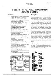
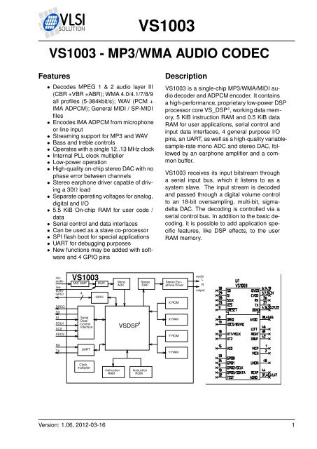
<strong>VS1003</strong>8 FUNCTIONAL DESCRIPTION8 Functional Description8.1 Main Features<strong>VS1003</strong> is based on a proprietary digital signal processor, VS_DSP. It contains all the codeand data memory needed for MP3, WMA and WAV PCM + ADPCM audio decoding, MIDIsynthesizer, together with serial interfaces, a multirate stereo audio DAC and analog outputamplifiers and filters. Also ADPCM audio encoding is supported using a microphone amplifierand A/D converter. A UART is provided for debugging purposes.8.2 Supported Audio CodecsMarkConventionsDescription+ Format is supported- Format exists but is not supportedFormat doesn’t exist8.2.1 Supported MP3 (MPEG layer III) FormatsMPEG 1.0 1 :Samplerate / HzBitrate / kbit/s32 40 48 56 64 80 96 112 128 160 192 224 256 32048000 + + + + + + + + + + + + + +44100 + + + + + + + + + + + + + +32000 + + + + + + + + + + + + + +MPEG 2.0 1 :Samplerate / HzBitrate / kbit/s8 16 24 32 40 48 56 64 80 96 112 128 144 16024000 + + + + + + + + + + + + + +22050 + + + + + + + + + + + + + +16000 + + + + + + + + + + + + + +MPEG 2.5 1 2 :Samplerate / HzBitrate / kbit/s8 16 24 32 40 48 56 64 80 96 112 128 144 16012000 + + + + + + + + + + + + + +11025 + + + + + + + + + + + + + +8000 + + + + + + + + + + + + + +1 Also all variable bitrate (VBR) formats are supported.2 Incompatibilities may occur because MPEG 2.5 is not a standard format.Version: 1.06, 2012-03-16 23
<strong>VS1003</strong>8 FUNCTIONAL DESCRIPTION8.2.2 Supported WMA FormatsWindows Media Audio codec versions 2, 7, 8, and 9 are supported. All WMA profiles (L1, L2,and L3) are supported. Previously streams were separated into Classes 1, 2a, 2b, and 3. WMA9 Professional and WMA 9 Lossless are not supported. The decoder has passed Microsoft’sconformance testing program.WMA 4.0 / 4.1:SamplerateBitrate / kbit/s/ Hz 5 6 8 10 12 16 20 22 32 40 48 64 80 96 128 160 192WMA 7:8000 + + + +11025 + +16000 + + + +22050 + + + +32000 + + + + + +44100 + + + + + + +48000 + +SamplerateBitrate / kbit/s/ Hz 5 6 8 10 12 16 20 22 32 40 48 64 80 96 128 160 192WMA 8:8000 + + + +11025 + +16000 + + + +22050 + + + +32000 + + + +44100 + + + + + + + +48000 + +SamplerateBitrate / kbit/s/ Hz 5 6 8 10 12 16 20 22 32 40 48 64 80 96 128 160 192WMA 9:8000 + + + +11025 + +16000 + + + +22050 + + + +32000 + + + +44100 + + + + + + + +48000 + + +SamplerateBitrate / kbit/s/ Hz 5 6 8 10 12 16 20 22 32 40 48 64 80 96 128 160 192 256 3208000 + + + +11025 + +16000 + + + +22050 + + + +32000 + + + +44100 + + + + + + + + + + +48000 + + + + +In addition to these expected WMA decoding profiles, all other bitrate and samplerate combinationsare supported, including variable bitrate WMA streams. Note that WMA does notconsume the bitstream as evenly as MP3, so you need a higher peak transfer capability forclean playback at the same bitrate.Version: 1.06, 2012-03-16 24
<strong>VS1003</strong>8 FUNCTIONAL DESCRIPTION8.2.3 Supported RIFF WAV FormatsThe most common RIFF WAV subformats are supported.Format Name Supported Comments0x01 PCM + 16 and 8 bits, any sample rate ≤ 48kHz0x02 ADPCM -0x03 IEEE_FLOAT -0x06 ALAW -0x07 MULAW -0x10 OKI_ADPCM -0x11 IMA_ADPCM + Any sample rate ≤ 48kHz0x15 DIGISTD -0x16 DIGIFIX -0x30 DOLBY_AC2 -0x31 GSM610 -0x3b ROCKWELL_ADPCM -0x3c ROCKWELL_DIGITALK -0x40 G721_ADPCM -0x41 G728_CELP -0x50 MPEG -0x55 MPEGLAYER3 + For supported MP3 modes, see Chapter 8.2.10x64 G726_ADPCM -0x65 G722_ADPCM -Version: 1.06, 2012-03-16 25
<strong>VS1003</strong>8 FUNCTIONAL DESCRIPTION8.2.4 Supported MIDI FormatsGeneral MIDI and SP-MIDI format 0 files are played. Format 1 and 2 files must be converted toformat 0 by the user. The maximum simultaneous polyphony is 40. Actual polyphony dependson the internal clock rate (which is user-selectable), the instruments used, and the possiblepostprocessing effects enabled, such as bass and treble enhancers. The polyphony restrictionalgorithm makes use of the SP-MIDI MIP table, if present.36.86 MHz (3.0× input clock) achieves 16-26 simultaneous sustained notes. The instantaneousamount of notes can be larger. 36 MHz is a fair compromise between power consumption andquality, but higher clocks can be used to increase polyphony.<strong>VS1003</strong>b implements 36 distinct instruments. Each melodic, effect, and percussion instrumentis mapped into one of these instruments.<strong>VS1003</strong>bMelodic Effect Percussionpiano reverse cymbal bass drumvibraphone guitar fret noise snareorgan breath closed hihatguitar seashore open hihatdistortion guitar bird tweet high tombass telephone low tomviolin helicopter crash cymbal 2strings applause ride cymbaltrumpet gunshot tambourinesaxhigh congaflutelow congaleadmaracaspadclavessteeldrumVersion: 1.06, 2012-03-16 26
<strong>VS1003</strong>8 FUNCTIONAL DESCRIPTION8.3 Data Flow of <strong>VS1003</strong>SDIBitstreamFIFOMP3/PlusV/WAV/ADPCM/WMA decode/MIDI decodeSM_ADPCM=0AIADDR = 0SB_AMPLITUDE=0ST_AMPLITUDE=0UserApplicationBassenhancerTrebleenhancerVolumecontrolAudioFIFOS.rate.conv.and DACLRAIADDR != 0SB_AMPLITUDE!=0ST_AMPLITUDE!=0SCI_VOL2048 stereosamplesFigure 16: Data Flow of <strong>VS1003</strong>.First, depending on the audio data, and provided ADPCM encoding mode is not set, MP3,WMA, PCM WAV, IMA ADPCM WAV, or MIDI data is received and decoded from the SDI bus.After decoding, if SCI_AIADDR is non-zero, application code is executed from the addresspointed to by that register. For more details, see Application Notes for VS10XX.Then data may be sent to the Bass and Treble Enhancer depending on the SCI_BASS register.After that the signal is fed to the volume control unit, which also copies the data to the AudioFIFO.The Audio FIFO holds the data, which is read by the Audio interrupt (Chapter 10.13.1) and fedto the sample rate converter and DACs. The size of the audio FIFO is 2048 stereo (2×16-bit)samples, or 8 KiB.The sample rate converter converts all different sample rates to XTALI/2, or 128 times thehighest usable sample rate. This removes the need for complex PLL-based clocking schemesand allows almost unlimited sample rate accuracy with one fixed input clock frequency. Witha 12.288 MHz clock, the DA converter operates at 128 × 48 kHz, i.e. 6.144 MHz, and createsa stereo in-phase analog signal. The oversampled output is low-pass filtered by an on-chipanalog filter. This signal is then forwarded to the earphone amplifier.8.4 Serial Data Interface (SDI)The serial data interface is meant for transferring compressed MP3 or WMA data, WAV PCMand ADPCM data as well as MIDI data.If the input of the decoder is invalid or it is not received fast enough, analog outputs are automaticallymuted.Also several different tests may be activated through SDI as described in Chapter 9.Version: 1.06, 2012-03-16 27
<strong>VS1003</strong>8 FUNCTIONAL DESCRIPTION8.5 Serial Control Interface (SCI)The serial control interface is compatible with the SPI bus specification. Data transfers arealways 16 bits. <strong>VS1003</strong> is controlled by writing and reading the registers of the interface.The main controls of the control interface are:• control of the operation mode, clock, and builtin effects• access to status information and header data• access to encoded digital data• uploading user programs8.6 SCI RegistersSCI registers, prefix SCI_Reg Type Reset Time 1 Abbrev[bits] Description0x0 rw 0x800 70 CLKI 4 MODE Mode control0x1 rw 0x3C 3 40 CLKI STATUS Status of <strong>VS1003</strong>0x2 rw 0 2100 CLKI BASS Built-in bass/treble enhancer0x3 rw 0 11000 XTALI 5 CLOCKF Clock freq + multiplier0x4 rw 0 40 CLKI DECODE_TIME Decode time in seconds0x5 rw 0 3200 CLKI AUDATA Misc. audio data0x6 rw 0 80 CLKI WRAM RAM write/read0x7 rw 0 80 CLKI WRAMADDR Base address for RAMwrite/read0x8 r 0 - HDAT0 Stream header data 00x9 r 0 - HDAT1 Stream header data 10xA rw 0 3200 CLKI 2 AIADDR Start address of application0xB rw 0 2100 CLKI VOL Volume control0xC rw 0 50 CLKI 2 AICTRL0 Application control register 00xD rw 0 50 CLKI 2 AICTRL1 Application control register 10xE rw 0 50 CLKI 2 AICTRL2 Application control register 20xF rw 0 50 CLKI 2 AICTRL3 Application control register 31 This is the worst-case time that DREQ stays low after writing to this register. The user maychoose to skip the DREQ check for those register writes that take less than 100 clock cycles toexecute.2 In addition, the cycles spent in the user application routine must be counted.3 Firmware changes the value of this register immediately to 0x38, and in less than 100 ms to0x30.4 When mode register write specifies a software reset the worst-case time is 16600 XTALIcycles.5 Writing to this register may force internal clock to run at 1.0 × XTALI for a while. Thus it is nota good idea to send SCI or SDI bits while this register update is in progress.Note that if DREQ is low when an SCI write is done, DREQ also stays low after SCI writeprocessing.Version: 1.06, 2012-03-16 28
<strong>VS1003</strong>8 FUNCTIONAL DESCRIPTION8.6.1 SCI_MODE (RW)SCI_MODE is used to control the operation of <strong>VS1003</strong> and defaults to 0x0800 (SM_SDINEWset).Bit Name Function Value Description0 SM_DIFF Differential 0 normal in-phase audio1 left channel inverted1 SM_SETTOZERO Set to zero 0 right1 wrong2 SM_RESET Soft reset 0 no reset1 reset3 SM_OUTOFWAV Jump out of WAV decoding 0 no1 yes4 SM_PDOWN Powerdown 0 power on1 powerdown5 SM_TESTS Allow SDI tests 0 not allowed1 allowed6 SM_STREAM Stream mode 0 no1 yes7 SM_SETTOZERO2 Set to zero 0 right1 wrong8 SM_DACT DCLK active edge 0 rising1 falling9 SM_SDIORD SDI bit order 0 MSb first1 MSb last10 SM_SDISHARE Share SPI chip select 0 no1 yes11 SM_SDINEW VS1002 native SPI modes 0 no1 yes12 SM_ADPCM ADPCM recording active 0 no1 yes13 SM_ADPCM_HP ADPCM high-pass filter active 0 no1 yes14 SM_LINE_IN ADPCM recording selector 0 microphone1 line inWhen SM_DIFF is set, the player inverts the left channel output. For a stereo input this createsvirtual surround, and for a mono input this creates a differential left/right signal.Software reset is initiated by setting SM_RESET to 1. This bit is cleared automatically.If you want to stop decoding a WAV, WMA, or MIDI file in the middle, set SM_OUTOFWAV, andsend data honouring DREQ until SM_OUTOFWAV is cleared. SCI_HDAT1 will also be cleared.For WMA and MIDI it is safest to continue sending the stream, send zeroes for WAV.Bit SM_PDOWN sets <strong>VS1003</strong> into software powerdown mode. Note that software powerdownis not nearly as power efficient as hardware powerdown activated with the XRESET pin.If SM_TESTS is set, SDI tests are allowed. For more details on SDI tests, look at Chapter 9.8.Version: 1.06, 2012-03-16 29
<strong>VS1003</strong>8 FUNCTIONAL DESCRIPTIONSM_STREAM activates <strong>VS1003</strong>’s stream mode. In this mode, data should be sent with aseven intervals as possible (and preferable with data blocks of less than 512 bytes), and <strong>VS1003</strong>makes every attempt to keep its input buffer half full by changing its playback speed upto 5%.For best quality sound, the average speed error should be within 0.5%, the bitrate should notexceed 160 kbit/s and VBR should not be used. For details, see Application Notes for VS10XX.This mode does not work with WMA files.SM_DACT defines the active edge of data clock for SDI. When ’0’, data is read at the risingedge, when ’1’, data is read at the falling edge.When SM_SDIORD is clear, bytes on SDI are sent as a default MSb first. By setting SM_SDIORD,the user may reverse the bit order for SDI, i.e. bit 0 is received first and bit 7 last. Bytes are,however, still sent in the default order. This register bit has no effect on the SCI bus.Setting SM_SDISHARE makes SCI and SDI share the same chip select, as explained in Chapter7.2, if also SM_SDINEW is set.Setting SM_SDINEW will activate VS1002 native serial modes as described in Chapters 7.2.1 and 7.4.2.Note, that this bit is set as a default when <strong>VS1003</strong> is started up.By activating SM_ADPCM and SM_RESET at the same time, the user will activate IMA ADPCMrecording mode. More information is available in the Application Notes for VS10XX.If SM_ADPCM_HP is set at the same time as SM_ADPCM and SM_RESET, ADPCM modewill start with a high-pass filter. This may help intelligibility of speech when there is lots ofbackground noise. The difference created to the ADPCM encoder frequency response is asshown in Figure 17.5<strong>VS1003</strong> AD Converter with and Without HP FilterNo High−PassHigh−Pass0Amplitude / dB−5−10−15−200 500 1000 1500 2000 2500 3000 3500 4000Frequency / HzFigure 17: ADPCM Frequency Responses with 8kHz sample rate.SM_LINE_IN is used to select the input for ADPCM recording. If ’0’, microphone input pinsMICP and MICN are used; if ’1’, LINEIN is used.Version: 1.06, 2012-03-16 30
<strong>VS1003</strong>8 FUNCTIONAL DESCRIPTION8.6.2 SCI_STATUS (RW)SCI_STATUS contains information on the current status of <strong>VS1003</strong> and lets the user shutdownthe chip without audio glitches.Name Bits DescriptionSS_VER 6:4 VersionSS_APDOWN2 3 Analog driver powerdownSS_APDOWN1 2 Analog internal powerdownSS_AVOL 1:0 Analog volume controlSS_VER is 0 for VS1001, 1 for VS1011, 2 for VS1002 and 3 for <strong>VS1003</strong>.SS_APDOWN2 controls analog driver powerdown. Normally this bit is controlled by the systemfirmware. However, if the user wants to powerdown <strong>VS1003</strong> with a minimum power-offtransient, turn this bit to 1, then wait for at least a few milliseconds before activating reset.SS_APDOWN1 controls internal analog powerdown. This bit is meant to be used by the systemfirmware only.SS_AVOL is the analog volume control: 0 = -0 dB, 1 = -6 dB, 3 = -12 dB. This register is meantto be used automatically by the system firmware only.8.6.3 SCI_BASS (RW)Name Bits DescriptionST_AMPLITUDE 15:12 Treble Control in 1.5 dB steps (-8..7, 0 = off)ST_FREQLIMIT 11:8 Lower limit frequency in 1000 Hz steps (0..15)SB_AMPLITUDE 7:4 Bass Enhancement in 1 dB steps (0..15, 0 = off)SB_FREQLIMIT 3:0 Lower limit frequency in 10 Hz steps (2..15)The Bass Enhancer VSBE is a powerful bass boosting DSP algorithm, which tries to take themost out of the users earphones without causing clipping.VSBE is activated when SB_AMPLITUDE is non-zero. SB_AMPLITUDE should be set to theuser’s preferences, and SB_FREQLIMIT to roughly 1.5 times the lowest frequency the user’saudio system can reproduce. For example setting SCI_BASS to 0x00f6 will have 15 dB enhancementbelow 60 Hz.Note: Because VSBE tries to avoid clipping, it gives the best bass boost with dynamical musicmaterial, or when the playback volume is not set to maximum. It also does not create bass: thesource material must have some bass to begin with.Treble Control VSTC is activated when ST_AMPLITUDE is non-zero. For example settingSCI_BASS to 0x7a00 will have 10.5 dB treble enhancement at and above 10 kHz.Bass Enhancer uses about 3.0 MIPS and Treble Control 1.2 MIPS at 44100 Hz sample rate.Both can be on simultaneously.Version: 1.06, 2012-03-16 31
<strong>VS1003</strong>8 FUNCTIONAL DESCRIPTION8.6.4 SCI_CLOCKF (RW)The operation of SCI_CLOCKF is different in <strong>VS1003</strong> than in VS10x1 and VS1002.SCI_CLOCKF bitsName Bits DescriptionSC_MULT 15:13 Clock multiplierSC_ADD 12:11 Allowed multiplier additionSC_FREQ 10: 0 Clock frequencySC_MULT activates the built-in clock multiplier. This will multiply XTALI to create a higher CLKI.The values are as follows:SC_MULT MASK CLKI0 0x0000 XTALI1 0x2000 XTALI×1.52 0x4000 XTALI×2.03 0x6000 XTALI×2.54 0x8000 XTALI×3.05 0xa000 XTALI×3.56 0xc000 XTALI×4.07 0xe000 XTALI×4.5SC_ADD tells, how much the decoder firmware is allowed to add to the multiplier specified bySC_MULT if more cycles are temporarily needed to decode a WMA stream. The values are:SC_ADD MASK Multiplier addition0 0x0000 No modification is allowed1 0x0800 0.5×2 0x1000 1.0×3 0x1800 1.5×SC_FREQ is used to tell if the input clock XTALI is running at something else than 12.288 MHz.XTALI is set in 4 kHz steps. The formula for calculating the correct value for this register isXT ALI−80000004000(XTALI is in Hz).Note: The default value 0 is assumed to mean XTALI=12.288 MHz.Note: because maximum sample rate is< 12.288 MHz.XT ALI256, all sample rates are not available if XTALINote: Automatic clock change can only happen when decoding WMA files. Automatic clockchange is done one 0.5× at a time. This does not cause a drop to 1.0× clock and you canuse the same SCI and SDI clock throughout the WMA file. When decoding ends the defaultmultiplier is restored and can cause 1.0× clock to be used momentarily.Example: If SCI_CLOCKF is 0x9BE8, SC_MULT = 4, SC_ADD = 3 and SC_FREQ = 0x3E8 = 1000.This means that XTALI = 1000 × 4000 + 8000000 = 12 MHz. The clock multiplier is set to3.0×XTALI = 36 MHz, and the maximum allowed multiplier that the firmware may automaticallychoose to use is (3.0 + 1.5)×XTALI = 54 MHz.Version: 1.06, 2012-03-16 32
<strong>VS1003</strong>8 FUNCTIONAL DESCRIPTION8.6.5 SCI_DECODE_TIME (RW)When decoding correct data, current decoded time is shown in this register in full seconds.The user may change the value of this register. In that case the new value should be writtentwice.SCI_DECODE_TIME is reset at every software reset and also when WAV (PCM or IMA AD-PCM), WMA, or MIDI decoding starts or ends.8.6.6 SCI_AUDATA (RW)When decoding correct data, the current sample rate and number of channels can be found inbits 15:1 and 0 of SCI_AUDATA, respectively. Bits 15:1 contain the sample rate divided by two,and bit 0 is 0 for mono data and 1 for stereo. Writing to SCI_AUDATA will change the samplerate directly.Note: due to a bug, an odd sample rate reverses the operation of the stereo bit in <strong>VS1003</strong>b.Example: 44100 Hz stereo data reads as 0xAC45 (44101).Example: 11025 Hz mono data reads as 0x2B10 (11025).Example: 11025 Hz stereo data reads as 0x2B11 (11026).Example: Writing 0xAC80 sets sample rate to 44160 Hz, stereo mode does not change.8.6.7 SCI_WRAM (RW)SCI_WRAM is used to upload application programs and data to instruction and data RAMs.The start address must be initialized by writing to SCI_WRAMADDR prior to the first write/readof SCI_WRAM. As 16 bits of data can be transferred with one SCI_WRAM write/read, and theinstruction word is 32 bits long, two consecutive writes/reads are needed for each instructionword. The byte order is big-endian (i.e. most significant words first). After each full-wordwrite/read, the internal pointer is autoincremented.8.6.8 SCI_WRAMADDR (W)SCI_WRAMADDR is used to set the program address for following SCI_WRAM writes/reads.Address offset of 0 is used for X, 0x4000 for Y, and 0x8000 for instruction memory. Peripheralregisters can also be accessed.SM_WRAMADDR Dest. addr. Bits/ DescriptionStart. . . End Start. . . End Word0x1800. . . 0x187F 0x1800. . . 0x187F 16 X data RAM0x5800. . . 0x587F 0x1800. . . 0x187F 16 Y data RAM0x8030. . . 0x84FF 0x0030. . . 0x04FF 32 Instruction RAM0xC000. . . 0xFFFF 0xC000. . . 0xFFFF 16 I/OOnly user areas in X, Y, and instruction memory are listed above. Other areas can be accessed,but should not be written to unless otherwise specified.Version: 1.06, 2012-03-16 33
<strong>VS1003</strong>8 FUNCTIONAL DESCRIPTION8.6.9 SCI_HDAT0 and SCI_HDAT1 (R)For WAV files, SCI_HDAT0 and SCI_HDAT1 read as 0x7761, and 0x7665, respectively.For WMA files, SCI_HDAT1 contains 0x574D and SCI_HDAT0 contains the data speed measuredin bytes per second. To get the bit-rate of the file, multiply the value of SCI_HDAT0 by8.for MIDI files, SCI_HDAT1 contains 0x4D54 and SCI_HDAT0 contains values according to thefollowing table:HDAT0[15:8] HDAT0[7:0] Value Explanation0 polyphony current polyphony1..255 reservedFor MP3 files, SCI_HDAT[0. . . 1] have the following content:Bit Function Value ExplanationHDAT1[15:5] syncword 2047 stream validHDAT1[4:3] ID 3 ISO 11172-3 MPG 1.02 ISO 13818-3 MPG 2.0 (1/2-rate)1 MPG 2.5 (1/4-rate)0 MPG 2.5 (1/4-rate)HDAT1[2:1] layer 3 I2 II1 III0 reservedHDAT1[0] protect bit 1 No CRC0 CRC protectedHDAT0[15:12] bitrate ISO 11172-3HDAT0[11:10] sample rate 3 reserved2 32/16/ 8 kHz1 48/24/12 kHz0 44/22/11 kHzHDAT0[9] pad bit 1 additional slot0 normal frameHDAT0[8] private bit not definedHDAT0[7:6] mode 3 mono2 dual channel1 joint stereo0 stereoHDAT0[5:4] extension ISO 11172-3HDAT0[3] copyright 1 copyrighted0 freeHDAT0[2] original 1 original0 copyHDAT0[1:0] emphasis 3 CCITT J.172 reserved1 50/15 microsec0 noneVersion: 1.06, 2012-03-16 34
<strong>VS1003</strong>8 FUNCTIONAL DESCRIPTIONWhen read, SCI_HDAT0 and SCI_HDAT1 contain header information that is extracted fromMP3 stream currently being decoded. After reset both registers are cleared, indicating no datahas been found yet.The “sample rate” field in SCI_HDAT0 is interpreted according to the following table:“sample rate” ID=3 / Hz ID=2 / Hz ID=0,1 / Hz3 - - -2 32000 16000 80001 48000 24000 120000 44100 22050 11025The “bitrate” field in HDAT0 is read according to the following table:“bitrate” ID=3 / kbit/s ID=0,1,2 / kbit/s15 forbidden forbidden14 320 16013 256 14412 224 12811 192 11210 160 969 128 808 112 647 96 566 80 485 64 404 56 323 48 242 40 161 32 80 - -8.6.10 SCI_AIADDR (RW)SCI_AIADDR indicates the start address of the application code written earlier with SCI_WRAMADDRand SCI_WRAM registers. If no application code is used, this register should not be initialized,or it should be initialized to zero. For more details, see Application Notes for VS10XX.Version: 1.06, 2012-03-16 35
<strong>VS1003</strong>8 FUNCTIONAL DESCRIPTION8.6.11 SCI_VOL (RW)SCI_VOL is a volume control for the player hardware. For each channel, a value in the range of0..254 may be defined to set its attenuation from the maximum volume level (in 0.5 dB steps).The left channel value is then multiplied by 256 and the values are added. Thus, maximumvolume is 0 and total silence is 0xFEFE.Example: for a volume of -2.0 dB for the left channel and -3.5 dB for the right channel: (4*256)+ 7 = 0x407. Note, that at startup volume is set to full volume. Resetting the software does notreset the volume setting.Note: Setting SCI_VOL to 0xFFFF will activate analog powerdown mode.8.6.12 SCI_AICTRL[x] (RW)SCI_AICTRL[x] registers ( x=[0 .. 3] ) can be used to access the user’s application program.Version: 1.06, 2012-03-16 36
<strong>VS1003</strong>9 OPERATION9 Operation9.1 Clocking<strong>VS1003</strong> operates on a single, nominally 12.288 MHz fundamental frequency master clock. Thisclock can be generated by external circuitry (connected to pin XTALI) or by the internal clockcrystal interface (pins XTALI and XTALO).9.2 Hardware ResetWhen the XRESET -signal is driven low, <strong>VS1003</strong> is reset and all the control registers andinternal states are set to the initial values. XRESET-signal is asynchronous to any externalclock. The reset mode doubles as a full-powerdown mode, where both digital and analog partsof <strong>VS1003</strong> are in minimum power consumption stage, and where clocks are stopped. AlsoXTALO is grounded.After a hardware reset (or at power-up) DREQ will stay down for at least 16600 clock cycles,which means an approximate 1.35 ms delay if <strong>VS1003</strong> is run at 12.288 MHz. After this theuser should set such basic software registers as SCI_MODE, SCI_BASS, SCI_CLOCKF, andSCI_VOL before starting decoding. See section 8.6 for details.Internal clock can be multiplied with a PLL. Supported multipliers through the SCI_CLOCKFregister are 1.0 × . . . 4.5× the input clock. Reset value for Internal Clock Multiplier is 1.0×. Iftypical values are wanted, the Internal Clock Multiplier needs to be set to 3.0× after reset. Waituntil DREQ rises, then write value 0x9800 to SCI_CLOCKF (register 3). See section 8.6.4 fordetails.9.3 Software ResetIn some cases the decoder software has to be reset. This is done by activating bit 2 inSCI_MODE register (Chapter 8.6.1). Then wait for at least 2 µs, then look at DREQ. DREQwill stay down for at least 16600 clock cycles, which means an approximate 1.35 ms delay if<strong>VS1003</strong> is run at 12.288 MHz. After DREQ is up, you may continue playback as usual.If you want to make sure <strong>VS1003</strong> doesn’t cut the ending of low-bitrate data streams and youwant to do a software reset, it is recommended to feed 2048 zeros (honoring DREQ) to the SDIbus after the file and before the reset. This is especially important for MIDI files, although youcan also use SCI_HDAT1 polling.If you want to interrupt the playing of a WAV, WMA, or MIDI file in the middle, set SM_OUTOFWAVin the mode register, and wait until SCI_HDAT1 is cleared (with a two-second timeout) beforecontinuing with a software reset. MP3 does not currently implement the SM_OUTOFWAV becauseit is a stream format, thus the timeout requirement.Version: 1.06, 2012-03-16 37
<strong>VS1003</strong>9 OPERATION9.4 ADPCM RecordingThis chapter explains how to create RIFF/WAV file with IMA ADPCM format. This is a widelysupported ADPCM format and many PC audio playback programs can play it. IMA ADPCMrecording gives roughly a compression ratio of 4:1 compared to linear, 16-bit audio. This makesit possible to record 8 kHz audio at 32.44 kbit/s.9.4.1 Activating ADPCM modeIMA ADPCM recording mode is activated by setting bits SM_RESET and SM_ADPCM inSCI_MODE. Optionally a high-pass-filter can be enabled for 8 kHz sample rate by also settingSM_ADPCM_HP at the same time. Line input is used instead of mic if SM_LINE_IN is set.Before activating ADPCM recording, user must write a clock divider value to SCI_AICTRL0and gain to SCI_AICTRL1.The differences of using SM_ADPCM_HP are presented in figure 17 (page 30). As a generalrule, audio will be fuller and closer to original if SM_ADPCM_HP is not used. However, speechmay be more intelligible with the high-pass filter active. Use the filter only with 8 kHz samplerate.Before activating ADPCM recording, user should write a clock divider value to SCI_AICTRL0.The sampling frequency is calculated from the following formula: f s =Fc256×d , where F c is theinternal clock (CLKI) and d is the divider value in SCI_AICTRL0. The lowest valid value for d is4. If SCI_AICTRL0 contains 0, the default divider value 12 is used.Examples:F c = 2.0 × 12.288 MHz, d = 12. Now f s = 2.0×12288000256×12= 8000 Hz.F c = 2.5 × 14.745 MHz, d = 18. Now f s = 2.5×14745000256×18= 8000 Hz.F c = 2.5 × 13 MHz, d = 16. Now f s = 2.5×13000000256×16= 7935 Hz.Also, before activating ADPCM mode, the user has to set linear recording gain control to registerSCI_AICTRL1. 1024 is equal to digital gain 1, 512 is equal to digital gain 0.5 and so on. If theuser wants to use automatic gain control (AGC), SCI_AICTRL1 should be set to 0. Typicalspeech applications usually are better off using AGC, as this takes care of relatively uniformspeech loudness in recordings.Since VS1033c SCI_AICTRL2 controls the maximum AGC gain. If SCI_AICTRL2 is zero, themaximum gain is 65535 (64×), i.e. whole range is used. This is compatible with previousoperation.9.4.2 Reading IMA ADPCM DataAfter IMA ADPCM recording has been activated, registers SCI_HDAT0 and SCI_HDAT1 havenew functions.The IMA ADPCM sample buffer is 1024 16-bit words. The fill status of the buffer can be readfrom SCI_HDAT1. If SCI_HDAT1 is greater than 0, you can read as many 16-bit words fromSCI_HDAT0. If the data is not read fast enough, the buffer overflows and returns to empty state.Version: 1.06, 2012-03-16 38
<strong>VS1003</strong>9 OPERATIONNote: if SCI_HDAT1 ≥ 896, it may be better to wait for the buffer to overflow and clear beforereading samples. That way you may avoid buffer aliasing.Each IMA ADPCM block is 128 words, i.e. 256 bytes. If you wish to interrupt reading dataand possibly continue later, please stop at a 128-word boundary. This way whole blocks areskipped and the encoded stream stays valid.9.4.3 Adding a RIFF HeaderTo make your IMA ADPCM file a RIFF / WAV file, you have to add a header before the actualdata. Note that 2- and 4-byte values are little-endian (lowest byte first) in this format:File Offset Field Name Size Bytes Description0 ChunkID 4 "RIFF"4 ChunkSize 4 F0 F1 F2 F3 File size - 88 Format 4 "WAVE"12 SubChunk1ID 4 "fmt "16 SubChunk1Size 4 0x14 0x0 0x0 0x0 2020 AudioFormat 2 0x11 0x0 0x11 for IMA ADPCM22 NumOfChannels 2 0x1 0x0 Mono sound24 SampleRate 4 R0 R1 R2 R3 0x1f40 for 8 kHz28 ByteRate 4 B0 B1 B2 B3 0xfd7 for 8 kHz32 BlockAlign 2 0x0 0x1 0x10034 BitsPerSample 2 0x4 0x0 4-bit ADPCM36 ByteExtraData 2 0x2 0x0 238 ExtraData 2 0xf9 0x1 Samples per block (505)40 SubChunk2ID 4 "fact"44 SubChunk2Size 4 0x4 0x0 0x0 0x0 448 NumOfSamples 4 S0 S1 S2 S352 SubChunk3ID 4 "data"56 SubChunk3Size 4 D0 D1 D2 D3 Data size (File Size-60)60 Block1 256 First ADPCM block316 . . . More ADPCM data blocksIf we have n audio blocks, the values in the table are as follows:F = n × 256 + 52R = F s (see Chapter 9.4.1 to see how to calculate F s )B = Fs×256505S = n × 505. D = n × 256If you know beforehand how much you are going to record, you may fill in the complete headerbefore any actual data. However, if you don’t know how much you are going to record, you haveto fill in the header size datas F , S and D after finishing recording.The 128 words (256 bytes) of an ADPCM block are read from SCI_HDAT0 and written into fileas follows. The high 8 bits of SCI_HDAT0 should be written as the first byte to a file, then thelow 8 bits. Note that this is contrary to the default operation of some 16-bit microcontrollers,and you may have to take extra care to do this right.Version: 1.06, 2012-03-16 39
<strong>VS1003</strong>9 OPERATIONA way to see if you have written the file in the right way is to check bytes 2 and 3 (the first bytecounts as byte 0) of each 256-byte block. Byte 3 should always be zero.9.4.4 Playing ADPCM DataIn order to play back your IMA ADPCM recordings, you have to have a file with a header asdescribed in Chapter 9.4.3. If this is the case, all you need to do is to provide the ADPCM filethrough SDI as you would with any audio file.9.4.5 Sample Rate ConsiderationsVS10xx chips that support IMA ADPCM playback are capable of playing back ADPCM files withany sample rate. However, some other programs may expect IMA ADPCM files to have someexact sample rates, like 8000 or 11025 Hz. Also, some programs or systems do not supportsample rates below 8000 Hz.However, if you don’t have an appropriate clock, you may not be able to get an exact 8 kHzsample rate. If you have a 12 MHz clock, the closest sample rate you can get with 2.0 × 12 MHzand d = 12 is f s = 7812.5Hz. Because the frequency error is only 2.4%, it may be best to setf s = 8000Hz to the header if the same file is also to be played back with an PC. This causesthe sample to be played back a little faster (one minute is played in 59 seconds).Note, however, that unless absolutely necessary, sample rates should not be tweaked in theway described here.If you want better quality with the expense of increased data rate, you can use higher samplerates, for example 16 kHz.9.4.6 Example CodeThe following code initializes IMA ADPCM encoding on <strong>VS1003</strong>b/VS1023 and shows how toread the data.const unsigned char header[] = {0x52, 0x49, 0x46, 0x46, 0x1c, 0x10, 0x00, 0x00,0x57, 0x41, 0x56, 0x45, 0x66, 0x6d, 0x74, 0x20, /*|RIFF....WAVEfmt |*/0x14, 0x00, 0x00, 0x00, 0x11, 0x00, 0x01, 0x00,0x40, 0x1f, 0x00, 0x00, 0x75, 0x12, 0x00, 0x00, /*|........@...×...|*/0x00, 0x01, 0x04, 0x00, 0x02, 0x00, 0xf9, 0x01,0x66, 0x61, 0x63, 0x74, 0x04, 0x00, 0x00, 0x00, /*|......ù.fact....|*/0x5c, 0x1f, 0x00, 0x00, 0x64, 0x61, 0x74, 0x61,0xe8, 0x0f, 0x00, 0x00};unsigned char db[512]; /* data buffer for saving to disk */Version: 1.06, 2012-03-16 40
<strong>VS1003</strong>9 OPERATIONvoid RecordAdpcm1003(void) { /* <strong>VS1003</strong>b/VS1033c */u_int16 w = 0, idx = 0;}... /* Check and locate free space on disk */SetMp3Vol(0x1414); /* Recording monitor volume */WriteMp3SpiReg(SCI_BASS, 0); /* Bass/treble disabled */WriteMp3SpiReg(SCI_CLOCKF, 0x4430); /* 2.0x 12.288MHz */Wait(100);WriteMp3SpiReg(SCI_AICTRL0, 12); /* Div -> 12=8kHz 8=12kHz 6=16kHz */Wait(100);WriteMp3SpiReg(SCI_AICTRL1, 0); /* Auto gain */Wait(100);if (line_in) {WriteMp3SpiReg(SCI_MODE, 0x5804); /* Normal SW reset + other bits */} else {WriteMp3SpiReg(SCI_MODE, 0x1804); /* Normal SW reset + other bits */}for (idx=0; idx < sizeof(header); idx++) { /* Save header first */db[idx] = header[idx];}/* Fix rate if needed *//*db[24] = rate;*//*db[25] = rate>>8;*//* Record loop */while (recording_on) {do {w = ReadMp3SpiReg(SCI_HDAT1);} while (w < 256 || w >= 896); /* wait until 512 bytes available */while (idx < 512) {w = ReadMp3SpiReg(SCI_HDAT0);db[idx++] = w>>8;db[idx++] = w&0xFF;}idx = 0;write_block(datasector++, db); /* Write output block to disk */}... /* Fix WAV header information */... /* Then update FAT information */ResetMP3(); /* Normal reset, restore default settings */SetMp3Vol(vol);Version: 1.06, 2012-03-16 41
<strong>VS1003</strong>9 OPERATION9.5 SPI BootIf GPIO0 is set with a pull-up resistor to 1 at boot time, <strong>VS1003</strong> tries to boot from external SPImemory.SPI boot redefines the following pins:Normal ModeGPIO0GPIO1DREQGPIO2SPI Boot ModexCSCLKMOSIMISOThe memory has to be an SPI Bus Serial EEPROM with 16-bit addresses (i.e. at least 1 KiB).The serial speed used by <strong>VS1003</strong> is 245 kHz with the nominal 12.288 MHz clock. The firstthree bytes in the memory have to be 0x50, 0x26, 0x48. The exact record format is explainedin the Application Notes for VS10XX.9.6 Play/DecodeThis is the normal operation mode of <strong>VS1003</strong>. SDI data is decoded. Decoded samples areconverted to analog domain by the internal DAC. If no decodable data is found, SCI_HDAT0and SCI_HDAT1 are set to 0 and analog outputs are muted.When there is no input for decoding, <strong>VS1003</strong> goes into idle mode (lower power consumptionthan during decoding) and actively monitors the serial data input for valid data.All different formats can be played back-to-back without software reset in-between. Send atleast 4 zeros after each stream. However, using software reset between streams may still be agood idea, as it guards against broken files. In this case you shouldt wait for the completion ofthe decoding (SCI_HDAT0 and SCI_HDAT1 become zero) before issuing software reset.9.7 Feeding PCM data<strong>VS1003</strong> can be used as a PCM decoder by sending to it a WAV file header. If the lengthsent in the WAV file is 0 or 0xFFFFFFF, <strong>VS1003</strong> will stay in PCM mode indefinitely (or untilSM_OUTOFWAV has been set). 8-bit linear and 16-bit linear audio is supported in mono orstereo.Version: 1.06, 2012-03-16 42
<strong>VS1003</strong>9 OPERATION9.8 SDI TestsThere are several test modes in <strong>VS1003</strong>, which allow the user to perform memory tests, SCIbus tests, and several different sine wave tests.All tests are started in a similar way: <strong>VS1003</strong> is hardware reset, SM_TESTS is set, and then atest command is sent to the SDI bus. Each test is started by sending a 4-byte special commandsequence, followed by 4 zeros. The sequences are described below.9.8.1 Sine TestSine test is initialized with the 8-byte sequence 0x53 0xEF 0x6E n 0 0 0 0, where n defines thesine test to use. n is defined as follows:n bitsName Bits DescriptionF s Idx 7:5 Sample rate indexS 4:0 Sine skip speedF s Idx F s0 44100 Hz1 48000 Hz2 32000 Hz3 22050 Hz4 24000 Hz5 16000 Hz6 11025 Hz7 12000 HzThe frequency of the sine to be output can now be calculated from F = F s × S128 .Example: Sine test is activated with value 126, which is 0b01111110. Breaking n to its components,F s Idx = 0b011 = 3 and thus F s = 22050Hz. S = 0b11110 = 30, and thus the final sinefrequency F = 22050Hz × 30128 ≈ 5168Hz.To exit the sine test, send the sequence 0x45 0x78 0x69 0x74 0 0 0 0.Note: Sine test signals go through the digital volume control, so it is possible to test channelsseparately.Version: 1.06, 2012-03-16 43
<strong>VS1003</strong>9 OPERATION9.8.2 Pin TestPin test is activated with the 8-byte sequence 0x50 0xED 0x6E 0x54 0 0 0 0. This test is meantfor chip production testing only.9.8.3 Memory TestMemory test mode is initialized with the 8-byte sequence 0x4D 0xEA 0x6D 0x54 0 0 0 0. Afterthis sequence, wait for 500000 clock cycles. The result can be read from the SCI registerSCI_HDAT0, and ’one’ bits are interpreted as follows:Bit(s) Mask Meaning15 0x8000 Test finished14:7 Unused6 0x0040 Mux test succeeded5 0x0020 Good I RAM4 0x0010 Good Y RAM3 0x0008 Good X RAM2 0x0004 Good I ROM1 0x0002 Good Y ROM0 0x0001 Good X ROM0x807fAll okMemory tests overwrite the current contents of the RAM memories.9.8.4 SCI TestSci test is initialized with the 8-byte sequence 0x53 0x70 0xEE n 0 0 0 0, where n is theregister number to test. The content of the given register is read and copied to SCI_HDAT0. Ifthe register to be tested is HDAT0, the result is copied to SCI_HDAT1.Example: if n is 0, contents of SCI register 0 (SCI_MODE) is copied to SCI_HDAT0.Version: 1.06, 2012-03-16 44
<strong>VS1003</strong>10 <strong>VS1003</strong> REGISTERS10 <strong>VS1003</strong> Registers10.1 Who Needs to Read This ChapterUser software is required when a user wishes to add some own functionality like DSP effectsto <strong>VS1003</strong>.However, most users of <strong>VS1003</strong> don’t need to worry about writing their own code, or about thischapter, including those who only download software plug-ins from <strong>VLSI</strong> <strong>Solution</strong>’s Web site.10.2 The Processor CoreVS_DSP is a 16/32-bit DSP processor core that also had extensive all-purpose processor features.<strong>VLSI</strong> <strong>Solution</strong>’s free VSKIT Software Package contains all the tools and documentationneeded to write, simulate and debug Assembly Language or Extended ANSI C programs for theVS_DSP processor core. <strong>VLSI</strong> <strong>Solution</strong> also offers a full Integrated Development EnvironmentVSIDE for full debug capabilities.10.3 <strong>VS1003</strong> Memory Map<strong>VS1003</strong>’s Memory Map is shown in Figure 18.10.4 SCI RegistersSCI registers described in Chapter 8.6 can be found here between 0xC000..0xC00F. In additionto these registers, there is one in address 0xC010, called SCI_CHANGE.SCI registers, prefix SCI_Reg Type Reset Abbrev[bits] Description0xC010 r 0 CHANGE[5:0] Last SCI access address.SCI_CHANGE bitsName Bits DescriptionSCI_CH_WRITE 4 1 if last access was a write cycle.SCI_CH_ADDR 3:0 SPI address of last access.Version: 1.06, 2012-03-16 45
<strong>VS1003</strong>10 <strong>VS1003</strong> REGISTERSInstruction (32−bit)X (16−bit)Y (16−bit)000000000030 System Vectors0030UserInstruction0500 RAM0500X DATAY DATARAMRAM18001880UserSpaceUserSpace180018801940StackStack19401C001C001E001E004000 4000InstructionROMX DATAROMY DATAROM8000 8000C000C100HardwareRegisterSpaceC000C100Figure 18: User’s Memory Map.10.5 Serial Data RegistersSDI registers, prefix SER_Reg Type Reset Abbrev[bits] Description0xC011 r 0 DATA Last received 2 bytes, big-endian.0xC012 w 0 DREQ[0] DREQ pin control.Version: 1.06, 2012-03-16 46
<strong>VS1003</strong>10 <strong>VS1003</strong> REGISTERS10.6 DAC RegistersDAC registers, prefix DAC_Reg Type Reset Abbrev[bits] Description0xC013 rw 0 FCTLL DAC frequency control, 16 LSbs.0xC014 rw 0 FCTLH DAC frequency control 4MSbs, PLL control.0xC015 rw 0 LEFT DAC left channel PCM value.0xC016 rw 0 RIGHT DAC right channel PCM value.Every fourth clock cycle, an internal 26-bit counter is added to by (DAC_FCTLH & 15) × 65536+ DAC_FCTLL. Whenever this counter overflows, values from DAC_LEFT and DAC_RIGHTare read and a DAC interrupt is generated.10.7 GPIO RegistersGPIO registers, prefix GPIO_Reg Type Reset Abbrev[bits] Description0xC017 rw 0 DDR[3:0] Direction.0xC018 r 0 IDATA[3:0] Values read from the pins.0xC019 rw 0 ODATA[3:0] Values set to the pins.GPIO_DIR is used to set the direction of the GPIO pins. 1 means output. GPIO_ODATAremembers its values even if a GPIO_DIR bit is set to input.GPIO registers don’t generate interrupts.Note that in <strong>VS1003</strong> the VSDSP registers can be read and written through the SCI_WRAMADDRand SCI_WRAM registers. You can thus use the GPIO pins quite conveniently.Version: 1.06, 2012-03-16 47
<strong>VS1003</strong>10 <strong>VS1003</strong> REGISTERS10.8 Interrupt RegistersInterrupt registers, prefix INT_Reg Type Reset Abbrev[bits] Description0xC01A rw 0 ENABLE[7:0] Interrupt enable.0xC01B w 0 GLOB_DIS[-] Write to add to interrupt counter.0xC01C w 0 GLOB_ENA[-] Write to subtract from interript counter.0xC01D rw 0 COUNTER[4:0] Interrupt counter.INT_ENABLE controls the interrupts. The control bits are as follows:INT_ENABLE bitsName Bits DescriptionINT_EN_TIM1 7 Enable Timer 1 interrupt.INT_EN_TIM0 6 Enable Timer 0 interrupt.INT_EN_RX 5 Enable UART RX interrupt.INT_EN_TX 4 Enable UART TX interrupt.INT_EN_MODU 3 Enable AD modulator interrupt.INT_EN_SDI 2 Enable Data interrupt.INT_EN_SCI 1 Enable SCI interrupt.INT_EN_DAC 0 Enable DAC interrupt.Note: It may take upto 6 clock cycles before changing INT_ENABLE has any effect.Writing any value to INT_GLOB_DIS adds one to the interrupt counter INT_COUNTER andeffectively disables all interrupts. It may take upto 6 clock cycles before writing to this registerhas any effect.Writing any value to INT_GLOB_ENA subtracts one from the interrupt counter (unless INT_COUNTERalready was 0). If the interrupt counter becomes zero, interrupts selected with INT_ENABLEare restored. An interrupt routine should always write to this register as the last thing it does,because interrupts automatically add one to the interrupt counter, but subtracting it back to itsinitial value is the responsibility of the user. It may take upto 6 clock cycles before writing thisregister has any effect.By reading INT_COUNTER the user may check if the interrupt counter is correct or not. If theregister is not 0, interrupts are disabled.Version: 1.06, 2012-03-16 48
<strong>VS1003</strong>10 <strong>VS1003</strong> REGISTERS10.9 A/D Modulator RegistersInterrupt registers, prefix AD_Reg Type Reset Abbrev[bits] Description0xC01E rw 0 DIV A/D Modulator divider.0xC01F rw 0 DATA A/D Modulator data.AD_DIV controls the AD converter’s sampling frequency. To gather one sample, 128 × n clockcycles are used (n is value of AD_DIV). The lowest usable value is 4, which gives a 48 kHzsample rate when CLKI is 24.576 MHz. When AD_DIV is 0, the A/D converter is turned off.AD_DATA contains the latest decoded A/D value.Version: 1.06, 2012-03-16 49
<strong>VS1003</strong>10 <strong>VS1003</strong> REGISTERS10.10 Watchdog v1.0 2002-08-26The watchdog consist of a watchdog counter and some logic. After reset, the watchdog isinactive. The counter reload value can be set by writing to WDOG_CONFIG. The watchdog isactivated by writing 0x4ea9 to register WDOG_RESET. Every time this is done, the watchdogcounter is reset. Every 65536’th clock cycle the counter is decremented by one. If the counterunderflows, it will activate vsdsp’s internal reset sequence.Thus, after the first 0x4ea9 write to WDOG_RESET, subsequent writes to the same registerwith the same value must be made no less than every 65536×WDOG_CONFIG clock cycles.Once started, the watchdog cannot be turned off. Also, a write to WDOG_CONFIG doesn’tchange the counter reload value.After watchdog has been activated, any read/write operation from/to WDOG_CONFIG or WDOG_DUMMYwill invalidate the next write operation to WDOG_RESET. This will prevent runaway loops fromresetting the counter, even if they do happen to write the correct number. Writing a wrong valueto WDOG_RESET will also invalidate the next write to WDOG_RESET.Reads from watchdog registers return undefined values.10.10.1 RegistersWatchdog, prefix WDOG_Reg Type Reset Abbrev Description0xC020 w 0 CONFIG Configuration0xC021 w 0 RESET Clock configuration0xC022 w 0 DUMMY[-] Dummy registerVersion: 1.06, 2012-03-16 50
<strong>VS1003</strong>10 <strong>VS1003</strong> REGISTERS10.11 UART v1.0 2002-04-23RS232 UART implements a serial interface using rs232 standard.Startbit D0 D1 D2 D3 D4 D5 D6 D7 StopbitFigure 19: RS232 Serial Interface ProtocolWhen the line is idling, it stays in logic high state. When a byte is transmitted, the transmissionbegins with a start bit (logic zero) and continues with data bits (LSB first) and ends up with astop bit (logic high). 10 bits are sent for each 8-bit byte frame.10.11.1 RegistersUART registers, prefix UARTx_Reg Type Reset Abbrev Description0xC028 r 0 STATUS[3:0] Status0xC029 r/w 0 DATA[7:0] Data0xC02A r/w 0 DATAH[15:8] Data High0xC02B r/w 0 DIV Divider10.11.2 Status UARTx_STATUSA read from the status register returns the transmitter and receiver states.UARTx_STATUS BitsName Bits DescriptionUART_ST_RXORUN 3 Receiver overrunUART_ST_RXFULL 2 Receiver data register fullUART_ST_TXFULL 1 Transmitter data register fullUART_ST_TXRUNNING 0 Transmitter runningUART_ST_RXORUN is set if a received byte overwrites unread data when it is transferred fromthe receiver shift register to the data register, otherwise it is cleared.UART_ST_RXFULL is set if there is unread data in the data register.UART_ST_TXFULL is set if a write to the data register is not allowed (data register full).UART_ST_TXRUNNING is set if the transmitter shift register is in operation.Version: 1.06, 2012-03-16 51
<strong>VS1003</strong>10 <strong>VS1003</strong> REGISTERS10.11.3 Data UARTx_DATAA read from UARTx_DATA returns the received byte in bits 7:0, bits 15:8 are returned as ’0’. Ifthere is no more data to be read, the receiver data register full indicator will be cleared.A receive interrupt will be generated when a byte is moved from the receiver shift register tothe receiver data register.A write to UARTx_DATA sets a byte for transmission. The data is taken from bits 7:0, otherbits in the written value are ignored. If the transmitter is idle, the byte is immediately movedto the transmitter shift register, a transmit interrupt request is generated, and transmission isstarted. If the transmitter is busy, the UART_ST_TXFULL will be set and the byte remains in thetransmitter data register until the previous byte has been sent and transmission can proceed.10.11.4 Data High UARTx_DATAHThe same as UARTx_DATA, except that bits 15:8 are used.10.11.5 Divider UARTx_DIVUARTx_DIV BitsName Bits DescriptionUART_DIV_D1 15:8 Divider 1 (0..255)UART_DIV_D2 7:0 Divider 2 (6..255)The divider is set to 0x0000 in reset. The ROM boot code must initialize it correctly dependingon the master clock frequency to get the correct bit speed. The second divider (D 2 ) must befrom 6 to 255.The communication speed f =the TX/RX speed in bps.f m(D 1 +1)×(D 2 ) , where f m is the master clock frequency, and f isDivider values for common communication speeds at 26 MHz master clock:Version: 1.06, 2012-03-16 52
<strong>VS1003</strong>10 <strong>VS1003</strong> REGISTERSExample UART Speeds, f m = 26MHzComm. Speed [bps] UART_DIV_D1 UART_DIV_D24800 85 639600 42 6314400 42 4219200 51 2628800 42 2138400 25 2657600 1 226115200 0 22610.11.6 Interrupts and OperationTransmitter operates as follows: After an 8-bit word is written to the transmit data register it willbe transmitted instantly if the transmitter is not busy transmitting the previous byte. When thetransmission begins a TX_INTR interrupt will be sent. Status bit [1] informs the transmitter dataregister empty (or full state) and bit [0] informs the transmitter (shift register) empty state. Anew word must not be written to transmitter data register if it is not empty (bit [1] = ’0’). Thetransmitter data register will be empty as soon as it is shifted to transmitter and the transmissionis begun. It is safe to write a new word to transmitter data register every time a transmit interruptis generated.Receiver operates as follows: It samples the RX signal line and if it detects a high to lowtransition, a start bit is found. After this it samples each 8 bit at the middle of the bit time (usinga constant timer), and fills the receiver (shift register) LSB first. Finally if a stop bit (logic high)is detected the data in the receiver is moved to the reveive data register and the RX_INTRinterrupt is sent and a status bit[2] (receive data register full) is set, and status bit[2] old state iscopied to bit[3] (receive data overrun). After that the receiver returns to idle state to wait for anew start bit. Status bit[2] is zeroed when the receiver data register is read.RS232 communication speed is set using two clock dividers. The base clock is the processormaster clock. Bits 15-8 in these registers are for first divider and bits 7-0 for second divider. RXsample frequency is the clock frequency that is input for the second divider.Version: 1.06, 2012-03-16 53
<strong>VS1003</strong>10 <strong>VS1003</strong> REGISTERS10.12 Timers v1.0 2002-04-23There are two 32-bit timers that can be initialized and enabled independently of each other. Ifenabled, a timer initializes to its start value, written by a processor, and starts decrementingevery clock cycle. When the value goes past zero, an interrupt is sent, and the timer initializesto the value in its start value register, and continues downcounting. A timer stays in that loopas long as it is enabled.A timer has a 32-bit timer register for down counting and a 32-bit TIMER1_LH register forholding the timer start value written by the processor. Timers have also a 2-bit TIMER_ENAregister. Each timer is enabled (1) or disabled (0) by a corresponding bit of the enable register.10.12.1 RegistersTimer registers, prefix TIMER_Reg Type Reset Abbrev Description0xC030 r/w 0 CONFIG[7:0] Timer configuration0xC031 r/w 0 ENABLE[1:0] Timer enable0xC034 r/w 0 T0L Timer0 startvalue - LSBs0xC035 r/w 0 T0H Timer0 startvalue - MSBs0xC036 r/w 0 T0CNTL Timer0 counter - LSBs0xC037 r/w 0 T0CNTH Timer0 counter - MSBs0xC038 r/w 0 T1L Timer1 startvalue - LSBs0xC039 r/w 0 T1H Timer1 startvalue - MSBs0xC03A r/w 0 T1CNTL Timer1 counter - LSBs0xC03B r/w 0 T1CNTH Timer1 counter - MSBs10.12.2 Configuration TIMER_CONFIGTIMER_CONFIG BitsName Bits DescriptionTIMER_CF_CLKDIV 7:0 Master clock dividerTIMER_CF_CLKDIV is the master clock divider for all timer clocks. The generated internalclock frequency f i = fmc+1 , where f m is the master clock frequency and c is TIMER_CF_CLKDIV.Example: With a 12 MHz master clock, TIMER_CF_DIV=3 divides the master clock by 4, andthe output/sampling clock would thus be f i = 12MHz3+1= 3MHz.Version: 1.06, 2012-03-16 54
<strong>VS1003</strong>10 <strong>VS1003</strong> REGISTERS10.12.3 Configuration TIMER_ENABLETIMER_ENABLE BitsName Bits DescriptionTIMER_EN_T1 1 Enable timer 1TIMER_EN_T0 0 Enable timer 010.12.4 Timer X Startvalue TIMER_Tx[L/H]The 32-bit start value TIMER_Tx[L/H] sets the initial counter value when the timer is reset. Thetimer interrupt frequency f t =f ic+1 where f i is the master clock obtained with the clock divider(see Chapter 10.12.2 and c is TIMER_Tx[L/H].Example: With a 12 MHz master clock and with TIMER_CF_CLKDIV=3, the master clock f i =3MHz. If TIMER_TH=0, TIMER_TL=99, then the timer interrupt frequency f t = 3MHz99+1=30kHz.10.12.5 Timer X Counter TIMER_TxCNT[L/H]TIMER_TxCNT[L/H] contains the current counter values. By reading this register pair, the usermay get knowledge of how long it will take before the next timer interrupt. Also, by writing tothis register, a one-shot different length timer interrupt delay may be realized.10.12.6 InterruptsEach timer has its own interrupt, which is asserted when the timer counter underflows.Version: 1.06, 2012-03-16 55
<strong>VS1003</strong>10 <strong>VS1003</strong> REGISTERS10.13 System Vector TagsThe System Vector Tags are tags that may be replaced by the user to take control over severaldecoder functions.10.13.1 AudioInt, 0x20Normally contains the following VS_DSP assembly code:jmpi DAC_INT_ADDRESS,(i6)+1The user may, at will, replace the first instruction with a jmpi command to gain control over theaudio interrupt.10.13.2 SciInt, 0x21Normally contains the following VS_DSP assembly code:jmpi SCI_INT_ADDRESS,(i6)+1The user may, at will, replace the instruction with a jmpi command to gain control over the SCIinterrupt.10.13.3 DataInt, 0x22Normally contains the following VS_DSP assembly code:jmpi SDI_INT_ADDRESS,(i6)+1The user may, at will, replace the instruction with a jmpi command to gain control over the SDIinterrupt.10.13.4 ModuInt, 0x23Normally contains the following VS_DSP assembly code:jmpi MODU_INT_ADDRESS,(i6)+1Version: 1.06, 2012-03-16 56
<strong>VS1003</strong>10 <strong>VS1003</strong> REGISTERSThe user may, at will, replace the instruction with a jmpi command to gain control over the ADModulator interrupt.10.13.5 TxInt, 0x24Normally contains the following VS_DSP assembly code:jmpi EMPTY_INT_ADDRESS,(i6)+1The user may, at will, replace the instruction with a jmpi command to gain control over theUART TX interrupt.10.13.6 RxInt, 0x25Normally contains the following VS_DSP assembly code:jmpi RX_INT_ADDRESS,(i6)+1The user may, at will, replace the first instruction with a jmpi command to gain control over theUART RX interrupt.10.13.7 Timer0Int, 0x26Normally contains the following VS_DSP assembly code:jmpi EMPTY_INT_ADDRESS,(i6)+1The user may, at will, replace the first instruction with a jmpi command to gain control over theTimer 0 interrupt.10.13.8 Timer1Int, 0x27Normally contains the following VS_DSP assembly code:jmpi EMPTY_INT_ADDRESS,(i6)+1The user may, at will, replace the first instruction with a jmpi command to gain control over theTimer 1 interrupt.Version: 1.06, 2012-03-16 57
<strong>VS1003</strong>10 <strong>VS1003</strong> REGISTERS10.13.9 UserCodec, 0x0Normally contains the following VS_DSP assembly code:jrnopIf the user wants to take control away from the standard decoder, the first instruction should bereplaced with an appropriate j command to user’s own code.Unless the user is feeding MP3 or WMA data at the same time, the system activates the userprogram in less than 1 ms. After this, the user should steal interrupt vectors from the system,and insert user programs.10.14 System Vector FunctionsThe System Vector Functions are pointers to some functions that the user may call to helpimplementing his own applications.10.14.1 WriteIRam(), 0x2VS_DSP C prototype:void WriteIRam(register __i0 u_int16 *addr, register __a1 u_int16 msW, register __a0 u_int16lsW);This is the preferred way to write to the User Instruction RAM.10.14.2 ReadIRam(), 0x4VS_DSP C prototype:u_int32 ReadIRam(register __i0 u_int16 *addr);This is the preferred way to read from the User Instruction RAM.A1 contains the MSBs and a0 the LSBs of the result.Version: 1.06, 2012-03-16 58
<strong>VS1003</strong>10 <strong>VS1003</strong> REGISTERS10.14.3 DataBytes(), 0x6VS_DSP C prototype:u_int16 DataBytes(void);If the user has taken over the normal operation of the system by switching the pointer in User-Codec to point to his own code, he may read data from the Data Interface through this and thefollowing two functions.This function returns the number of data bytes that can be read.10.14.4 GetDataByte(), 0x8VS_DSP C prototype:u_int16 GetDataByte(void);Reads and returns one data byte from the Data Interface. This function will wait until there isenough data in the input buffer.10.14.5 GetDataWords(), 0xaVS_DSP C prototype:void GetDataWords(register __i0 __y u_int16 *d, register __a0 u_int16 n);Read n data byte pairs and copy them in big-endian format (first byte to MSBs) to d. Thisfunction will wait until there is enough data in the input buffer.10.14.6 Reboot(), 0xcVS_DSP C prototype:void Reboot(void);Causes a software reboot, i.e. jump to the standard firmware without reinitializing the IRAMvectors.This is NOT the same as the software reset function, which causes complete initialization.Version: 1.06, 2012-03-16 59
<strong>VS1003</strong>11 DOCUMENT VERSION CHANGES11 Document Version ChangesThis chapter describes the most important changes to this document.Version 1.06, 2012-03-16• CVDD limits added for <strong>VS1003</strong>B-LK in section 4 .Version 1.05, 2011-04-13• SCI Test description fixed.• CVDD limits changed.Version 1.04, 2009-02-03• Typical characteristics added to section 4.7 , some values changed in section 4.3 .Version 1.03, 2008-07-21• Max SCI read clock changed from CLKI/6 to CLKI/7.• Typical connection diagram updated.• SCI commands need a fixed delay if DREQ is low.• AD_DIV documentation fixed.Version 1.02, 2006-07-13• Some clarifications to ADPCM recording.• GBUF is now called Common mode buffer.• Updated the connection diagram in Section 6 .Version 1.01, 2005-12-08• ADPCM recording section added (section 9.4 ).• Changed output voltage current to 1 mA, max CLKI to 52 MHz, temperature range-40..85 ◦ C.Version 1.00, 2005-09-05• AVDD maximum reduced to 2.85 V.• Production version, no longer preliminary.Version 0.93, 2005-06-23• Power consumption limits updated.Version: 1.06, 2012-03-16 60
<strong>VS1003</strong>12 CONTACT INFORMATION12 Contact Information<strong>VLSI</strong> <strong>Solution</strong> OyEntrance G, 2nd floorHermiankatu 8FI-33720 TampereFINLANDFax: +358-3-3140-8288Phone: +358-3-3140-8200Email: sales@vlsi.fiURL: http://www.vlsi.fi/Version: 1.06, 2012-03-16 61