
You also want an ePaper? Increase the reach of your titles
YUMPU automatically turns print PDFs into web optimized ePapers that Google loves.
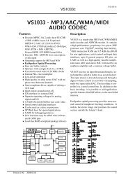
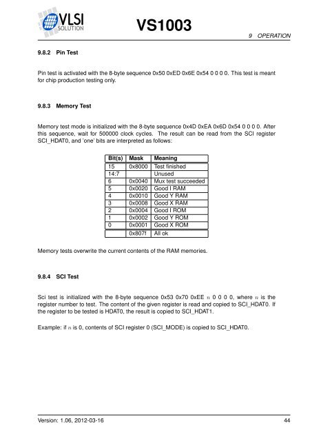
<strong>VS1003</strong>9 OPERATION9.8.2 Pin TestPin test is activated with the 8-byte sequence 0x50 0xED 0x6E 0x54 0 0 0 0. This test is meantfor chip production testing only.9.8.3 Memory TestMemory test mode is initialized with the 8-byte sequence 0x4D 0xEA 0x6D 0x54 0 0 0 0. Afterthis sequence, wait for 500000 clock cycles. The result can be read from the SCI registerSCI_HDAT0, and ’one’ bits are interpreted as follows:Bit(s) Mask Meaning15 0x8000 Test finished14:7 Unused6 0x0040 Mux test succeeded5 0x0020 Good I RAM4 0x0010 Good Y RAM3 0x0008 Good X RAM2 0x0004 Good I ROM1 0x0002 Good Y ROM0 0x0001 Good X ROM0x807fAll okMemory tests overwrite the current contents of the RAM memories.9.8.4 SCI TestSci test is initialized with the 8-byte sequence 0x53 0x70 0xEE n 0 0 0 0, where n is theregister number to test. The content of the given register is read and copied to SCI_HDAT0. Ifthe register to be tested is HDAT0, the result is copied to SCI_HDAT1.Example: if n is 0, contents of SCI register 0 (SCI_MODE) is copied to SCI_HDAT0.Version: 1.06, 2012-03-16 44