
You also want an ePaper? Increase the reach of your titles
YUMPU automatically turns print PDFs into web optimized ePapers that Google loves.
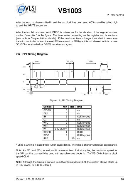
<strong>VS1003</strong>7 SPI BUSESAfter the word has been shifted in and the last clock has been sent, XCS should be pulled highto end the WRITE sequence.After the last bit has been sent, DREQ is driven low for the duration of the register update,marked “execution” in the figure. The time varies depending on the register and its contents(see table in Chapter 8.6 for details). If the maximum time is longer than what it takes fromthe microcontroller to feed the next SCI command or SDI byte, it is not allowed to finish a newSCI/SDI operation before DREQ has risen up again.7.6 SPI Timing DiagramtXCSStWLtWHtXCSHXCS0 1 14 15 1630 31tXCSSCKSISOtZtHtSUtVtDISFigure 12: SPI Timing Diagram.Symbol Min Max UnittXCSS 5 nstSU 0 nstH 2 CLKI cyclestZ 0 nstWL 2 CLKI cyclestWH 2 CLKI cyclestV 2 (+ 25ns 1 ) CLKI cyclestXCSH 1 CLKItXCS 2 CLKI cyclestDIS 10 ns1 25ns is when pin loaded with 100pF capacitance. The time is shorter with lower capacitance.Note: As tWL and tWH, as well as tH require at least 2 clock cycles, the maximum speed forthe SPI bus that can easily be used with asynchronous clocks is 1/7 of <strong>VS1003</strong>’s internal clockspeed CLKI.Note: Although the timing is derived from the internal clock CLKI, the system always starts upin 1.0× mode, thus CLKI=XTALI.Version: 1.06, 2012-03-16 20