You also want an ePaper? Increase the reach of your titles
YUMPU automatically turns print PDFs into web optimized ePapers that Google loves.
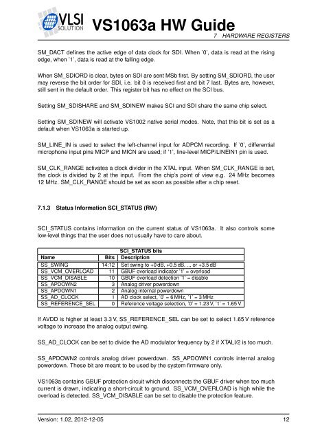
<strong>VS1063</strong>a HW <strong>Guide</strong>7 HARDWARE REGISTERSSM_DACT defines the active edge of data clock for SDI. When ’0’, data is read at the risingedge, when ’1’, data is read at the falling edge.When SM_SDIORD is clear, bytes on SDI are sent MSb first. By setting SM_SDIORD, the usermay reverse the bit order for SDI, i.e. bit 0 is received first and bit 7 last. Bytes are, however,still sent in the default order. This register bit has no effect on the SCI bus.Setting SM_SDISHARE and SM_SDINEW makes SCI and SDI share the same chip select.Setting SM_SDINEW will activate VS1002 native serial modes. Note, that this bit is set as adefault when <strong>VS1063</strong>a is started up.SM_LINE_IN is used to select the left-channel input for ADPCM recording. If ’0’, differentialmicrophone input pins MICP and MICN are used; if ’1’, line-level MICP/LINEIN1 pin is used.SM_CLK_RANGE activates a clock divider in the XTAL input. When SM_CLK_RANGE is set,the clock is divided by 2 at the input. From the chip’s point of view e.g. 24 MHz becomes12 MHz. SM_CLK_RANGE should be set as soon as possible after a chip reset.7.1.3 Status Information SCI_STATUS (RW)SCI_STATUS contains information on the current status of <strong>VS1063</strong>a. It also controls somelow-level things that the user does not usually have to care about.SCI_STATUS bitsName Bits DescriptionSS_SWING 14:12 Set swing to +0 dB, +0.5 dB, .., or +3.5 dBSS_VCM_OVERLOAD 11 GBUF overload indicator ’1’ = overloadSS_VCM_DISABLE 10 GBUF overload detection ’1’ = disableSS_APDOWN2 3 Analog driver powerdownSS_APDOWN1 2 Analog internal powerdownSS_AD_CLOCK 1 AD clock select, ’0’ = 6 MHz, ’1’ = 3 MHzSS_REFERENCE_SEL 0 Reference voltage selection, ’0’ = 1.23 V, ’1’ = 1.65 VIf AVDD is higher at least 3.3 V, SS_REFERENCE_SEL can be set to select 1.65 V referencevoltage to increase the analog output swing.SS_AD_CLOCK can be set to divide the AD modulator frequency by 2 if XTALI/2 is too much.SS_APDOWN2 controls analog driver powerdown. SS_APDOWN1 controls internal analogpowerdown. These bit are meant to be used by the system firmware only.<strong>VS1063</strong>a contains GBUF protection circuit which disconnects the GBUF driver when too muchcurrent is drawn, indicating a short-circuit to ground. SS_VCM_OVERLOAD is high while theoverload is detected. SS_VCM_DISABLE can be set to disable the protection feature.Version: 1.02, 2012-12-05 12


