Heterostructure Band Engineering of Type-II InAs/GaSb Superlattice ...
Heterostructure Band Engineering of Type-II InAs/GaSb Superlattice ...
Heterostructure Band Engineering of Type-II InAs/GaSb Superlattice ...

Create successful ePaper yourself
Turn your PDF publications into a flip-book with our unique Google optimized e-Paper software.
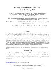
Spectral Response (a.u.)<br />
1.4<br />
1.2<br />
1.0<br />
0.8<br />
0.6<br />
0.4<br />
0.2<br />
λc=10.8 μm<br />
PbIbN<br />
PIN<br />
λc=11.0 μm<br />
0.0<br />
8.5 9.0 9.5 10.0 10.5 11.0 11.5 12.0 12.5<br />
Wavelength (μm)<br />
Figure 3. Spectral response <strong>of</strong> PIN and PbIbN devices at 77K with cut<strong>of</strong>f wavelength <strong>of</strong> 11.0 µm and 10.8 µm<br />
respectively.<br />
Current-voltage (IV) characteristics were measured for all the devices from 30K to 250K using HP4145 semiconductor<br />
parameter analyzer. Figure 4(a) shows temperature dependent dark current characteristics for PbIbN detector and figure<br />
4(b) compares it with PIN detector at 77K. At lower temperatures, these devices show asymmetric diode characteristic<br />
while at higher temperatures the I-V curves become symmetric owing to the dark current due to thermal generation <strong>of</strong><br />
carriers.<br />
J (A/cm 2 )<br />
100<br />
10<br />
1<br />
0.1<br />
0.01<br />
1E-3<br />
1E-4<br />
1E-5<br />
-3 -2 -1 0 1 2 3<br />
Bias (V)<br />
(a)<br />
77K<br />
150K<br />
200K<br />
250K<br />
J (A/cm 2 )<br />
100<br />
10<br />
1<br />
0.1<br />
0.01<br />
1E-3<br />
1E-4<br />
1E-5<br />
1E-6<br />
77K<br />
-1.5 -1.0 -0.5 0.0 0.5 1.0 1.5<br />
Bias (V)<br />
(b)<br />
PIN<br />
PbIbN<br />
Figure 4. (a) Variable temperature dark current characteristics <strong>of</strong> PbIbN detector, (b) dark current density comparison<br />
<strong>of</strong> PbIbN design with PIN design at 77K.<br />
As shown in figure 4(b), PbIbN design shows significantly improved performance over PIN detector. The major sources<br />
<strong>of</strong> dark current in a PIN detector are thermal generation <strong>of</strong> carriers, SRH current, tunneling currents and minority carrier<br />
diffusion current. In PbIbN design, an electron barrier <strong>of</strong> wider bandgap material is placed between P contact layer and<br />
absorber region I. When the detector is operated under reverse bias, photogenerated holes move towards P contact while<br />
electrons move towards N contact. The eB layer allows unimpeded flow <strong>of</strong> holes while blocking electrons and also leads<br />
Proc. <strong>of</strong> SPIE Vol. 7660 76601T-4<br />
Downloaded from SPIE Digital Library on 21 May 2010 to 64.106.37.191. Terms <strong>of</strong> Use: http://spiedl.org/terms