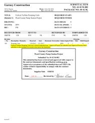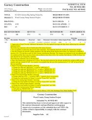
26 29 23-001A Med Voltage VFD Resubmittal - Garney Construction
26 29 23-001A Med Voltage VFD Resubmittal - Garney Construction
26 29 23-001A Med Voltage VFD Resubmittal - Garney Construction

Create successful ePaper yourself
Turn your PDF publications into a flip-book with our unique Google optimized e-Paper software.
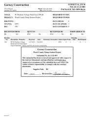
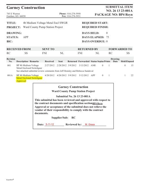
<strong>Garney</strong> <strong>Construction</strong><br />
785 E Warren<br />
Gardner, KS 66030<br />
Phone: 816-278-5950<br />
Fax: 816-278-5931<br />
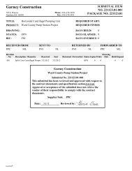
SUBMITTAL ITEM<br />
O. <strong>26</strong> 13 <strong>23</strong>-<strong>001A</strong><br />
PACKAGE O: BP4 Reyn<br />
TITLE:<br />
PROJECT:<br />
DRAWIG:<br />
STATUS:<br />
BIC:<br />
4b <strong>Med</strong>ium <strong>Voltage</strong> Metal Encl SWGR<br />
Ward County Pump Station Project<br />
APP<br />
REQUIRED START:<br />
REQUIRED FIISH:<br />
DAYS HELD: 0<br />
DAYS ELAPSED: 75<br />
DAYS OVERDUE: 0<br />
RECEIVED FROM<br />
RC<br />
SS<br />
SET TO<br />
FNI<br />
NL<br />
RETURED BY<br />
FNI NL<br />
FORWARDED TO<br />
RC<br />
SS<br />
Revision<br />
o.<br />
Description / Remarks<br />
Received<br />
Sent<br />
Drawing<br />
Returned Forwarded Status Sepias Prints Date HeldElapsed<br />
001 BP 4b <strong>Med</strong>ium <strong>Voltage</strong><br />
Metal Enclosed Switchgear<br />
2/27/2012 2/28/2012 3/9/2012 3/13/2012 ANR 0 1 0 15<br />
See attached submittal review comments from Jeff Hensley and Rebecca Sandoval<br />
<strong>001A</strong><br />
BP 4b <strong>Med</strong>ium <strong>Voltage</strong><br />
Metal Enclosed Switchgear<br />
Approved<br />
4/20/2012 4/20/2012 5/9/2012 5/12/2012 APP 0 1 1 22<br />
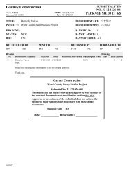
<strong>Garney</strong> <strong>Construction</strong><br />
Ward County Pump Station Project<br />
Submittal o. <strong>26</strong> 13 <strong>23</strong>-<strong>001A</strong><br />
This submittal has been reviewed and approved with respect to<br />
the contract documents and specification sectionBP4 Reyn<br />
Approval or acceptance of the submittal does not relieve the<br />
vendor of their responsibility to comply with the contract<br />
documents.<br />
Supplier/Sub: RC<br />
Date: ______________ 5-11-12 Reviewed by: _________________<br />
M. Grace<br />
Expedition ®
SUBMITTALS<br />
https://projectdox.freese.com/imarkupwg/form.aspformid=6415&wfdirect=&debug=&co...<br />
Page 1 of 2<br />
5/11/2012<br />
Project No:<br />
Project:<br />
Client:<br />
Contractor:<br />
CMD11<strong>26</strong>9D<br />
CMAR Ward County Transmission System - Electrical<br />
Equipment<br />
Colorado River Municipal Water District<br />
<strong>Garney</strong><br />
Shop Drawing #<strong>001A</strong><br />
<strong>Resubmittal</strong> - <strong>Med</strong>ium <strong>Voltage</strong> Metal Enclosed Switchgear<br />
WORKFLOW COMPLETED 5/9/2012 7:38 AM<br />
SUBMITTAL INFORMATION<br />
SUBMITTAL<br />
TYPE:<br />
SUBMITTAL #: CONTRACTOR REF #: SPEC SECTION: PLAN SHEET: SUBMITTAL STATUS:<br />
Shop<br />
Drawing<br />
<strong>001A</strong><br />
SD-10 Approved<br />
SUBMITTAL<br />
DESCRIPTION:<br />
<strong>Resubmittal</strong> - <strong>Med</strong>ium <strong>Voltage</strong> Metal Enclosed Switchgear<br />
UPLOAD SUPPORTING DOCUMENTS<br />
SD-<strong>001A</strong> <strong>Resubmittal</strong> - <strong>Med</strong>ium <strong>Voltage</strong> Metal Enclosed Switchgear.pdf<br />
4/<strong>23</strong>/2012 8:25 AM Jane Jenks<br />
CONTRACTOR CERTIFICATION<br />
CONTRACTOR COMMENTS:<br />
Submitted via e-mail<br />
HOW WILL THE COPIES BE SUBMITTED:<br />
Electronic<br />
NUMBER OF COPIES SUBMITTED: 1<br />
This shop drawing has been reviewed by the Contractor and certified to be in strict conformance with the Contract Documents as modified by addenda, field orders, and<br />
change orders. Deviations can only be approved by field order or change order. Approval is only for conformance with the design concept of the project and compliance<br />
with the intent of the information given in the Contract Documents. Contractor is responsible for dimensions to be confirmed and correlated at the job site; for information<br />
that pertains solely to the fabrication processes or to techniques of construction; and for the work of all trades.<br />
SUBMITTED BY: Jane Jenks<br />
DATE: 4/<strong>23</strong>/2012 8:25 AM<br />
REVIEWER COMMENTS<br />
REVIEWER NAME: REVIEWER EMAIL: COMPANY / ORGANIZATION DATE SENT: DATE<br />
COMPLETED:<br />
Jeff Hensley<br />
jnh@freese.com<br />
4055 International Plaza<br />
4/<strong>23</strong>/2012 5/7/2012<br />
REVIEWER<br />
COMMENTS:<br />
Approved.<br />
REVIEWER NAME: REVIEWER EMAIL: COMPANY / ORGANIZATION DATE SENT: DATE<br />
COMPLETED:<br />
Rebecca<br />
Sandoval<br />
rs@freese.com<br />
Freese and Nichols, Inc<br />
4/<strong>23</strong>/2012<br />
5/2/2012<br />
REVIEWER<br />
COMMENTS:<br />
5/2/12<br />
Refer to Jeff Hensley for additional comments.<br />
Approved.<br />
UPLOAD SUPPORTING REVIEW DOCUMENTS<br />
DISPLAY ROUTING SLIP
SUBMITTALS<br />
https://projectdox.freese.com/imarkupwg/form.aspformid=6415&wfdirect=&debug=&co...<br />
Page 2 of 2<br />
5/11/2012<br />
Current Workflow Step: DCS Admin: Jane Jenks Workflow Initiator: Jane Jenks<br />
(Click on the Names above to Email User)<br />
FNI Forms v1.04
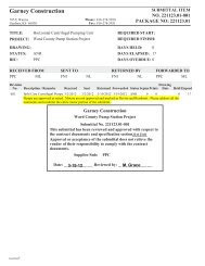
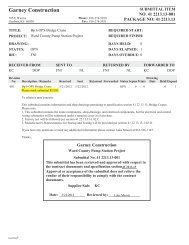
<strong>Garney</strong> <strong>Construction</strong><br />
785 E Warren<br />
Gardner, KS 66030<br />
Phone: 816-278-5950<br />
Fax: 816-278-5931<br />
SUBMITTAL ITEM<br />
O. <strong>26</strong> <strong>29</strong> <strong>23</strong>.1-<strong>001A</strong><br />
PACKAGE O: BP4 Reyn<br />
TITLE:<br />
PROJECT:<br />
DRAWIG:<br />
STATUS:<br />
BIC:<br />
4e <strong>Med</strong>ium <strong>Voltage</strong> <strong>VFD</strong>'s<br />
Ward County Pump Station Project<br />
OPN<br />
FNI<br />
REQUIRED START:<br />
REQUIRED FIISH:<br />
DAYS HELD: 0<br />
DAYS ELAPSED: 53<br />
DAYS OVERDUE: 0<br />
RECEIVED FROM<br />
RC<br />
SS<br />
SET TO<br />
FNI<br />
NL<br />
RETURED BY<br />
FNI NL<br />
FORWARDED TO<br />
RC<br />
SS<br />
Revision<br />
o.<br />
Description / Remarks<br />
Received<br />
Sent<br />
Drawing<br />
Returned Forwarded Status Sepias Prints Date HeldElapsed<br />
001 Bid Pkg 4e <strong>Med</strong>ium <strong>Voltage</strong><br />
<strong>VFD</strong>'s<br />
2/27/2012 2/28/2012 3/9/2012 3/13/2012 ANR 0 1 0 15<br />
Please address engineer's comments and resubmit entire package. Please release for fabrication and delivery per engineer's<br />
comments<br />
002 Bid Pkg 4e <strong>Med</strong>ium <strong>Voltage</strong><br />
<strong>VFD</strong>'s<br />
4/20/2012 4/20/2012 OPN 0 0 0 0<br />
Urgent <strong>Resubmittal</strong> - <strong>Garney</strong> and FNI will review concurrently.<br />
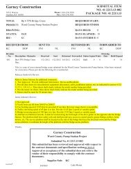
<strong>Garney</strong> <strong>Construction</strong><br />
Ward County Pump Station Project<br />
Submittal o. <strong>26</strong> <strong>29</strong> <strong>23</strong>.1-<strong>001A</strong><br />
This submittal has been reviewed and approved with respect to<br />
the contract documents and specification sectionBP4 Reyn<br />
Approval or acceptance of the submittal does not relieve the<br />
vendor of their responsibility to comply with the contract<br />
documents.<br />
Supplier/Sub: RC<br />
Date: ______________ Reviewed by: _________________<br />
Expedition ®
SUBMITTALS<br />
https://projectdox.freese.com/imarkupwg/form.aspformid=6415&wfdirect=&debug=&co...<br />
Page 1 of 2<br />
3/13/2012<br />
Project No:<br />
Project:<br />
Client:<br />
Contractor:<br />
CMD11<strong>26</strong>9D<br />
CMAR Ward County Transmission System - Electrical<br />
Equipment<br />
Colorado River Municipal Water District<br />
<strong>Garney</strong><br />
Shop Drawing #004<br />
URGENT Bid Package 4e <strong>Med</strong>ium <strong>Voltage</strong> <strong>VFD</strong>'s<br />
WORKFLOW COMPLETED 3/9/2012 11:<strong>29</strong> AM<br />
SUBMITTAL INFORMATION<br />
SUBMITTAL<br />
TYPE:<br />
Shop<br />
Drawing<br />
SUBMITTAL<br />
DESCRIPTION:<br />
SUBMITTAL #: CONTRACTOR REF #: SPEC SECTION: PLAN SHEET: SUBMITTAL STATUS:<br />
004<br />
<strong>26</strong> <strong>29</strong> <strong>23</strong>.01-001<br />
URGENT Bid Package 4e <strong>Med</strong>ium <strong>Voltage</strong> <strong>VFD</strong>'s<br />
<strong>26</strong> <strong>29</strong> <strong>23</strong>.01<br />
Approved As Noted, Revise<br />
and Resubmit, Additional<br />
Information Required<br />
UPLOAD SUPPORTING DOCUMENTS<br />
<strong>26</strong> <strong>29</strong> <strong>23</strong>.01 - 001.pdf 2/28/2012 7:52 PM Marcus Grace<br />
CONTRACTOR CERTIFICATION<br />
CONTRACTOR COMMENTS:<br />
Urgent Submittal - <strong>Garney</strong> and FNI will review concurrently<br />
HOW WILL THE COPIES BE SUBMITTED:<br />
Electronic<br />
NUMBER OF COPIES SUBMITTED: 1<br />
This shop drawing has been reviewed by the Contractor and certified to be in strict conformance with the Contract Documents as modified by addenda, field orders, and<br />
change orders. Deviations can only be approved by field order or change order. Approval is only for conformance with the design concept of the project and compliance<br />
with the intent of the information given in the Contract Documents. Contractor is responsible for dimensions to be confirmed and correlated at the job site; for information<br />
that pertains solely to the fabrication processes or to techniques of construction; and for the work of all trades.<br />
SUBMITTED BY: Marcus Grace<br />
DATE: 2/28/2012 7:53 PM<br />
REVIEWER COMMENTS<br />
REVIEWER NAME: REVIEWER EMAIL: COMPANY / ORGANIZATION DATE<br />
SENT:<br />
Jeff Hensley<br />
jnh@freese.com<br />
4055 International Plaza<br />
3/1/2012<br />
DATE<br />
COMPLETED:<br />
3/8/2012<br />
REVIEWER<br />
COMMENTS:
SUBMITTALS<br />
https://projectdox.freese.com/imarkupwg/form.aspformid=6415&wfdirect=&debug=&co...<br />
Page 2 of 2<br />
3/13/2012<br />
1. Approved as Noted. Additional information required. Formally respond to all comment in<br />
writing and provide revised data per review comments.<br />
2. The harmonic analysis shall be done in accordance with Specification <strong>26</strong> <strong>29</strong> <strong>23</strong>.01, paragraph<br />
1.07. The different scenarios required per paragraph 1.07.C. need to be provided at the different<br />
speeds. Provide paragraph clearly listing Utility data used to perform the study. The write-up in<br />
the report shall clearly identify the PCC and give an explanation of the results for each<br />
operating scenario.<br />
3. The harmonic analysis shall clearly identify the PCC at the TPS site as being the 4160V main<br />
switchgear. It currently shows the PCC at the 12.47kV bus.<br />
4. Update harmonic analysis based on comments listed above.<br />
5. Verify <strong>VFD</strong> meets the requirements for true power factor and efficiency as required per the<br />
<strong>VFD</strong> specification.<br />
6. Rearrange the following pushbutton and indicating lights so that they are physically located<br />
horizontally next to each other: Start/Stop, Pump Run/Pump Stop, Valve Open/Closed. Update<br />
drawing to reflect this.<br />
7. One the one-line diagram, a separate external 120V circuit shall be shown going to the motor<br />
space heater. This external 120V circuit shall be shown going through the normally closed SHR<br />
contact. Update all drawings and terminal block layout drawings to reflect this.<br />
8. On one-line diagram add note that 120V for CSH is for temporary storage only.<br />
9. For the three line diagram showing the Multilin 469, the voltage inputs shall be wired to the<br />
Multilin. Update drawing to reflect this.<br />
10. Per <strong>VFD</strong> specification show how the conduits for the control and instrumentation will<br />
physically be terminated to the top of the <strong>VFD</strong>. Show how the cables can be routed in the<br />
spaces provided.<br />
11. Show fuse sizes, CT ratios and HPs on all applicable drawings.<br />
12. In the control schematic for the <strong>VFD</strong>, a <strong>VFD</strong> fault contact shall be wired in series with the<br />
MPR Trip to open the circuit and de-energize CR1. Update drawings to reflect this.<br />
13. The normally open contact CTR2 in the control schematic terminated to terminal 403D<br />
should be a normally closed contact that opens when the timer has timed out.<br />
14. The SCADA Reset normally open contact in the control schematic shall be a normally<br />
closed contact that opens to reset the circuit.<br />
15. Wiring the 4-20mA signals and RTD directly the Card and 469 relay are acceptable.<br />
REVIEWER NAME: REVIEWER EMAIL: COMPANY / ORGANIZATION DATE<br />
SENT:<br />
Rebecca<br />
Sandoval<br />
rs@freese.com<br />
Freese and Nichols, Inc<br />
3/1/2012<br />
DATE<br />
COMPLETED:<br />
3/8/2012<br />
REVIEWER<br />
COMMENTS:<br />
3/8/12<br />
Approved as Noted. Provide Additional Information. Revise and Resubmit. Provide a written<br />
response to each comment on a separate sheet of paper.<br />
See attached for complete comments by R.Sandoval.<br />
Refer to Jeff Hensley for additional comments.<br />
UPLOAD SUPPORTING REVIEW DOCUMENTS<br />
CMD SD-04 MV <strong>VFD</strong> Comments RSandoval 03.08.12.pdf<br />
Remove 3/8/2012 5:07 PM Rebecca Sandoval<br />
DISPLAY ROUTING SLIP<br />
Current Workflow Step: DCS Admin: Debby Greer Workflow Initiator: Marcus Grace<br />
(Click on the Names above to Email User)<br />
FNI Forms v1.04
Rebecca Sandoval Freese and Nichols, Inc.<br />
CMD11<strong>26</strong>9- Contact C4 – Electrical Equipment SD-004 – <strong>Med</strong>ium <strong>Voltage</strong> <strong>VFD</strong>s<br />
3/08/2012<br />
1. Approved as Noted. Provide Additional Information. Revise and Resubmit. Provide a written response to each comment on a<br />
separate sheet of paper.<br />
2. Show the total height of the equipment on the drawings.<br />
3. The <strong>VFD</strong> shall be top entry and exit. Currently this is indicated on the drawings as such but the Load/Controller Data sheet<br />
indicates bottom entry.<br />
4. As indicated in section <strong>26</strong> <strong>29</strong> <strong>23</strong>.01-12, 2.04.D.2 the lights, push buttons, switches, displays, etc. shall be mounted no higher<br />
than 5’-6” AFF which shall include the height of the 4” housekeeping pad. Currently the submittal indicates that these devices<br />
will be located 6’-2” AFF (including the 4” housekeeping pad). If the devices cannot be moved lower then locate the nameplate<br />
for these devices so that it is shown below the device rather than above it.<br />
6. Refer to electrical drawing sheet 16: a) Show the valve switch position table indicated on the FNI TPS <strong>VFD</strong> Pump Control<br />
Schematic. b) See attached mark-ups for additional comments to the control schematic. Changes include removing one of the<br />
duplicate pressure switches that was shown on the FNI schematic. Update all associated drawings to reflect this.<br />
1. Refer to electrical drawing sheet 7, terminals 636 & 636A: The Hand/Off/SCADA label needs to indicate the designation “OOX”<br />
and not “OXO”.<br />
2. Refer to electrical drawing sheet 9: There isn’t any pump bearing RTDs at this site.<br />
3. Drawings shall show cable sizes for the incoming and outgoing sections that the <strong>VFD</strong> can accept as indicated in section <strong>26</strong> <strong>29</strong><br />
<strong>23</strong>.01-4, 1.04.A.2.d.7).<br />
4. Refer to electrical drawing sheet 10: In the bottom left corner there are two lines of text on top of each other.<br />
5. Nameplates shall be black with white letters as indicated in section <strong>26</strong> 13 <strong>23</strong>-12, 2.02.H. Currently the submitted indicates the<br />
nameplates will be white with black letters. Update all associated drawings to reflect this.<br />
Jeff Hensley Comments<br />
1. Approved as Noted. Additional information required. Formally respond to all comment in writing and provide revised data per review<br />
comments.<br />
2. The harmonic analysis shall be done in accordance with Specification <strong>26</strong> <strong>29</strong> <strong>23</strong>.01, paragraph 1.07. The different scenarios required per<br />
paragraph 1.07.C. need to be provided at the different speeds. Provide paragraph clearly listing Utility data used to perform the study. The<br />
write-up in the report shall clearly identify the PCC and give an explanation of the results for each operating scenario.<br />
3. The harmonic analysis shall clearly identify the PCC at the TPS site as being the 4160V main switchgear. It currently shows the PCC at the<br />
12.47kV bus.<br />
4. Update harmonic analysis based on comments listed above.<br />
5. Verify <strong>VFD</strong> meets the requirements for true power factor and efficiency as required per the <strong>VFD</strong> specification.<br />
6. Rearrange the following pushbutton and indicating lights so that they are physically located horizontally next to each other: Start/Stop, Pump<br />
Run/Pump Stop, Valve Open/Closed. Update drawing to reflect this.<br />
7. One the one-line diagram, a separate external 120V circuit shall be shown going to the motor space heater. This external 120V circuit shall be<br />
shown going through the normally closed SHR contact. Update all drawings and terminal block layout drawings to reflect this.<br />
8. On one-line diagram add note that 120V for CSH is for temporary storage only.<br />
9. For the three line diagram showing the Multilin 469, the voltage inputs shall be wired to the Multilin. Update drawing to reflect this.<br />
10. Per <strong>VFD</strong> specification show how the conduits for the control and instrumentation will physically be terminated to the top of the <strong>VFD</strong>. Show how<br />
the cables can be routed in the spaces provided.<br />
11. Show fuse sizes, CT ratios and HPs on all applicable drawings.<br />
12. In the control schematic for the <strong>VFD</strong>, a <strong>VFD</strong> fault contact shall be wired in series with the MPR Trip to open the circuit and de-energize CR1.<br />
Update drawings to reflect this.<br />
13. The normally open contact CTR2 in the control schematic terminated to terminal 403D should be a normally closed contact that opens when the<br />
timer has timed out.<br />
14. The SCADA Reset normally open contact in the control schematic shall be a normally closed contact that opens to reset the circuit.<br />
15. Wiring the 4-20mA signals and RTD directly the Card and 469 relay are acceptable.
135 Dundas Street<br />
Cambridge ON N1R5X1<br />
CANADA<br />
Tel. +1.519.740.4100<br />
Fax +1.519.740.9871<br />
The Reynolds Company<br />
Project Name: Ward County Water Supply<br />
Rockwell Automation Order Number: 7012577<br />
Subject: Response to <strong>VFD</strong> submittal review comments<br />
Date: March 28, 2012<br />
Rebecca Sandoval Comments / RA response<br />
- See current document.<br />
- The total height is shown on individual structural detail pages. See 7012577-001-12D<br />
pg. 2 and on.<br />
- 7012577-001-12D pg. 12, Unit 2A: The "Bottom" load cable exit direction refers to an<br />
internal inter-cabling connection. The drawing has been revised to state as such.<br />
- Height of the pilot devices does not exceed the specified height limit. See revised<br />
7012577-001-12DL.<br />
- Drawing revised. The valve limit switch position table is shown on pg. 2, referenced in<br />
pg. 16.<br />
- Drawing revised.<br />
- Drawing revised.
- See 7012577-001-12D pg. 5 (line cable), and pg. 12 (load cable).<br />
- Drawing revised.<br />
- Drawing revised.<br />
-<br />
Jeff Hensley Comments / RA response<br />
- See current document.<br />
- See Tab 6 revised harmonic analysis. The revised analysis includes three additional<br />
scenarios, one, two and three <strong>VFD</strong>’s running all at 100% speed.<br />
- See Tab 6 revised harmonic analysis<br />
- See Tab 6 revised harmonic analysis<br />
- See Tab 0 - Ward County - Expected <strong>VFD</strong> Efficiency.<br />
- See revised door layout in Tab 1 - 7012577-001-12DL.<br />
- The drawing has been revised to show a separate 120V external supply. However, it is<br />
our standard to omit the SHR contact on the one-line diagram.<br />
- Drawing revised.<br />
- Drawing revised.<br />
- See revised top plate on 7012577-001-12D pg. 4. The new arrangement can<br />
accommodate 8x 2" conduits in total for control cables.<br />
- Drawing revised.
- Drawing revised.<br />
- Drawing revised.<br />
- Drawing revised.<br />
- Acknowledged.<br />
Regards,<br />
Ken Hilderley<br />
Rockwell Automation<br />
Project Manager – MV Drives<br />
Ph: 519 740 4736<br />
Email: khilderley@ra.rockwell.com
Rockwell Automation Transmittal – Approval Drawings/Documentation<br />
Date: March 28, 2012<br />
To:<br />
Attention:<br />
Rockwell Automation<br />
<strong>23</strong>04 Tarpley Road<br />
Carrollton, Texas, USA<br />
75006<br />
972 417 5400<br />
Kevin Nowak<br />
Subject/Project:<br />
Customer:<br />
TRANSMISSION PUMP STATION<br />
WARD COUNTY WATER SUPPLY<br />
Distributor:<br />
THE REYNOLDS COMPANY<br />
Distributor PO#: 1638098-00<br />
RA Order#: 7012577 Item(s): 001 to 020<br />
The conformed submittal has been submitted for information only. The information drawing(s) /<br />
documentation are only submitted when engineering is finalized, at which time manufacturing will<br />
commence. If changes are submitted, the order will then be subject to revision charges and<br />
possible delays in shipment.<br />
1 of 1
RA Order #: 7012577<br />
Submittal Documentation<br />
<strong>Med</strong>ium <strong>Voltage</strong> Equipment<br />
PowerFlex 7000 <strong>Med</strong>ium <strong>Voltage</strong> Drive<br />
Ward County Water Supply<br />
Transmission Pump Station<br />
Description<br />
Table of Contents Page 1 of 3<br />
Rockwell Publication<br />
Transmittal – Ward County<br />
Table of Contents (this document)<br />
Comments and Clarifications for Section <strong>26</strong> <strong>29</strong> <strong>23</strong>.01<br />
<strong>VFD</strong>-Motor Compatibility Letter<br />
Ward County – Expected <strong>VFD</strong> Efficiency<br />
Warranty Letter<br />
Tab 1 Dimensional Drawings<br />
Dimensional Drawing – <strong>VFD</strong>-TPSP1<br />
Dimensional Drawing – <strong>VFD</strong>-TPSP2<br />
Dimensional Drawing – <strong>VFD</strong>-TPSP3<br />
Dimensional Drawing – <strong>VFD</strong>-TPSP4<br />
Plan Layout Drawing<br />
Elevation Drawing<br />
Line Cable Connection Drawing<br />
Tab 2 Electrical Drawings<br />
Electrical Drawing<br />
Tab 3 BOM and Spare Parts<br />
Preliminary Bill of Materials – <strong>VFD</strong> Output Contactor<br />
Preliminary Bill of Materials – <strong>VFD</strong> Input Contactor / FPT<br />
Preliminary Bill of Materials – Variable Frequency Drive<br />
Spare Parts List – Furnished<br />
7012577-001-12D_2<br />
7012577-002-12D_2<br />
7012577-003-12D_2<br />
7012577-004-12D_2<br />
7012577-001-12PL<br />
7012577-001-12DL<br />
7012577-001-12E_2<br />
7012577-017-FBOM<br />
7012577-001-FBOM<br />
7012577-002-FBOM<br />
Publication: 7012577 – March 2012
RA Order #: 7012577<br />
Submittal Documentation<br />
<strong>Med</strong>ium <strong>Voltage</strong> Equipment<br />
PowerFlex 7000 <strong>Med</strong>ium <strong>Voltage</strong> Drive<br />
Ward County Water Supply<br />
Transmission Pump Station<br />
Description<br />
Table of Contents Page 2 of 3<br />
Rockwell Publication<br />
Tab 4 Component Datasheets<br />
469 Motor Protection System 80025-911<br />
Motor Protection Circuit Breakers<br />
140M<br />
IEC Non-Fused Disconnects<br />
194R<br />
Monitoring Safety Relays<br />
440R-G<strong>23</strong>215<br />
Eutatic Alloy Overload Relays 592<br />
DIN Rail Timing Relay<br />
700FS<br />
Heavy-Duty Industrial Relays<br />
700P<br />
30.5mm Push Buttons<br />
800H<br />
Fuse Holders<br />
1492FB<br />
Screw Connection Terminal Blocks<br />
1492J<br />
Supplementary Protector<br />
1492SP<br />
Current Transformer, Donut Type 80022-162<br />
Elapsed Time Meter 80025-413<br />
Curves, MV Fuses<br />
Curves, Potential Transformer Fuses<br />
Curves, TRM Fuses<br />
Curves, Overload Relay<br />
Zero Sequence Current Transformer, 50-0.025 80022-030<br />
Common Mode Choke, Heavy Duty 80022-146<br />
Control Power Transformer, 1kVA 80022-154<br />
Potential Transformer, 600VA 80022-164<br />
Control Power Transformer, 3kVA 80022-197<br />
AC Line Reactor 80022-210<br />
Input Sensing CT, 1000-1 80025-551<br />
Test Switch 80025-597<br />
Capacitor, Motor-Line Filter 800<strong>26</strong>-041<br />
Power Supply, IGDPS 800<strong>26</strong>-044<br />
Hall Effect Current Sensor, 4000-1 800<strong>26</strong>-387<br />
Icar Capacitor 800<strong>26</strong>-511<br />
Publication: 7012577 – March 2012
RA Order #: 7012577<br />
Submittal Documentation<br />
<strong>Med</strong>ium <strong>Voltage</strong> Equipment<br />
PowerFlex 7000 <strong>Med</strong>ium <strong>Voltage</strong> Drive<br />
Ward County Water Supply<br />
Transmission Pump Station<br />
Description<br />
Table of Contents Page 3 of 3<br />
Rockwell Publication<br />
Tab 4 Component Datasheets (continued)<br />
Power Supply, DC-to-DC 800<strong>26</strong>-518<br />
Power Supply, AC-DC (Pioneer 1500W) 800<strong>26</strong>-524<br />
Main Cooling Fan 800<strong>26</strong>-845<br />
400A Moulded Isolator Switch, Bolt-On 80154-544<br />
Vacuum Contactor 80158-691<br />
SGCT, 800A 80173-109<br />
Transient Surge Network 81000-748<br />
Printed Circuit Boards<br />
Tab 5 <strong>VFD</strong> Technical Data<br />
Ward County - Load Capability Curve<br />
PF7000B Heat Loss Information<br />
<strong>VFD</strong>-Motor Protection Parameters<br />
PowerFlex 7000 MV AC Drive Technical Data<br />
GK5.065<br />
7000-TD002B-EN-P<br />
Tab 6 Harmonic Analysis<br />
Ward County – Harmonic Report R2<br />
Tab 7 Factory Testing<br />
General Overview of Rockwell Automation Standard Testing<br />
Typical Test Procedures for MV Products<br />
<strong>Med</strong>ium and Low <strong>Voltage</strong> Test Procedures for PF7000<br />
7000 Family Quality Control Test Listing<br />
Q.C. Inspection Card – PowerFlex 7000<br />
ISO 9001 Certificate<br />
1500-TD220D-EN-E<br />
CSP-2490-198-03<br />
Publication: 7012577 – March 2012
135 Dundas Street<br />
Cambridge Ontario<br />
Canada N1R 5X1<br />
Tel. +1.519.581.7424<br />
Fax. +1.519.740.9871<br />
Ward County Water Supply – Transmission Pump Station<br />
Rockwell Automation Order Number: 7012577<br />
Subject: Comments and Clarifications for Spec Section <strong>26</strong> <strong>29</strong> <strong>23</strong>.01 up to and including Addendum 3<br />
Date: February 19, 2012<br />
__________________________________________________________________________________________________<br />
1.00 GENERAL<br />
1.01 WORK INCLUDED<br />
1.01.A-C Comply.<br />
1.02 QUALITY ASSURANCE<br />
1.02.A-F Comply.<br />
1.02.G As per Meeting Minutes dated January 25, 2012, Rockwell is awaiting FNI to provide the checklist on the<br />
required pump control tests.<br />
1.02.H Comply.<br />
1.03 STANDARDS<br />
1.03.A-G Acknowledged.<br />
1.04 SUBMITTALS<br />
1.04.A.1 Comply.<br />
1.04.A.2.a See current document.<br />
1.04.A.2.b See Tab 1.<br />
1.04.A.2.c See Tab 1.<br />
1.04.A.2.d.1-9 See Tab 1.<br />
1.04.A.2.d.10-13 See Tab 2.<br />
1.04.A.2.e See Tab 3.<br />
1.04.A.2.f-h See Tab 4.<br />
1.04.A.2.i See Tab 3.<br />
1.04.A.2.j-k See Tab 0.<br />
1.04.A.2.l-m See Tab 5.<br />
1.04.A.2.n Not applicable.<br />
1.04.A.2.o See Tab 5.<br />
1.04.A.2.p See Tab 6.<br />
1.04.A.2.q Comply: Field test procedures to be submitted for approval two weeks prior to testing as specified.<br />
1.04.A.2.r Comply.<br />
1.04.A.3-4 Comply.<br />
1.04.A.5 NETA ATS is not within RA's scope of supply.<br />
1.04.A.6-8 Comply.<br />
1.05 DELIVERY, STORAGE AND HANDLING<br />
1.05.A-D Comply.<br />
1.05.E RA standard 150W (120V) cabinet space heaters shall be provided.<br />
Page 1 of 3
1.06 WARRANTY<br />
1.06.A-C Comply.<br />
1.07 HARMONIC ANALYSIS<br />
1.07.A-I Comply.<br />
2.00 PRODUCTS<br />
2.01 GENERAL<br />
2.01.A Comply.<br />
2.01.B The Drive Input Contactor unit consists of a fused non-load-break isolation switch as per 2.02.B.<br />
2.01.C-D Comply.<br />
2.02 ALLEN-BRADLEY <strong>VFD</strong>'S<br />
2.02.A-C Comply.<br />
2.03 Not Applicable<br />
2.04 VARIABLE FREQUENCY DRIVES<br />
2.04.A-C.2 Comply.<br />
2.04.C.3 The <strong>VFD</strong> cooling fans are controlled by internal pressure sensor instead of a thermostat.<br />
2.04.C.4-8 Comply.<br />
2.04.D.1 Comply.<br />
2.04.D.2 Exception: See Elevation Drawing in Tab 1.<br />
2.04.D.3 Comply.<br />
2.04.E.1 The <strong>VFD</strong> lineup has total length of 207.54", which includes the input/output contactors and the fan power<br />
transformer cabinet. See Tab 1 – 7012577-001-12D.<br />
2.04.E.2 The RA standard CT's at 300:5 have a class C20 accuracy. C200 refers to CT's with much higher primary<br />
current ratings, which is not applicable in this project.<br />
2.04.E.3-5 Comply.<br />
2.04.E.6 RA standard Crompton Elapsed Time Meter shall be provided. See 80025-413 in Tab 4.<br />
2.04.E.7-10 Comply.<br />
2.04.E.11 RA standard 1492-J4 terminal blocks shall be provided. See 1494J in Tab 4.<br />
2.04.E.12 Comply.<br />
2.04.E.13 The <strong>VFD</strong> cooling fans are controlled by internal pressure sensor instead of a thermostat.<br />
2.04.E.14-17 Comply.<br />
2.04.F Comply.<br />
2.04.G.1.a-h Comply.<br />
2.04.G.1.i 3 CT’s and 1 GFCT of RA standard shall be provided.<br />
2.04.G.1.j Comply.<br />
2.04.G.1.k Digital I/O's will be wired to terminal blocks. It is advised that the analog signals be wired directly onto<br />
the respective device terminals (i.e. speed reference, speed feedback, and RTD's).<br />
2.04.H-J Comply.<br />
3.00 EXECUTION<br />
3.01 GENERAL<br />
3.01.A-B Comply.<br />
3.02 INSTALLATION AND START-UP<br />
3.02.A-E Comply.<br />
3.03 TRAINING<br />
3.03.A-D Comply.<br />
3.03.E Rockwell shall submit the training outline 4 weeks prior to the training at a minimum, as specified.<br />
3.03.F-G Comply.<br />
Page 2 of 3
3.04 FIELD QUALITY CONTROL<br />
3.04.A-K Comply.<br />
3.05 SPARE PARTS<br />
3.05.A Comply: See Tab 3.<br />
3.06 CLEAN AND ADJUST<br />
3.06.- Comply.<br />
Please feel free to contact me directly regarding any technical issue or concern.<br />
Sincerely,<br />
Richard Yang, P.Eng<br />
Application Engineer, MV Drives<br />
Rockwell Automation Canada<br />
Tel: +1.519.740.4100 ext. 2496<br />
Email: rdyang@ra.rockwell.com<br />
Page 3 of 3
135 Dundas Street<br />
Cambridge Ontario<br />
Canada N1R 5X1<br />
Tel. +1.519.581.7424<br />
Fax. +1.519.740.9871<br />
Ward County –Transmission Pump Station<br />
Rockwell Automation Order Number: 7012577<br />
Subject: <strong>VFD</strong>-Motor Compatibility Certification<br />
Date: February 19, 2012<br />
__________________________________________________________________________________________<br />
Rockwell Automation certifies that the PowerFlex 7000, B-Frame, 215A <strong>VFD</strong>’s to be supplied for the Ward<br />
County Transmission Pump Station will operate the Teco-Westinghouse 4000V, 1500HP, 197A, 1186RPM<br />
motors, as per the motor data sheet dated January 30, 2012 (S.O. 0A63AA).<br />
Regards,<br />
Richard Yang, P.Eng<br />
Application Engineer, MV Drives<br />
Rockwell Automation Canada<br />
Tel: +1.519.740.4100 ext. 2496<br />
Email: rdyang@ra.rockwell.com
Ward County – Expected <strong>VFD</strong> Efficiency at Varied Speed (1500HP <strong>VFD</strong>)<br />
SPEED (%) Spec <strong>VFD</strong> Efficiency (%) Power Factor<br />
100 97.0 0.97<br />
80 96.0 0.961
135 Dundas Street<br />
Cambridge Ontario<br />
Canada N1R 5X1<br />
Tel. +1.519.581.7424<br />
Fax. +1.519.740.9871<br />
Ward County – Transmission Pump Station<br />
Rockwell Automation Order Number: 7012577<br />
Subject: <strong>VFD</strong> Warranty<br />
Date: February 19, 2012<br />
Rockwell Automation is providing the following warranty for <strong>VFD</strong>-TPSP1, <strong>VFD</strong>-TPSP2, <strong>VFD</strong>-<br />
TPSP3, and <strong>VFD</strong>-TPSP4 to be installed at the Ward County Transmission Pump Station:<br />
Parts and Labor Warranty: (24) months following the installation, adjusting and<br />
acceptance testing, and the start of actual operation of the equipment, or (30)<br />
months from shipment, whichever occurs first.<br />
Richard Yang, P.Eng<br />
Rockwell Automation<br />
Application Engineer – MV Drives<br />
Ph: 519-740-4100 ext. 2496<br />
Email: rdyang@ra.rockwell.com<br />
1 of 1
Line Cable Connection<br />
Drawing – <strong>VFD</strong>‐TPSP1/2/3/4<br />
Unit 2A/2B, See 7012577‐001‐12D
Ward County Water Supply<br />
Transmission Pump Station<br />
Preliminary Bill of Materials<br />
<strong>VFD</strong> Output Contactor<br />
Unit Location: 1A<br />
Series Number: 7012577-017/018/019/020-12<br />
ED Number: 7012577-001-12E<br />
DD Number: 7012577-001/002/003/004-12D<br />
Catalog No: 1599-ADE<br />
Part No.<br />
Part Description<br />
Qty<br />
80154-736-52 18" MV DOOR SPEC PAINT T1 2<br />
80253-066-53 GASKETING FOR 18" DOORS 1<br />
80013-111-01 CABLE SUPPORT 2HI36 1<br />
80144-887-53 MV DOOR CLIP ASSY BOT DOOR 1<br />
80158-691-52 400A EH 5KV SER E VAC CONT 1<br />
80183-242-51 400A CONT'R MTG ASSY 18" CAB 1<br />
80187-0<strong>26</strong>-02 CABLE BRACE MOUNTING BRACKET 1<br />
80253-006-52 18" CAB. ASSY. SPEC. PNT. 1<br />
80255-003 ASSY INSTRU. 18" INC. SER. B 1<br />
LABKITREQD FA LABEL KIT REQUIRED "FA" 1<br />
80253-174-51 LABEL KIT,5KV "FA" - ENGLISH 1<br />
7012577-017-FBOM 1 of 1
Ward County Water Supply<br />
Transmission Pump Station<br />
Preliminary Bill of Materials<br />
<strong>VFD</strong> Input Contactor<br />
Unit Location: 2A<br />
Series Number: 7012577-001/011/013/015-12<br />
ED Number: 7012577-001-12E<br />
DD Number: 7012577-001/002/003/004-12D<br />
Catalog No: 1512BD-ADE-6B-7F-4010-5010D-5051<br />
Part No.<br />
Part Description<br />
80022-154-03 CPT,1KVA,4200:115/<strong>23</strong>0,50/60HZ 1<br />
80253-055-53 (1)CPT UNDER 2KVA TOP CELL 2H 1<br />
80253-324-51 1-CPT 110/120V ASSY COMP'NTS 1<br />
80006-316-01 DANGER LABEL LIVE CIRC. ENG. 1<br />
80153-591-58 MV DOOR ASSY 1<br />
80154-956-62 2H LV DOOR BOT&TOP 4PD SPEC PT 1<br />
80253-066-55 GASKETING FOR 36" 2HI DOORS 1<br />
80253-161-51 LABEL KIT, 5KV "DR" - ENGLISH 1<br />
H-17350 NAMEPLATE WHITE BLANK 1<br />
40<strong>26</strong>6-515-01 20A CARTRIDGE ASSY. 700-CPM 4<br />
80010-900-76 STAMPING INSTRUCTNS,FUSE LABEL 1<br />
80025-<strong>23</strong>9-01 1E 4800V 5" FUSE A480T1E 2<br />
80025-<strong>29</strong>6-10 FUSE:BOLT-ON-A051B1DARO-19R 3<br />
80153-479-02 VACUUM CONTACTOR MTG. PLATE 1<br />
80153-646-53 THERMOSTAT & HEATER ASSY. 1<br />
80154-132-57 TRANSFORMER AND BRACE ASSY. 1<br />
80154-544-51 400A MOULDED ISOLATOR SW B/O 1<br />
80157-982-51 HANDLE MODULE ASSEMBLY 1<br />
80157-983-53 KEY INTERLOCK ASSY."F" (OFF) 1<br />
80158-002-68 R.H. SIDEPLATE WELD ASSY 1<br />
80158-691-52 400A EH 5KV SER E VAC CONT 1<br />
80158-975-57 DONUT CT 300:5 RATIO TOP 1<br />
80253-004-60 CABINET ASSY (2HI) ( 2 UNIT ) 1<br />
80253-015-51 TRAILER FB BOLT TYPE FUSES 1<br />
80253-020-52 DONUT CT PWR WIRE 4/0 TOP EXIT 1<br />
80253-100-54 B/ASSY 1592BF T/E 1512B T/E 2U 1<br />
80253-141-59 LINE & LOAD LUGS ASSY (BAGGED 2<br />
80255-002 CAB ASSY INSTRUCTIONS 1512-B 1<br />
LABKITREQD FA LABEL KIT REQUIRED "FA" 1<br />
80253-160-51 LABEL KIT, 5KV "FA" - ENGLISH 1<br />
80253-162-51 LABEL KIT, 5KV "PL" - ENGLISH 1<br />
1492-FB1M30 MIDGET FUSE HLDER,1 1/2"X13/32 1<br />
1492-J4 IEC ONE-CIRCUIT FEED-THROUGH B 20<br />
592-BOV16 OVERLOAD RELAY SIZE 1 1<br />
700-N24 SURGE SUPPRESSOR - 150V MAX 1<br />
700-PK400A1 CONTROL RELAY 1<br />
80006-047-10 2A 250V FUSE LABEL 2<br />
80006-047-33 8A 250V FUSE LABEL 1<br />
80018-5<strong>29</strong>-56 1512B PC WIRE HARNESS(TEW) 1<br />
80098-968-09 BUL.1503 INTVAC+ 400A E/H TDUV 1<br />
80158-824-52 SC LV TEST SWT ENG. 1<br />
80178-370-52 CONTACTOR CTRL MOD INTELLIVAC 1<br />
7012577-001-FBOM 1 of 3<br />
Qty
80253-058-51 LV ASSEMBLY 2HI 1<br />
80255-062 LV PANEL ASSY INSTR 1512-B 1<br />
F-22013 1492 TERMINAL BLOCK BARRIER 2<br />
H-17731 TB N/P FOR LIVE TERMINALS 2<br />
LABKITREQD PL LABEL KIT REQUIRED "PL" 1<br />
W41 HEATER ELEMENT 3<br />
X-251083 2 AMP 250V MINI FUSE TRM2 2<br />
X-251094 8 AMP 250V MINI FUSE TRM 8 1<br />
7012577-001-FBOM 2 of 3
Ward County Water Supply<br />
Transmission Pump Station<br />
Preliminary Bill of Materials<br />
FPT Load Break Switch<br />
Unit Location: 2B<br />
Series Number: 7012577-001/011/013/015-12<br />
ED Number: 7012577-001-12E<br />
DD Number: 7012577-001/002/003/004-12D<br />
Catalog No: 1592BF-TDED-5010D<br />
Part No.<br />
Part Description<br />
Qty<br />
80153-591-58 MV DOOR ASSY 1<br />
80154-956-62 2H LV DOOR BOT&TOP 4PD SPEC PT 1<br />
H-17350 NAMEPLATE WHITE BLANK 1<br />
80010-901-93 15A GOULD FUSE LABEL INSTR 1<br />
80025-200-18 FUSE/CLIP-ON-A055F1DORO-15E 3<br />
80025-6<strong>29</strong>-01 LB SWITCH, POWERCON 502-900 1<br />
80154-132-57 TRANSFORMER AND BRACE ASSY. 1<br />
80157-982-53 HANDLE MODULE ASSY.(LD BRK SW) 1<br />
80158-221-69 INSULATOR & LOAD TRML. ASSY 1<br />
80253-099-51 400ALB CHAIN C/O FUSECLIP ASSY 1<br />
80253-101-56 36" CABINET STRIP HEATER ASSY 1<br />
80253-220-55 CABLE, #2 8KV TOP EXIT CLIP-ON 1<br />
FPT Fan Power Transformer: 8kVA 1<br />
80253-224-51 LV SWINGOUT PANEL ASSY. 1<br />
80255-060 LV PANEL ASSEMBLY INSTRUCTIONS 1<br />
7012577-001-FBOM 3 of 3
Ward County Water Supply<br />
Transmission Pump Station<br />
Preliminary Bill of Materials<br />
Variable Frequency Drive<br />
Unit Location: 3A-6A<br />
Series Number: 7012577-002/012/014/016-12<br />
ED Number: 7012577-001-12E<br />
DD Number: 7012577-001/002/003/004-12D<br />
Catalog No: 7000-A215DE-RPDTD-1EDSTP-1STP-1STR-13COMME-14RF-14TS1-<br />
14TS2-14TS3-14TS4-14TS5-17-85T-760A-804-5010E-5025D<br />
Part No.<br />
Part Description<br />
Qty<br />
81005-122-76 DOOR KIT B FRAME 1<br />
H-17350 NAMEPLATE WHITE BLANK 1<br />
80022-030-02 50/0.025 ZERO SEQ CT 301838 1<br />
80022-210-12 AC L.R.,3300V/50,4160V/60,ND 1<br />
800<strong>26</strong>-511-<strong>23</strong> ICAR MF/LINE CAP,4160V,300KVAR 1<br />
800<strong>26</strong>-511-24 ICAR MF/LINE CAP,4160V,400KVAR 1<br />
80050-163 ASSY INSTR NEUTRAL RES 7000B 2<br />
81000-041-51 FA PARTS LINE REACTOR CAB 1<br />
81005-063-63 LOOSE PARTS,B FRM 2400V-PVM 1<br />
81005-120-64 BCKPLT,W/W & CONDUIT COVER KIT 1<br />
81007-561-58 900MM CAP MOUNTING FA KITS 1<br />
81007-996-51 DOOR INTERLOCK 1<br />
81011-046-10 CAP RETAINING BRACKET 2<br />
81011-046-18 CAP RETAINING BRACKET (MULT) 2<br />
KEYINTLREQD KEY INTERLOCK 1<br />
LABKITREQD FA LABEL KIT REQUIRED "FA" 1<br />
81000-018-51 DRIVE LABEL KIT - ENGLISH ONLY 1<br />
W-662 SILICONE 108 RTV 82.8 ML 1<br />
81002-<strong>23</strong>4-52 NEUTRAL RESISTOR ASSY,7000B 1<br />
81001-373-51 FAN MOUNTING ASSEMBLY 1<br />
81007-766-52 FAN EXHAUST HOOD ASSY 1<br />
80004-170-01 13.00 X 10.00 ENVELOPE 1<br />
800<strong>26</strong>-191-05 TX-30 TORX DRIVER #3F1606J9 1<br />
800<strong>26</strong>-191-06 HEX KEY HANDLE #1F12<strong>23</strong>T1 1<br />
81005-069-80 SPARE PARTS KIT 1<br />
81005-074-58 TEST KIT - PWM CC 1<br />
80014-444-01 GROUND LUG 250MCM 10 MM 3<br />
80018-036-01 LUGGED WIRE,12AWG,135" LONG 6<br />
81001-646-51 POWERCAGE LABEL KIT - ENGLISH 1<br />
81007-781-52 CABINET ASSY 900MM LR 1<br />
81007-939-64 TOP PLATE WELDMENTS 1<br />
40011-079-01 BLANK LEGEND PLATE 10<br />
40011-080-02 LEGEND PLATE "START" 1<br />
40011-081-03 LEGEND PLATE "STOP" 1<br />
40274-386-01 FINGER SAFE MULTI-TERM. COVER 10<br />
40274-387-01 FINGER SAFE TRANS. TERM. COVER 8<br />
80011-184-02 LEGEND PLATE-SPEED 1<br />
80011-205-04 LEGEND PLT-EMERG STOP PTS PTR 1<br />
80025-413-01 ELAPSED TIME METER,3.5,60HZ 1<br />
80025-975-01 INSUL TERM. COVER FOR 1/4 STUD 2<br />
7012577-002-FBOM 1 of 3
800<strong>26</strong>-658-35 MULTILIN SR469-P5-HI-A20-T-H 1<br />
800H-AR2A PUSH BUTTON FLUSH HEAD 1<br />
800H-JR2B SELECTOR SWITCH UNIT 1<br />
800H-PRH16W WHITE LED PILOT LIGHT 1<br />
800H-PRTH16A AMBER PUSH-TO-TEST PILOT LIGHT 1<br />
800H-PRTH16G GREEN PUSH-TO-TEST PILOT LIGHT 2<br />
800H-PRTH16R RED PUSH TO TEST PILOT LIGHT 1<br />
800H-PRTH16W WHITE PUSH TO TEST PILOT LIGHT 1<br />
800T-N1B HOLE PLUG KIT 1<br />
80253-361-51 800H PUSHBUTTONS 1<br />
80253-361-52 800H PUSHBUTTONS 1<br />
80253-361-54 800H PUSHBUTTONS 1<br />
80253-363-51 SPEED POTENTIOMETER ASSEMBLY 1<br />
81001-449-05 PF7000 PV TERMINAL W/PROG,ENGL 1<br />
81004-183-10 LV DOOR ADAPTER PLATE 1<br />
F-21788 GASKET FOR FIESTA AMMETER 1<br />
H-30861 MASTER NAMEPLATE WHITE BLANK 1<br />
80022-030-01 ZERO SEQ CT 5.5" WINDOW 301837 1<br />
80022-162-13 CT 300:5 C/W 2.00" WINDOW 3<br />
800<strong>26</strong>-041-75 MF/LINE CAP,4160V,500KVAR 1<br />
80255-086 FASTENER CONFIGS FOR DC LINK 1<br />
81000-014-51 FA PARTS FOR 900MM INPUT CAB 1<br />
81000-094-84 CABLE KIT 215A 1<br />
81001-050-51 CAPACITOR MOUNTING ASSY 1<br />
81007-593-16 CAPACITOR RETAINING BRACKET 2<br />
81001-484-54 TSN/ARRESTER WIRE HARNESS 1<br />
80018-317-51 18P VSB HARN,PWM,<strong>23</strong>00/4160V 1<br />
81000-915-51 TERMINAL ASSY.18 PULSE 1200MM 1<br />
81000-915-53 TERMINAL ASY 1200MMCAP,INC CAB 1<br />
81001-303-53 THERMOSTAT/STRIP HEATER ASSY 1<br />
81001-325-51 RECTIFIER BUS ASSY 900MM INPUT 1<br />
81001-331-51 CONV-LR 1000:1 CT & INC PARTS 1<br />
81001-608-51 LEM/BUS ASSY,900MM,ES1000,8KV 1<br />
81007-465-51 VOLT SENSE BD,SERA,CONF COATED 2<br />
22401-603-01 INSULATOR 10<br />
800<strong>26</strong>-693-02 6KV, SURGE ARRESTER URT 3<br />
81002-756-02 GROUND BUS FOR ARRESTER 1<br />
81002-891-01 SURGE ARRESTER BARRIER B-FRAME 1<br />
81007-317-52 900MM INC/CAP 6P CAB UP COMP 1<br />
100-C09D200 9 AMP CONTACTOR 1<br />
100-FSC280 SURGE SUPPRESSOR 1<br />
1492-SP1C020 SUPPLEMENTARY PROTECTOR 1<br />
1492-SP1C060 SUPPLEMENTARY PROTECTOR 1<br />
1492-SP1C070 SUPPLEMENTARY PROTECTOR MINIA 2<br />
20-COMM-E ETHERNET/IP TO DPI COMM. CARD 1<br />
440R-G<strong>23</strong>215 SAFETY RELAY--MSR142RTP 1<br />
700-FSM4UU<strong>23</strong> TIMING RELAY 1<br />
700-N24 SURGE SUPPRESSOR - 150V MAX 2<br />
700-PK400A1 CONTROL RELAY 10<br />
700-PK600A1 CONTROL RELAY 1<br />
80025-334-01 RECEPTACLE STEGO 03504.0-00 1<br />
80025-644-01 CIM SIGNAL CONDITIONER(ITC-62) 3<br />
800<strong>26</strong>-600-01 RES,5-OHM,3W,FORMED+SHK TUBE 2<br />
800<strong>26</strong>-600-03 RES,50-OHM,3W,FORMED+SHK TUBE 3<br />
81002-174-52 FORGE LV TUB ASSY CONFCOAT 1<br />
81002-521-57 B-FRAME LV PANEL ASSY 6P/PWM 1<br />
81002-744-61 OPTIC BOARD KIT-3300/4160V,PWM 1<br />
81002-572-51 4 DEV PWRCAGE ASSY 4<br />
81002-572-53 4 DEV PWRCAGE ASSY 2<br />
81007-996-51 DOOR INTERLOCK 1<br />
81001-436-54 50VDC HARNESS 3300/4160V RPLR 1<br />
81000-812-02 CONVERTER BUS LINK 6<br />
81000-864-56 PWR SUPPLY ASSY <strong>23</strong>00V-6600V 4<br />
81000-865-52 BUS SUPPT & AIR FLOW BARR.CONV 1<br />
81001-549-51 4 DEV.1000MM BUS MODULE 2<br />
7012577-002-FBOM 2 of 3
81001-614-54 50V HARNES KIT 3300/4160V-4DEV 1<br />
81007-496-57 4 DEVICE PWRCAGE W/MID EFF ASY 2<br />
81007-496-58 4 DEVICE PWRCAGE W/MID EFF ASY 1<br />
81007-496-63 4 DEVICE PWRCAGE W/MID EFF ASY 2<br />
81007-496-64 4 DEVICE PWRCAGE W/MID EFF ASY 1<br />
81000-997-51 FLEXIBLE POWER CONN ASY 1000MM 6<br />
81004-577-01 WIRE TIE MTG CHANNEL-SGCT PS 4<br />
81007-321-61 1000MM CONV CAB 6P UP COMP 1<br />
80022-197-12 CPT,480:120V 60HZ 3KVA 1<br />
81002-665-02 MV CPT COVER IN DC LINK CAB SP 1<br />
80022-146-12 COM MODE CHOKE,HDUTY,3300/4160 1<br />
81000-045-53 CMC FA PARTS, 1100MM WIDE 1<br />
81000-046-51 FA PARTS FOR COM MODE CHOKE 1<br />
81001-415-61 HECS ASSY ES1000,8KV JUMPR,CMC 1<br />
81007-680-72 WIRED FAN, 3.7KW,460V,60HZ,50C 1<br />
81007-680-97 WIRED FAN,3.7KW,460V,60HZ,REDU 1<br />
81000-071-57 MF560 FAN MTG UPENDER PARTS 1<br />
81002-246-60 REDUND. FAN ASSY FOR 900MM CAB 1<br />
81007-328-52 1100MM CMC CAB UP COMP 1<br />
1492-SP2D100 SUPPLEMENTARY PROTECTOR MINIA 1<br />
81002-504-53 PANEL ASSY FOR DC LINK/CMC CAB 1<br />
81005-057-74 FAN CTRL 110/120V,10A MAX 2<br />
81005-075-61 POWER SUPPLY COMPONENT KIT 1<br />
81007-2<strong>23</strong>-61 B-FRAME 2FAN/1PS WIRE HARNESS 1<br />
81007-224 WIRE HARNESS INSTRUCTIONS 1<br />
469P5HIA20T MULTILIN 469 1<br />
7012577-002-FBOM 3 of 3
7012577 - Ward County Water Supply Spare Parts Furnished as per Spec <strong>26</strong> <strong>29</strong> <strong>23</strong>.01<br />
Part Number Description Total Qty<br />
Spare Parts Furnished as per Spec <strong>26</strong> <strong>29</strong> <strong>23</strong>.01, 3.05<br />
1. Six of each type of power and control fuse rated 600V or less<br />
80145-871-52-R (2)1A ATM FUSE ASSY 3<br />
80174-902-14-R 6.3A 250V INTERNAL FUSE 6<br />
X-251083-R 2 AMP 250V MINI FUSE TRM2 6<br />
X-251094-R 8 AMP 250V MINI FUSE TRM 8 6<br />
2. Six of each type of fuse rated greater than 600V<br />
25172-551-02-R 0.5E 4800V GOULD 5" FUSE 6<br />
25172-551-04-R FUSE 4E 4800V GOULD 5 INCH 6<br />
80025-200-17-R PKG-FUSE 10E-5500V-CLIP ON 6<br />
80025-<strong>23</strong>9-01-R FUSE,1E 4800V GOULD 5" 6<br />
80025-<strong>29</strong>6-10-R FUSE: BOLT-ON A051B1DARO-19R 6<br />
3. Two of each type of panel lamp<br />
800T-N318A 6V FULL VOLTAGE LED AMBER 2<br />
800T-N318G 6V FULL VOLTAGE LED GREEN 2<br />
800T-N318R 6V FULL VOLTAGE LED RED 2<br />
800T-N318W 6V FULL VOLTAGE LED WHITE 2<br />
4. One of each type of printed circuit board, including diagnostic systems<br />
346567-Q01-R PKG BATTERY,3V,300MA,<strong>23</strong>MM-COIN 1<br />
800<strong>26</strong>-044-06-R PWR SUPPLY - IGCT, ALL VOLTAGE 1<br />
80190-540-05-R PKGD CUSTR TFB,CONFORMAL COAT 1<br />
80190-560-01-R PKGD CUSTOMER ACB BOARD ASSY 1<br />
80190-600-01-R PKGD CUSTOMER OIBB BOARD ASSY 1<br />
81007-465-51-R VOLTAGE SENSING BOARD (SER A.) 1<br />
5. One spare EPROM chip for each <strong>VFD</strong><br />
80190-580-01-R PKGD CUSTOMER DPM BOARD ASSY 1<br />
6. One microprocessor-based interface display and monitoring panel, and keypad<br />
81001-449-05-R POWERFLEX TERMINAL W/PROGRAM 1<br />
7. One spare relay and timer of each type<br />
700-FSM4UU<strong>23</strong> TIMING RELAY 1<br />
700-PK400A1 CONTROL RELAY 1<br />
700-PK600A1 CONTROL RELAY 1<br />
8. One of each fan or blower installed<br />
800<strong>26</strong>-845-03-R FAN/MOTOR,460V,60HZ,5HP,50C 1<br />
9. One PWM power cell or power module for each <strong>VFD</strong><br />
81001-450-52-R PKGD (2) SGCT MATCHED SET 800A 1<br />
10. All spare parts and lubricants required for the first year preventive maintenance<br />
X-336609 TOUCH UP PAINT GREY ASA 61 1
469<br />
Motor Protection System<br />
Complete integrated protection<br />
and management of medium<br />
and large motors<br />
Motor Protection<br />
Key Benefits<br />
• Comprehensive motor protection plus voltage dependant<br />
overload curves, torque metering and protection, broken<br />
rotor bar protection<br />
• Most advanced thermal model - Including multiple RTD<br />
inputs for stator thermal protection<br />
• Minimize replacement time - Draw-out construction<br />
• Complete asset monitoring - Temperature, Analog I/O, full<br />
metering including demand & energy<br />
• Improve uptime of auxiliary equipment - Through I/O<br />
monitoring<br />
Applications<br />
• Reduce troubleshooting time and maintenance costs -<br />
Event reports, waveform capture, data logger<br />
• Built in simulation functions simplify testing and<br />
commissioning<br />
• Cost Effective Access to information - Through standard<br />
RS<strong>23</strong>2 & RS485 serial ports, and optional Ethernet and<br />
DeviceNet Ports<br />
• Field upgradable firmware and settings<br />
• Optional Conformal coating for exposure to chemically<br />
corrosive or humid environments<br />
• Protection and Management of three phase medium and large horsepower motors and<br />
driven equipment, including high inertia, two speed and reduced-voltage start motors.<br />
Features<br />
Protection and Control<br />
• Thermal model biased with RTD and negative<br />
sequence current feedback<br />
• Start supervision and inhibit<br />
• Mechanical jam<br />
• <strong>Voltage</strong> compensated acceleration<br />
• Undervoltage, overvoltage<br />
• Underfrequency<br />
• Stator differential protection<br />
• Thermal overload<br />
• Overtemperature protection<br />
• Phase and ground overcurrent<br />
• Current unbalance<br />
• Power elements<br />
• Torque protection<br />
• Dual overload curves for 2 speed motors<br />
• Reduced voltage starting control<br />
Communications<br />
• Multiple Ports - 10baseT Ethernet, RS485, RS<strong>23</strong>2, RS422,<br />
DeviceNet<br />
• Multiple Protocols - Modbus RTU, Modbus TCP/IP, DeviceNet<br />
Monitoring and Metering<br />
• A, V, W, var, VA, PF, Hz, Wh, varh, demand<br />
• Torque, temperature (12 RTDs)<br />
• Event recorder<br />
• Oscillography & Data Logger (trending)<br />
• Statistical information & learned motor data<br />
EnerVista TM Software<br />
• State of the art software for configuration and<br />
commissioning GE Multilin products<br />
• Document and software archiving toolset to ensure<br />
reference material and device utilities are up-to-date<br />
• EnerVista TM Integrator providing easy integration of data<br />
in the 469 into new or existing monitoring and control<br />
systems<br />
g<br />
Digital Energy<br />
Multilin<br />
397
469 Motor Protection System<br />
Motor Protection<br />
Protection and Control<br />
The 469 is a digital motor protection<br />
system designed to protect and manage<br />
medium and large motors and driven<br />
equipment. It contains a full range<br />
of selectively enabled, self contained<br />
protection and control elements as<br />
detailed in the Functional Block Diagram<br />
and Features table.<br />
Motor Thermal Model<br />
The primary protective function of the<br />
469 is the thermal model with six key<br />
elements:<br />
• Overload Curves<br />
• Unbalance Biasing<br />
• Hot/Cold Safe Stall Ratio<br />
• Motor Cooling Time Constants<br />
• Start Inhibit and Emergency Restart<br />
• RTD Biasing<br />
Overload Curves<br />
The curves can take one of three formats:<br />
standard, custom, or voltage dependent.<br />
For all curve styles, the 469 retains thermal<br />
memory in a thermal capacity used<br />
register which is updated every 0.1 second.<br />
The overload pickup determines where the<br />
running overload curve begins.<br />
The 469 standard overload curves are of<br />
standard shape with a multiplier value of<br />
1 to 15.<br />
The voltage dependent overload curves<br />
are used in high inertia load applications,<br />
where motor acceleration time can<br />
actually exceed the safe stall time and<br />
motor thermal limits. During motor<br />
acceleration, the programmed thermal<br />
overload curve is dynamically adjusted<br />
with reference to the system voltage level.<br />
The selection of the overload curve type<br />
and the shape is based on motor thermal<br />
limit curves provided by motor vendor.<br />
TRIP TIME (seconds)<br />
10000<br />
10,000<br />
1000<br />
1,000<br />
100<br />
10<br />
1<br />
TYPICAL CUSTOM CURVE<br />
6500 HP, 13800 VOLT INDUCED DRAFT FAN MOTOR<br />
1 PROGRAMMED 469 CUSTOM CURVE<br />
CURVE<br />
15<br />
12<br />
9<br />
7<br />
4<br />
3<br />
2<br />
0.1<br />
1<br />
10<br />
Full Load<br />
Setpoint PHASE CURRENT<br />
(multiples of full load)<br />
819765A8.cdr<br />
Fifteen standard overload curves.<br />
2 RUNNING SAFETIME (STATOR LIMIT)<br />
3 ACCELERATION SAFETIME (ROTOR LIMIT)<br />
4 MOTOR CURRENT @ 100% VOLTAGE<br />
5 MOTOR CURRENT @ 80% VOLTAGE<br />
1<br />
Functional Block Diagram<br />
1<br />
52<br />
50 50G<br />
TIME TO TRIP IN SECONDS<br />
100<br />
10<br />
2<br />
3<br />
BUS<br />
4<br />
2<br />
27<br />
59 47 81<br />
R2<br />
AUXILIARY<br />
1.0<br />
5<br />
3<br />
3<br />
AMBIENT AIR<br />
RTD<br />
MOTOR<br />
STATOR RTDs<br />
BEARING RTDs<br />
LOAD<br />
14<br />
TACHOMETER<br />
DCMA<br />
R1<br />
TRIP<br />
50<br />
50G<br />
87<br />
49<br />
38<br />
METERING<br />
V,A,W,Var,VA,PF,Hz<br />
55<br />
51 49 37 66 46<br />
51G<br />
78<br />
4 ANALOG INPUTS<br />
R3<br />
AUXILIARY<br />
R4<br />
ALARM<br />
R5<br />
BLOCK<br />
START<br />
R6<br />
SERVICE<br />
74<br />
86<br />
4 ISOLATED<br />
ANALOG<br />
OUTPUTS<br />
469<br />
Motor Management System<br />
14<br />
START<br />
RS<strong>23</strong>2<br />
RS485<br />
RS485<br />
Ethernet<br />
0.1<br />
0.5 1.0 10 100 1000<br />
MULTIPLE OF FULL LOAD CURRENT SETPOINT<br />
Typical custom overload curve.<br />
806803A5.cdr<br />
Device<br />
Number<br />
Function<br />
14 Speed switch<br />
19/48<br />
Reduced voltage start and<br />
incomplete sequence<br />
27/59 Undervoltage/Overvoltage<br />
Reverse power<br />
32<br />
Mechanical Jam<br />
Acceleration time<br />
Over Torque<br />
37 Undercurrent/Underpower<br />
38 Bearing RTD<br />
46 Current Unbalance<br />
47 Phase Reversal<br />
49 Stator RTD<br />
50 Short circuit backup<br />
50G/51G Ground overcurrent backup<br />
51 Overload<br />
55 Power factor<br />
66<br />
Starts/hour and time between<br />
starts<br />
81 Frequency<br />
86 Overload lockout<br />
87 Differential<br />
806807A7.cdr<br />
398<br />
www.GEDigitalEnergy.com
469 Motor Protection System<br />
Unbalance (Negative Sequence<br />
Current) Biasing<br />
Negative sequence current, which causes<br />
rotor heating, is not accounted for in<br />
the thermal limit curves supplied by the<br />
motor manufacturer. The 469 measures<br />
unbalance as the ratio of negative to<br />
positive sequence current. The thermal<br />
model is biased to reflect the additional<br />
heating. Motor derating due to current<br />
unbalance can be selected via the setpoint<br />
unbalance bias k factor. Unbalance<br />
voltage causes approximately 6 times<br />
higher level of current unbalance (1% of<br />
voltage unbalance equal to 6% of current<br />
unbalance). Note that the k=8 curve is<br />
almost identical to the NEMA derating<br />
curve.<br />
Hot/Cold Safe Stall Ratio<br />
The Hot/Cold Safe Stall time ratio defines<br />
the steady state level of thermal capacity<br />
used (TCU) by the motor. This level<br />
corresponds to normal operating<br />
temperature of the fully loaded motor and<br />
will be adjusted proportionally if motor<br />
load is lower then rated.<br />
The Hot/Cold Safe Stall ratio is used by the<br />
relay to determine the lower limit of the<br />
running cool down curve, and also defines<br />
the thermal capacity level of the central<br />
point in RTD Biasing curve.<br />
Derating Factor<br />
1.00<br />
0.95<br />
k=2<br />
0.90<br />
k=4<br />
0.85<br />
k=6<br />
0.80<br />
k=8<br />
0.75<br />
k= 10<br />
0.70<br />
0 1 2 3 4 5<br />
Percent <strong>Voltage</strong> Unbalance<br />
Motor derating factor due to unbalanced voltage<br />
Motor Cooling Time Constants<br />
When the 469 detects that the motor is<br />
running at a load lower then overload<br />
pickup setpoint, or the motor is stopped,<br />
it will start reducing the stored TCU<br />
value, simulating actual motor cool down<br />
process. TCU decays exponentially at a<br />
rate dictated by Cooling Time Constants<br />
setpoints. Normally the cooling down<br />
process of the stopped motor is much<br />
slower than that of a running motor, thus<br />
running and stopped cooling time constants<br />
setpoints are provided in the relay to<br />
reflect the difference.<br />
The TCU lower limit of the running cool<br />
down curve is defined by Hot/Cold Safe<br />
Stall Ratio and level of the motor load. The<br />
TCU lower limit of the stopped cool down<br />
curve is 0% and corresponds to motor at<br />
ambient temperature.<br />
Thermal Capacity Used<br />
100<br />
75<br />
50<br />
25<br />
0<br />
Time in Minutes<br />
Iavg @ 100% FLA<br />
Iavg @ 50% FLA<br />
0 50 100 150 200 250<br />
806810A3.cdr<br />
Exponential cooldown (hot/cold curve ratio 60%<br />
Start Inhibit and Emergency Restart<br />
The Start Inhibit function prevents starting<br />
of a motor when insufficient thermal<br />
capacity is available or motor start<br />
supervision function dictate the start<br />
inhibit. In case of emergency the thermal<br />
capacity used and motor start supervision<br />
timers can be reset to allow the hot motor<br />
starting.<br />
RTD Biasing<br />
The 469 thermal overload curves are<br />
based solely on measured current ,<br />
assuming a normal 40°C ambient and<br />
normal motor cooling. The actual<br />
motor temperature will increase due to<br />
unusually high ambient temperature, or<br />
motor cooling blockage. Use the RTD bias<br />
feature to augment the thermal model<br />
calculation of Thermal Capacity Used,<br />
if the motor stator has embedded RTDs.<br />
The RTD bias feature is feedback of<br />
measured stator temperature. This<br />
feedback acts to correct the assumed<br />
thermal model. Since RTDs have a relatively<br />
slow response, RTD biasing is useful for<br />
slow motor heating. Other portions of the<br />
thermal model are required during starting<br />
and heavy overload conditions when<br />
motor heating is relatively fast.<br />
For RTD temperatures below the RTD<br />
BIAS MINIMUM setting, no biasing occurs.<br />
For maximum stator RTD temperatures<br />
above the RTD BIAS MAXIMUM setting,<br />
the thermal memory is fully biased and<br />
forced to 100%. At values in between, if the<br />
RTD bias thermal capacity used is higher<br />
compared to the thermal capacity used<br />
created by other features of the thermal<br />
model, then this value is used from that<br />
point onward.<br />
Motor Start Supervision<br />
Motor Start Supervision consists of the<br />
following features: Time-Between-Starts,<br />
Start-per-Hour, Restart Time.<br />
These elements are intended to guard the<br />
motor against excessive starting duty,<br />
which is normally defined by the motor<br />
manufacturer in addition to the thermal<br />
damage curves.<br />
Mechanical Jam and Acceleration<br />
Time<br />
These two elements are used to prevent<br />
motor damage during abnormal<br />
operational conditions such as excessively<br />
long acceleration times or stalled rotor.<br />
Phase Differential Protection<br />
This function is intended to protect the<br />
stator windings and supply power<br />
cables of large motors. Two types of<br />
current transformers connections are<br />
supported:<br />
• 6 CT’s externally connected in the<br />
summing configuration.<br />
• 3 Flux Balancing CT’s.<br />
Separate trip pickup levels and time<br />
delays are provided for motor starting and<br />
running conditions.<br />
RTD Thermal Capacity Used (%)<br />
100<br />
90<br />
80<br />
70<br />
60<br />
50<br />
40<br />
30<br />
20<br />
10<br />
0<br />
RTD Bias Minimum<br />
RTD Bias Maximum<br />
RTD Bias Center<br />
Point<br />
-50 0 50 100 150 200 250<br />
Maximum Stator RTD Temperature (C)<br />
806809A4.cdr<br />
RTD Bias curve.<br />
Short Circuit Trip<br />
This function is intended to protect the<br />
stator windings of the motors against<br />
phase-to-phase faults.<br />
Equipped with an overreach filter, the<br />
Motor Protection<br />
www.GEDigitalEnergy.com<br />
399
469 Motor Protection System<br />
Motor Protection<br />
469 removes the DC component from<br />
the asymmetrical current present at the<br />
moment a fault occurs or motor starts.<br />
A trip backup feature is also available as<br />
part of this function, used to issue a second<br />
trip if the fault is not cleared within a given<br />
time delay.<br />
The backup feature can also be assigned<br />
to an auxiliary contact for annunciation<br />
or remote tripping of upstream protection<br />
devices<br />
Ground Fault<br />
This function is designed to protect motors<br />
against phase to ground faults.<br />
There are two dedicated ground current<br />
inputs in the relay, which support the<br />
following types of ground current<br />
detection.<br />
• Core balance (Zero sequence) current<br />
transformer.<br />
• Core balance (Zero sequence) 50:0.025<br />
A (sensitive) current transformer.<br />
• Residual connection of phase current<br />
transformers.<br />
The function is equipped with an overreach<br />
filter, which removes the DC component<br />
from the asymmetrical current present<br />
at the moment a fault occurs, or a motor<br />
starts. Two pickup levels ( trip and alarm)<br />
with individual time delays are available<br />
for ground fault detection.<br />
A trip Backup feature is also available<br />
as part of this function. The operational<br />
principal of Ground Fault Trip Backup is the<br />
same as of Short Circuit Trip Backup.<br />
<strong>Voltage</strong> and Frequency Protection<br />
Use the voltage and frequency protection<br />
functions to detect abnormal system<br />
voltage and frequency conditions,<br />
potentially hazardous to the motor.<br />
The following voltage elements are<br />
available:<br />
• Over and Undervoltage<br />
• Over and Underfrequency<br />
• Phase Reversal<br />
To avoid nuisance trips, the 469 can be set<br />
to block the undervoltage element when<br />
the bus that supplies power to the motor<br />
is de-energized, or under VT fuse failure<br />
conditions.<br />
Power Elements<br />
The following power elements are<br />
available in 469 relay. The first four<br />
elements have blocking provision during<br />
motor starting.<br />
Power Factor<br />
This element is used in synchronous motors<br />
applications to detect out-of-synchronism<br />
conditions.<br />
Reactive Power<br />
This element is used in applications where<br />
the reactive power limit is specified.<br />
Underpower<br />
Used to detect loss of load.<br />
Reverse Active Power<br />
Useful to detect conditions where the<br />
motor can become a generator.<br />
Overtorque<br />
This element is used to protect the driven<br />
load from mechanical breakage.<br />
Current Unbalance<br />
In addition to thermal model biasing<br />
current unbalance is available in the 469<br />
relay as an independent element with 2<br />
pickup levels and a built-in single phasing<br />
detection algorithm.<br />
RTD Protection<br />
The 469 has 12 programmable RTD<br />
inputs supporting 4 different types of RTD<br />
sensors. RTD inputs are normally used<br />
for monitoring stator, bearings, ambient<br />
temperature as well as other parts of the<br />
motor assembly that can be exposed<br />
to overheating. Each RTD input has 3<br />
operational levels: alarm, high alarm and<br />
trip. The 469 also supports RTD trip voting<br />
and provides open/short RTD failure<br />
alarms.<br />
Additional and Special Features<br />
• Two speed motor protection.<br />
• Load averaging filter for cyclic load<br />
applications<br />
• Reduced voltage starting supervision.<br />
• Variable frequency filter allowing<br />
accurate sensing and calculation of the<br />
analog values in <strong>VFD</strong> applications.<br />
• Analog input differential calculation for<br />
dual drives applications.<br />
• Speed counter trip and alarm.<br />
• Universal digital counter trip and alarm.<br />
• Pulsing KWh and Kvarh output.<br />
• Trip coil supervision.<br />
• Drawout indicator, Setpoints Access and<br />
Test permit inputs.<br />
• Undervoltage Autorestart (Optional)<br />
• Broken rotor bar detection system<br />
(Optional)<br />
• VT Fuse Failure<br />
Inputs and Outputs<br />
Current and <strong>Voltage</strong> Inputs<br />
The 469 has two sets of three phase CT<br />
inputs, one for phase current, and one<br />
dedicated for differential protection.<br />
The ratings of the phase current inputs (1A<br />
and 5A) must be specified when ordering<br />
the relay, while the ratings for differential<br />
inputs are field programmable, supporting<br />
both 1A and 5A secondary currents.<br />
There are also 2 single-phase ground CT<br />
inputs: A standard input with settable<br />
secondary rating; 5A or 1A, and a high<br />
sensitivity ground current detection input<br />
for high resistance grounded systems.<br />
Three phase VT inputs support delta and<br />
wye configuration and provide voltage<br />
signals for all voltage, frequency and power<br />
based protection elements and metering.<br />
Digital Inputs<br />
The 469 has 5 predefined inputs:<br />
• Starter Status<br />
• Emergency Restart<br />
• Remote Reset<br />
• Setpoint Access<br />
n Test Switch<br />
The 469 also has four assignable digital<br />
inputs, which can be configured as the<br />
following functions:<br />
400<br />
www.GEDigitalEnergy.com
469 Motor Protection System<br />
• Remote Trip and Alarm<br />
• Speed Switch Trip and Tachometer<br />
• Vibration Switch Trip and Alarm<br />
• Pressure Switch Trip and Alarm<br />
• Load Shed Trip<br />
• Universal Digital Counter<br />
• External oscillography trigger and<br />
External Relay Fault Simulation<br />
initiation<br />
• General Switch with programmable<br />
functions and outputs<br />
Analog Inputs and Outputs<br />
Use the four configurable analog inputs<br />
available in the 469 to measure motor<br />
operation related quantities fed to the<br />
relay from standard transducers. Each<br />
input can be individually set to measure<br />
4-20 mA, 0-20 mA or 0-1 mA transducer<br />
signals. The 469 can also be set to issue<br />
trip or alarm commands based on signal<br />
thresholds.<br />
Use the four configurable analog outputs<br />
available in the 469 to provide standard<br />
transducer signals to local monitoring<br />
equipment. The desired output signal must<br />
be specified when the relay is ordered,<br />
either 4-20 mA, or 0-1 mA. The analog<br />
outputs can be configured to provide<br />
outputs based on any measured analog<br />
value, or any calculated quantity.<br />
Output Relays<br />
There are six Form-C output relays<br />
available in the 469. Four relays are<br />
always non-failsafe and can be selectively<br />
assigned to perform trip, or alarm<br />
functions. A non-failsafe block start relay<br />
is also provided, controlled by protection<br />
functions requiring blocking functionality.<br />
Loss of control power or 469 internal<br />
failures are indicated via the failsafe<br />
service relay. The trip and alarm relays<br />
can also be configured with latching<br />
functionality.<br />
Monitoring and Metering<br />
The 469 includes high accuracy metering<br />
and recording for all AC signals. <strong>Voltage</strong>,<br />
current, RTD and power metering are built<br />
into the relay as a standard feature.<br />
Metering<br />
The following system values are accurately<br />
metered and displayed:<br />
• Phase, differential and ground currents,<br />
average current, motor load, current<br />
unbalance.<br />
• Phase-to-ground and Phase-to-phase<br />
voltages, average phase voltage,<br />
system frequency.<br />
• Real, reactive, apparent power, power<br />
factor, watthours, varhours, torque<br />
• Current and power demand.<br />
• Analog inputs and RTD temperatures.<br />
• Thermal capacity used, lockout times,<br />
motor speed<br />
Monitoring<br />
The 469 is equipped with monitoring tools<br />
to capture data. The following information<br />
is presented in a suitable format.<br />
• Status of inputs, outputs and alarms<br />
• Last trip data<br />
• Motor learned parameters: last and<br />
maximum acceleration times, starting<br />
currents and starting TCU, average<br />
currents, RTD maximums, analog inputs<br />
maximums and minimums.<br />
• Trip and general counters, motor<br />
running hours and start timers.<br />
• Event recorder<br />
• Oscillography<br />
Event Recorder<br />
The event recorder stores motor and<br />
system information with a date and time<br />
Motor Protection<br />
User Interface<br />
469 STATUS INDICATORS<br />
469 status<br />
Motor status<br />
Output relays<br />
LARGE DISPLAY<br />
Forty character display for viewing<br />
setpoints and actual value messages.<br />
Diagnostic messages are<br />
displayed when there is a trip or<br />
alarm condition. Default messages<br />
are displayed after a period of<br />
inactivity.<br />
NUMERIC KEYPAD<br />
Numeric keys allow for simple<br />
entry of setpoint values. Control<br />
keys allow simple navigation<br />
through setpoint and actual value<br />
message structures. Help key<br />
provides context sensitive help<br />
messages<br />
CONTROL AND<br />
PROGRAMMING KEYS<br />
Menu, Escape, Reset, Enter,<br />
Menu Up, and Menu Down<br />
keys for complete acess<br />
without a computer .<br />
VALUE KEYS<br />
Value Up, and Value Down keys<br />
to change setpoint values<br />
PROGRAM PORT INTERFACE<br />
RS<strong>23</strong>2 for connection to a<br />
computer, 9600 baud<br />
Programmable baud rate up to 19200<br />
DRAWOUT HANDLE<br />
With provision for a wire<br />
lead seal to prevent unauthorized<br />
removal<br />
www.GEDigitalEnergy.com<br />
401
469 Motor Protection System<br />
Motor Protection<br />
stamp each time a system event occurs.<br />
Up to 256 events are recorded.<br />
Oscillography<br />
The 469 records up to 64 cycles with 12<br />
samples per cycle of waveform data for 10<br />
waveforms (Ia, Ib, Ic, Ig, Diffa, Diffb, Diffc,<br />
Va, Vb, Vc) each time a trip occurs. The<br />
record is date and time stamped.<br />
Advanced Motor Diagnostics<br />
The Multilin M60 provides advanced motor<br />
diagnostics including a broken rotor bar<br />
detection function. The broken rotor bar<br />
detection is a condition maintenance<br />
function that continuously monitors<br />
the motor’s health while in operation.<br />
The advanced Motor Current Signature<br />
Analysis (MCSA) continuously analyzes<br />
the motor current signature and based on<br />
preset algorithms will determine when a<br />
broken rotor bar is present in the motor.<br />
With fully programmable alarms, the<br />
broken rotor bar function will provide<br />
early detection of any rotor problems<br />
and advise maintenance personnel of the<br />
impending issue allowing for predictive<br />
maintenance of the motor and prevention<br />
of catastrophic motor failures.<br />
By providing early indication of potential<br />
rotor problems, serious system issues such<br />
as: reduced starting torque, overloads,<br />
torque and speed oscillation and bearing<br />
wear can be avoided. With the advanced<br />
broken rotor bar detection system,<br />
advanced warning of impending problems<br />
reduces catastrophic failures, maximizing<br />
motor life and system uptime.<br />
Simulation<br />
The simulation feature tests the<br />
functionality and relay response to<br />
programmed conditions without the<br />
need for external inputs. When placed in<br />
simulation mode the 469 suspends reading<br />
of the actual inputs and substitutes them<br />
with the simulated values. Pre-trip and<br />
fault conditions can be simulated, with<br />
currents, voltages, system frequency,<br />
RTD temperatures, and analog inputs<br />
configured for each state.<br />
User Interfaces<br />
Keypad and Display<br />
The 469 has a keypad and 40 character<br />
display for local monitoring and relay<br />
configuration without the need for<br />
a computer. Up to 20 user-selected<br />
default messages can be displayed<br />
when inactive. In the event of a trip,<br />
alarm, or start block, the display will<br />
automatically default to the pertinent<br />
message and the Message LED indicator<br />
will flash.<br />
LED Indicators<br />
The 469 has 22 LED indicators on the front<br />
panel. These give a quick indication of<br />
469 status, motor status, and output relay<br />
status.<br />
Communications<br />
The 469 is equipped with three standard<br />
serial communications ports, one RS<strong>23</strong>2<br />
located in the front panel for easy<br />
troubleshooting and programming, and<br />
two RS485 in the rear of the relay. Optional<br />
10BaseT Ethernet and DeviceNet ports<br />
are also available. The rear RS485 ports<br />
provide remote communications or<br />
connection to a DCS, SCADA, or PLC. The<br />
RS<strong>23</strong>2 and RS485 ports support user<br />
programmable baud rates from 300 to<br />
19,200 bps. The optional Ethernet port can<br />
be used to connect the 469 to 10 Mbps<br />
Ethernet networks. The three serial ports<br />
support ModBus® RTU protocol, while<br />
the Ethernet port supports ModBus® RTU<br />
via TCP/IP protocol. The communication<br />
system of the 469 is designed to allow<br />
simultaneous communication via all<br />
ports.<br />
Using Ethernet as the physical media to<br />
integrate the 469 to Local or Wide Area<br />
Networks, replaces a multidrop-wired<br />
network (e.g., serial Modbus®), and<br />
eliminates expensive leased or dial-up<br />
connections, reducing monthly operating<br />
costs.<br />
EnerVista TM Software<br />
The EnerVista Suite is an industry leading<br />
set of software programs that will simplify<br />
every aspect of using the 469 relay. Tools to<br />
monitor the status of your motor, maintain<br />
your relay, and integrate information<br />
measured by the 469 into HMI or SCADA<br />
monitoring systems are available. Also<br />
provided are the utilities to analyze the<br />
cause of faults and system disturbances<br />
using the powerful Waveform and<br />
Sequence of Event viewers that come with<br />
the 469 Setup Software that is included<br />
with each relay.<br />
Viewpoint Maintenance<br />
Viewpoint Maintenance provides tools that<br />
will increase the security of your 469, create<br />
reports on the operating status of the relay,<br />
and simplify the steps to troubleshoot<br />
protected generators. Tools available in<br />
Viewpoint Maintenance include:<br />
• Settings Audit Trail Report<br />
• Device Health Report<br />
• Comprehensive Fault Diagnostics<br />
Viewpoint Monitoring<br />
Viewpoint Monitoring is a powerful yet<br />
simple-to-use monitoring and data<br />
recording of small systems. Viewpoint<br />
Monitoring provides a complete HMI<br />
package with the following functionality:<br />
• Plug-&-Play Device Monitoring<br />
• Single-Line Monitoring & Control<br />
• Annunciator Alarming<br />
• Trending Reports<br />
• Automatic Event Retrieval<br />
• Automatic Waveform Retrieval<br />
EnerVista Integrator<br />
EnerVista TM Integrator is a toolkit that<br />
allows seamless integration of GE Multilin<br />
devices into new or existing automation<br />
systems. Included in EnerVista Integrator<br />
is:<br />
• OPC/DDE Server<br />
• GE Multilin Drivers<br />
• Automatic Event Retrieval<br />
• Automatic Waveform Retrieval<br />
402<br />
www.GEDigitalEnergy.com
469 Motor Protection System<br />
Create complete settings files for your SR469 in 6 simple steps using the Motor Settings Auto-Configurator.<br />
Motor Protection<br />
Typical Wiring<br />
A<br />
CIRCUIT<br />
BREAKER<br />
PH ASE A C T<br />
GROUND CT<br />
DIF F.<br />
PH ASE A C T<br />
C<br />
B<br />
A<br />
B<br />
PH ASE B C T<br />
PH ASE C C T<br />
DIF F.<br />
PH ASE B C T<br />
DIF F.<br />
PH ASE C C T<br />
MOTOR<br />
C<br />
469<br />
POWE R<br />
SUPP LY<br />
CAUTIO N<br />
G12 G 11 H12 H11<br />
G2 H1 H2 G1<br />
G6 H6 G7 H7 G8 H8 G9 H9 G 10 H10 G3 H3 G4 H4 G5 H5<br />
AU TOM ATIC C T<br />
SHO RTING TERMINAL<br />
S<br />
CHECK VOLTAGE R ATIN G<br />
OF THE UNIT BEFORE<br />
APP LYING P OWER .<br />
(SEE Pgs. 2-8)<br />
S AFET Y<br />
GROUND<br />
FI LTE R<br />
GROUND<br />
CO NTROL<br />
POWE R<br />
Va Vb Vc Vcom<br />
PH AS E<br />
VOLTAGE INPUT S<br />
1A/5A COM 1A/5A COM 1A/5A COM 1A/5A COM 50:.025 COM 1A/5A COM 1A/5A COM 1A/5A COM<br />
PHASE A PHASE B PHASE C GROUND GROUND PHASE A PHASE B PHASE C<br />
CURRE NT INPUT S<br />
DIFFERE NTIAL INPUT S<br />
CIRCUIT BREAKER CO NTACT S<br />
(52a, 52b) SH OWN FO R<br />
BREAKER OPEN.<br />
M OTOR<br />
WINDING<br />
1<br />
M OTOR<br />
WINDING<br />
2<br />
M OTOR<br />
WINDING<br />
3<br />
M OTOR<br />
WINDING<br />
4<br />
M OTOR<br />
WINDING<br />
5<br />
M OTOR<br />
WINDING<br />
6<br />
M OTOR<br />
BEARING<br />
1<br />
M OTOR<br />
BEARING<br />
2<br />
PUMP<br />
BEARING<br />
1<br />
PUMP<br />
BEARING<br />
2<br />
PUMP<br />
CAS E<br />
AMBIE NT<br />
INDUCTIVE/HALL EFFECT<br />
SENSOR FOR<br />
TACHOMETE R<br />
CAUTIO N<br />
+24<br />
DO N OT INJEC T<br />
VOLTAGES TO<br />
DIGI TAL INPUT S<br />
(DRY CO NTACT<br />
CONNECTIONS ON LY )<br />
DCS<br />
GROUND<br />
BUS<br />
52a<br />
K EYSWITC H<br />
FOR SETPOI NT<br />
ACCES S<br />
B1 RTD SHIEL D<br />
A1 HOT<br />
A2 COMPEN S ATIO N<br />
A3 RTD RETUR N<br />
A4 COMPEN S ATIO N<br />
A5 HOT<br />
A6 HOT<br />
A7 COMPEN S ATIO N<br />
A8 RTD RETUR N<br />
A9 COMPEN S ATIO N<br />
A10 HOT<br />
A11 HOT<br />
A12 COMPEN S ATIO N<br />
A13 RTD RETUR N<br />
A14 COMPEN S ATIO N<br />
A15 HOT<br />
D1 HOT<br />
D2 COMPEN S ATIO N<br />
D3 RTD RETUR N<br />
D4 COMPEN S ATIO N<br />
D5 HOT<br />
D6 HOT<br />
D7 COMPEN S ATIO N<br />
D8 RTD RETUR N<br />
D9 COMPEN S ATIO N<br />
D10 HOT<br />
D11 HOT<br />
D12 COMPEN S ATIO N<br />
D13 RTD RETUR N<br />
D14 COMPEN S ATIO N<br />
D15 HOT<br />
RTD # 1<br />
D16 S TA RTER S TATU S<br />
D17 EMERGENCY RE S TA RT<br />
D18 REM OTE RESE T<br />
D19 ASSIGNABLE INPUT 1<br />
D20 ASSIGNABLE INPUT 2<br />
D21 ASSIGNABLE INPUT 3<br />
D22 ASSIGNABLE INPUT 4<br />
D<strong>23</strong> COMMON<br />
D24 SWITCH +24Vdc<br />
C1<br />
ACCES S<br />
C2<br />
C3<br />
TE S T<br />
C4<br />
RTD # 2<br />
RTD # 3<br />
RTD # 4<br />
RTD # 5<br />
RTD # 6<br />
RTD # 7<br />
RTD # 8<br />
RTD # 9<br />
RTD # 10<br />
RTD # 11<br />
RTD # 12<br />
DIGI TAL INPUT S<br />
Multilin 469<br />
g Motor Protection System<br />
R1 TRIP<br />
R2 AUXILIA RY<br />
R3 AUXILIA RY<br />
R4 ALARM<br />
R5 B LOC K<br />
S TA RT<br />
R6 SE RVIC E<br />
DR AW OU T<br />
INDIC ATOR<br />
COMPUTER<br />
AUXILIA RY<br />
ANA LOG I/ O<br />
RS485<br />
RS485 ANA LOG OUTPUT S<br />
ANA LOG INPUT S<br />
+ - COM + - COM COM 1+ 2+ 3+ 4+<br />
+24<br />
SHIELD Vdc 1+ 2+ 3+ 4+ COM<br />
D25 D<strong>26</strong> D27<br />
B2 B3 B4 A16 A17 A18 A19 A20 A21 A22 A<strong>23</strong> A24 A25 A<strong>26</strong> A27<br />
E12<br />
F12<br />
TRIP COIL E11<br />
SUPE RVISIO N F11<br />
FRO NT PANEL LOCA L<br />
PROGRAMMING PO RT<br />
RS<strong>23</strong>2<br />
E2<br />
F1<br />
E1<br />
F2<br />
E3<br />
F3<br />
E5<br />
F4<br />
E4<br />
F5<br />
E6<br />
F6<br />
E8<br />
F7<br />
E7<br />
F8<br />
E9<br />
F9<br />
S TOP<br />
ALARM ANNUNCI<br />
S TA RT<br />
52a<br />
ATOR<br />
52b<br />
TRIP<br />
COIL<br />
CLOS E<br />
COIL<br />
SELF TE S T ANNUNCI ATOR<br />
OUTPUT CO NTACT S<br />
SH OWN WITH N O<br />
CO NTROL P OWE R<br />
RS<strong>23</strong>2 I NTER FACE<br />
REL AY COMPUTER<br />
1<br />
1 8<br />
TXD 2 2 3 RXD<br />
RXD 3 3 2 TXD<br />
4 4 20<br />
SGND 5 5 7 SGND<br />
6<br />
6 6<br />
7<br />
7 4<br />
8 8 5<br />
9 9 22<br />
9 PIN<br />
CONNEC TOR<br />
25 PIN<br />
CONNEC TOR<br />
9 WIRE RS<strong>23</strong>2<br />
CO NTRO L<br />
POWE R<br />
120<br />
HUB<br />
120<br />
1nF<br />
1nF<br />
GROUND<br />
COMMUNIC ATION PO RT S<br />
ON LY AT M AS TER DEVIC E<br />
Ethernet<br />
Option (T)<br />
1 20<br />
1nF<br />
PERSONAL<br />
COMPUTER<br />
RS<strong>23</strong>2<br />
COMMON-<br />
COMMON<br />
120 1nF<br />
RS485<br />
PO RT<br />
4-20mA<br />
ANA LOG<br />
INPUT<br />
PLC<br />
or<br />
COMPUTER<br />
THERMAL CA PACIT Y<br />
#1+<br />
1 AVG<br />
#2+<br />
S TATOR RTD s<br />
#3+<br />
KW<br />
#4+<br />
M OTOR M OTOR LOA D LOA D<br />
BEARING1 BEARING2 BEARING1 BEARING2<br />
SELF P OWERED VIBR ATION TRANSDUCER S<br />
www.GEDigitalEnergy.com<br />
403
469 Motor Protection System<br />
Technical Specifications<br />
Motor Protection<br />
PROTECTION<br />
PHASE SHORT CIRCUIT<br />
Pickup Level: 2.0 to 20.0 x CT primary in steps of<br />
0.1 of any one phase<br />
Time Delay: 0 to 1000 ms in steps of 10<br />
Pickup Accuracy: as per Phase Current Inputs<br />
Timing Accuracy: +50 ms<br />
Elements:<br />
Trip<br />
REDUCED VOLTAGE START<br />
Transition Level: 25 to 300% FLA in steps of 1<br />
Transition Time: 1 to 250 s in steps of 1<br />
Transition Control: Current, Timer, Current and Timer<br />
OVERLOAD/STALL PROTECTION/THERMAL MODEL<br />
Overload Curves: 15 Standard Overload Curves,<br />
Custom Curve, <strong>Voltage</strong> Dependent<br />
Custom Curve for high inertia<br />
starting (all curves time out against<br />
average phase current)<br />
Curve Biasing Phase Unbalance<br />
Hot/Cold Curve Ratio<br />
Stator RTD<br />
Running Cool Rate<br />
Stopped Cool Rate<br />
Line <strong>Voltage</strong><br />
Overload Pickup: 1.01 to 1.25 (for service factor)<br />
Pickup Accuracy: as per Phase Current Inputs<br />
Timing Accuracy: ±100 ms or ±2% of total time<br />
Elements:<br />
Trip and Alarm<br />
MECHANICAL JAM<br />
Pickup Level: 1.01 to 3.00 x FLA in steps of 0.01<br />
of any one phase, blocked on start<br />
Time Delay: 1 to 30 s in steps of 1<br />
Pickup Accuracy: as per Phase Current Inputs<br />
Timing Accuracy: ±0.5 s or ±0.5% of total time<br />
Elements:<br />
Trip<br />
UNDERCURRENT<br />
Pickup Level: 0.01 - 0.99 x CT Trip<br />
0.01 - 0.95 x CT Alarm in steps<br />
of 0.01<br />
Time Delay: 1 to 60 s in steps of 1<br />
Block From Start: 0 to 15000 s in steps of 1<br />
Pickup Accuracy: as per Phase Current Inputs<br />
Timing Accuracy: ±0.5 s or ±0.5% of total time<br />
Elements:<br />
Trip and Alarm<br />
CURRENT UNBALANCE<br />
Unbalance:<br />
I2 / I1 if Iavg > FLA<br />
I2 / I1 x Iavg / FLA if Iavg < FLA<br />
Range: 0 to 100% UB in steps of 1<br />
Pickup Level: 4 to 40% UB in steps of 1<br />
Time Delay: 1 to 60 s in steps of 1<br />
Pickup Accuracy: ±2%<br />
Timing Accuracy: ±0.5 s or ± 0.5% of total time<br />
Elements:<br />
Trip and Alarm<br />
PHASE DIFFERENTIAL<br />
Pickup Level: 0.05 to 1.0 x CT primary in steps of<br />
0.01 of any one phase<br />
Time Delay: 0 to 1000 ms in steps of 10<br />
Pickup Accuracy: as per Phase Differential<br />
Current Inputs<br />
Timing Accuracy: +50 ms<br />
Elements:<br />
Trip<br />
GROUND INSTANTANEOUS<br />
Pickup Level: 0.1 to 1.0 x CT primary<br />
in steps of 0.01<br />
Time Delay: 0 to 1000 ms in steps of 10<br />
Pickup Accuracy: as per Ground Current Input<br />
Timing Accuracy: +50 ms<br />
Elements:<br />
Trip and Alarm<br />
ACCELERATION TIMER<br />
Pickup:<br />
Transition of no phase current to<br />
> overload pickup<br />
Dropout:<br />
When current falls<br />
below overload pickup<br />
Time Delay: 1.0 to 250.0 s in steps of 0.1<br />
Timing Accuracy:<br />
Elements:<br />
JOGGING BLOCK<br />
Starts/Hour: 1 to 5 in steps of 1<br />
Time between<br />
Starts: 1 to 500<br />
min.<br />
±100 ms or ± 0.5% of total time<br />
Trip<br />
Timing Accuracy: ±0.5 s or ± 0.5% of total time<br />
Elements:<br />
Block<br />
RESTART BLOCK<br />
Time Delay: 1 to 50000 s in steps of 1<br />
Timing Accuracy: ±0.5 s or ± 0.5% of total time<br />
Elements:<br />
Block<br />
RTD<br />
Pickup: 1 to 250°C in steps of 1<br />
Pickup Hysteresis: 2°C<br />
Time Delay:<br />
Elements:<br />
UNDERVOLTAGE<br />
Pickup Level:<br />
Motor Starting:<br />
3 s<br />
Trip and Alarm<br />
0.60 to 0.99 x Rated in<br />
steps of 0.01<br />
Motor Running: 0.60 to 0.99 x Rated in<br />
steps of 0.01 any one phase<br />
Time Delay: 0.1 to 60.0 s in steps of 0.1<br />
Pickup Accuracy: as per <strong>Voltage</strong> Inputs<br />
Timing Accuracy: 30% of full scale in Phase A<br />
Overfrequency Pkp: 25.01 to 70.00 in steps of 0.01<br />
Underfrequency Pkp: 20.00 to 60.00 in steps of 0.01<br />
Accuracy:<br />
±0.02 Hz<br />
Time Delay: 0.1 to 60.0 s in steps of 0.1<br />
Timing Accuracy: 2 x CT: ± 1% of 20 x CT<br />
CT Withstand: 1 second at 80 x rated current<br />
2 seconds at 40 x rated current<br />
continuous at 3 x rated current<br />
DIFFERENTIAL CURRENT INPUTS<br />
CT Primary:<br />
1 to 5000 A<br />
CT Secondary: 1 A or 5 A (Set point)<br />
Burden:<br />
Less than 0.2 VA at rated load<br />
Conversion Range: 0.02 to 1 x CT primary Amps<br />
Nominal Frequency: 20 - 70 Hz<br />
Frequency Range: 20 - 120 Hz<br />
Accuracy:<br />
± 0.5% of 1 x CT for 5 A<br />
± 0.5% of 5 x CT for 1 A<br />
CT Withstand: 1 second at 80 x rated current<br />
2 seconds at 40 x rated current<br />
continuous at 3 x rated current<br />
continuous at 3 x rated current<br />
GROUND CURRENT INPUTS<br />
CT Primary:<br />
1 to 5000 A<br />
CT Secondary: 1 A or 5 A (Set point)<br />
Burden:<br />
< 0.2 VA at rated load for 1 A or<br />
5 A < 0.25 VA for 50:025 at 25 A<br />
Conversion Range: 0.02 to 1 x CT primary Amps<br />
Nominal Frequency: 20 - 70 Hz<br />
Frequency Range: 20 - 120 Hz<br />
Accuracy:<br />
± 0.5% of 1 x CT for 5 A<br />
± 0.5% of 5 x CT for 1 A<br />
± 0.125 A for 50:0.025<br />
CT Withstand: 1 second at 80 x rated current<br />
2 seconds at 40 x rated current<br />
continuous at 3 x rated current<br />
VOLTAGE INPUTS<br />
VT Ratio: 1.00 to 150.00:1 in steps of 0.01<br />
VT Secondary: 273 V AC (full scale)<br />
Conversion Range: 0.05 to 1.00 x full scale<br />
Nominal Frequency: 20 - 70 Hz<br />
Frequency Range: 20 - 120 Hz<br />
Accuracy:<br />
±0.5% of full scale<br />
Max. Continuous: 280 V AC<br />
Burden:<br />
> 500 k<br />
DIGITAL INPUTS<br />
Inputs:<br />
9 opto-isolated inputs<br />
External Switch: dry contact < 400 , or open<br />
collector NPN transistor from<br />
sensor; 6 mA sinking from internal<br />
4 K pull-up at 24 V DC<br />
with Vce < 4 V DC<br />
469 Sensor Supply: +24 V DC at 20 mA maximum<br />
RTD INPUTS<br />
3 wire RTD Types: 100 Platinum (DIN.43760),<br />
100 Nickel,<br />
120 Nickel,<br />
10 Copper<br />
RTD Sensing 5mA<br />
Current:<br />
Isolation:<br />
36 Vpk (isolated with analog<br />
inputs and outputs)<br />
Range:<br />
–50 to +250°C<br />
Accuracy:<br />
±2°C<br />
Lead Resistance: 25 Max per lead for Pt and Ni<br />
type 3 Max per lead for Cu type<br />
No Sensor: >1000<br />
Short/Low Alarm:: < –50°C<br />
TRIP COIL SUPERVISION<br />
Applicable <strong>Voltage</strong>: 20 to 300 V DC / V AC<br />
Trickle Current: 2 to 5 mA<br />
ANALOG CURRENT INPUTS<br />
Current Inputs: 0 to 1 mA, 0 to 20mA or<br />
4 to 20 mA (setpoint)<br />
Input Impedance: 2<strong>26</strong> ±10%<br />
Conversion Range: 0 to 21 mA<br />
Accuracy:<br />
±1% of full scale<br />
Type:<br />
passive<br />
Analog In Supply: +24 V DC at 100 mA maximum<br />
Response Time: 100 ms<br />
404<br />
www.GEDigitalEnergy.com
469 Motor Protection System<br />
Technical Specifications (continued)<br />
outputs<br />
ANALOG OUTPUTS<br />
Type:<br />
Active<br />
Range: 4 to 20 mA, 0 to 1 mA (must be specified<br />
with order)<br />
Accuracy: ±1% of full scale<br />
Maximum 4 to 20 mA input: 1200 ,<br />
Load:<br />
0 to 1 mA input: 10 k<br />
Isolation: 36 Vpk (Isolation with RTDs and Analog<br />
Inputs)<br />
4 Assignable phase A current, phase B current,<br />
Outputs: phase C current, 3 phase average<br />
current, ground current, phase AN (AB)<br />
voltage, phase BN (BC) voltage, phase CN<br />
(CA) voltage, 3 phase average voltage,<br />
hottest stator RTD, hottest bearing<br />
RTD,hottest other RTD, RTD # 1 to 12,<br />
Power factor, 3-phase Real power (kW),<br />
3-phase Apparent power (kVA, 3-phase<br />
Reactive power (kvar), Thermal Capacity<br />
Used, Relay Lockout Time, Current<br />
Demand, kvar Demand, kW Demand,<br />
kVA Demand, Motor Load, Torque Motor<br />
Load, Torque<br />
OUTPUT RELAYS<br />
Configuration: 6 Electromechanical Form C<br />
Contact silver alloy<br />
Material:<br />
Operate Time: 10 ms<br />
Max ratings for 100000 operations<br />
VOLTAGE<br />
M/C M/C<br />
CONT. 0.2 SEC.<br />
BREAK<br />
MAX<br />
LOAD<br />
30 VDC 10 A 30A 10 A 300 W<br />
DC<br />
125 VDC 10 A 30A 0.5 A 62.5 W<br />
Resistive<br />
250 VDC 10 A 30A 0.3 A 75 W<br />
DC<br />
30 VDC 10 A 30A 5 A 150 W<br />
Inductive 125 VDC 10 A 30A 0.25 A 31.3 W<br />
L/R = 40 ms 250 VDC 10 A 30A 0.15 A 37.5 W<br />
AC Resistive<br />
120 VAC 10 A 30A 10 A 2770 VA<br />
AC Inductive<br />
P.F. = 0.4<br />
250 VAC 10 A 30A 10 A 2770 VA<br />
120 VAC 10 A 30A 4 A 480 VA<br />
250 VAC 10 A 30A 3 A 750 VA<br />
power supply<br />
CONTROL POWER<br />
Options: LO / HI (must be specified with order)<br />
LO Range: DC: 20 to 60 V DC AC: 20 to 48 V<br />
AC at 48 to 62 Hz<br />
Hi Range: DC: 90 to 300 V DC<br />
AC: 70 to <strong>26</strong>5 V AC at 48 to 62 Hz<br />
Power: 45 VA (max), 25 VA typical<br />
Proper operation time without supply voltage: 30 ms<br />
communications<br />
RS<strong>23</strong>2 Port: 1, Front Panel, non-isolated<br />
RS485 Ports: 2, Isolated together at 36 Vpk<br />
Baud Rates: RS485: 300 - 19,200 Baud<br />
programmable parity RS<strong>23</strong>2: 9600<br />
Parity:<br />
None, Odd, Even<br />
Protocol: Modbus® RTU / half duplex<br />
Ethernet Port: 10BaseT, RJ45 Connector,<br />
ModBus® RTU over TCP/IP<br />
monitoring<br />
POWER FACTOR<br />
Range: 0.01 lead or lag to 1.00<br />
Pickup Level: 0.99 to 0.05 in steps of 0.01,<br />
Lead & Lag<br />
Time Delay: 0.2 to 30.0 s in steps of 0.1<br />
Block From Start: 0 to 5000 s in steps of 1<br />
Pickup Accuracy: ±0.02<br />
Timing Accuracy: ±100 ms or ±0.5% of total time<br />
Elements:<br />
Trip and Alarm<br />
3-PHASE REAL POWER<br />
Range:<br />
0 to ±99999 kW<br />
Underpower Pkp: 1 to 25000 kW in steps of 1<br />
Time Delay: 1 to 30 s in steps of 1<br />
Block From Start: 0 to 15000 s in steps of 1<br />
Pickup Accuracy: at Iavg < 2 x CT: ±1%<br />
of 3 x 2 x CT x VT x VT full scale at<br />
Iavg > 2 x CT±1.5% of 3 x 20 x CT x<br />
VT x VT full scale<br />
Timing Accuracy: ±0.5 s or ±0.5% of total time<br />
Elements:<br />
Trip and Alarm<br />
3-PHASE APPARENT POWER<br />
Range:<br />
0 to 65535 kVA at Iavg < 2 x CT:<br />
±1% of 3 x 2 x CT x VT x VT<br />
full scale at Iavg > 2 x CT±1.5% of<br />
3 x 20 x CT x VT x VT full scale<br />
CT x VT x VTfull scale<br />
3-PHASE REACTIVE POWER<br />
Range:<br />
0 to ±99999 kW<br />
Pickup Level: ±1 to 25000 kW in steps of 1<br />
Time Delay: 0.2 to 30.0 s in steps of 1<br />
Block From Start: 0 to 5000 s in steps of 1<br />
Pickup Accuracy:<br />
Timing Accuracy:<br />
Elements:<br />
OVERTORQUE<br />
Pickup Level:<br />
at Iavg < 2 x CT: ±1% of 3 x 2 x CT x<br />
VT x VTfull scale at Iavg > 2 x CT:<br />
±1.5% of 3 x 20 x CT x VT x VT<br />
full scale<br />
±100 ms or ±0.5% of total time<br />
Trip and Alarm<br />
1.0 to 999999.9 Nm/ft·lb in steps of<br />
0.1; torque unit is selectable under<br />
torque setup<br />
Time Delay: 0.2 to 30.0 s in steps of 0.1<br />
Pickup Accuracy: ±2.0%<br />
Time Accuracy: ±100 ms or 0.5% of total time<br />
Elements: Alarm (INDUCTION MOTORS ONLY)<br />
METERED REAL ENERGY CONSUMPTION<br />
Description: Continuous total real power<br />
consumption<br />
Range:<br />
0 to 999999.999 MW·hours.<br />
Timing Accuracy: ±0.5%<br />
Update Rate: 5 seconds<br />
METERED REACTIVE ENERGY CONSUMPTION<br />
Description: Continuous total reactive power<br />
consumption<br />
Range:<br />
0 to 999999.999 Mvar·hours<br />
Timing Accuracy: ±0.5%<br />
Update Rate: 5 seconds<br />
METERED REACTIVE POWER GENERATION<br />
Description: Continuous total reactive power<br />
generation<br />
Range:<br />
0 to 2000000.000 Mvar·hours<br />
Timing Accuracy: ±0.5%<br />
Update Rate: 5 seconds<br />
product tests<br />
Thermal Cycling:<br />
Dielectric Strength:<br />
type tests<br />
Dielectric<br />
voltage<br />
withstand:<br />
Impulse<br />
voltage<br />
withstand:<br />
Damped<br />
Oscillatory:<br />
Electrostatic<br />
Discharge:<br />
RF immunity:<br />
Fast Transient<br />
Disturbance:<br />
Surge<br />
Immunity:<br />
Conducted RF<br />
Immunity:<br />
Radiated &<br />
Conducted<br />
Emissions:<br />
Sinusoidal<br />
Vibration:<br />
<strong>Voltage</strong> Dip &<br />
interruption:<br />
Ingress<br />
Protection:<br />
Environmental<br />
(Cold):<br />
Environmental<br />
(Dry heat):<br />
ESD:<br />
Safety:<br />
certification<br />
ISO:<br />
Operational test at ambient,<br />
reducing to –40°C and then<br />
increasing to 60°C<br />
2.0 kV for 1 minute from relays,<br />
CTs, VTs, power supply to Safety<br />
Ground<br />
EN60255-5<br />
EN60255-5<br />
IEC61000-4-18 / IEC60255-22-1<br />
EN61000-4-2 / IEC60255-22-2<br />
EN61000-4-3 / IEC60255-22-3<br />
EN61000-4-4 / IEC60255-22-4<br />
EN61000-4-5 / IEC60255-22-5<br />
EN61000-4-6 / IEC60255-22-6<br />
CISPR11 / CISPR22 / IEC60255-25<br />
IEC60255-21-1<br />
IEC61000-4-11<br />
IEC605<strong>29</strong><br />
IEC60068-2-1<br />
IEC60068-2-2<br />
IEEE / ANSIC37.90.3<br />
UL508 / UL C22.2-14 / UL1053<br />
Manufactured under an ISO9001 registered<br />
system.<br />
CE: EN60255-5 / EN60255-27 / EN61010-1 /<br />
EN50<strong>26</strong>3<br />
cULus: UL508 / UL1053 / C22.2.No 14<br />
environmental<br />
Temperature Range:<br />
Operating: -40 °C to +60 °C<br />
Ambient Storage: -40 °C to +80 °C<br />
Ambient Shipping: -40 °C to +80 °C<br />
Humidity:<br />
Operating up to 95% (non<br />
condensing) @ 55C<br />
Pollution degree: 2<br />
IP Rating:<br />
IP40 (front), IP20 (back)<br />
Motor Protection<br />
Please refer to Multilin 469 Motor Protection System Instruction Manual for complete technical specifications<br />
www.GEDigitalEnergy.com<br />
405
469 Motor Protection System<br />
Ordering<br />
469 * * * * *<br />
469 | Basic Unit<br />
P1<br />
1 A phase CT secondaries<br />
P5<br />
5 A phase CT secondaries<br />
LO<br />
DC: 24 - 60 V; AC: 20 - 48 V @ 48 -62 Hz control power<br />
HI<br />
DC: 90 - 300 V; AC: 70 - <strong>26</strong>5 V @ 48 -62 Hz control power<br />
A1<br />
0 - 1 mA analog outputs<br />
A20<br />
4 - 20 mA analog outputs<br />
D<br />
DeviceNet<br />
E<br />
Enhanced front panel<br />
T<br />
Enhanced front panel with Ethernet 10BaseT option<br />
H Harsh (Chemical) Environment Conformal Coating<br />
Motor Protection<br />
Accessories for the 469:<br />
• 469 Motor Protection Learning CD TRCD-469-C-S-1<br />
• Multilink Ethernet Switch ML2400-F-HI-HI-A2-A2-A6-G1<br />
• Product Maintenance Learning CD TRCD-MAINT-C-S-1<br />
• Viewpoint Maintenance VPM-1<br />
• Viewpoint Monitoring VP-1<br />
Visit www.GEMultilin.com/469 to:<br />
• View Guideform Specifications<br />
• Download the instruction manual<br />
• Review applications notes and support documents<br />
• Buy a 469 online<br />
406<br />
www.GEDigitalEnergy.com<br />
090824-v1
Bulletin 140M<br />
Motor Protection Circuit Breakers<br />
Product Overview<br />
!<br />
1<br />
2<br />
Bulletin 140M Motor Protection Circuit Breakers<br />
Current Range 0.1…630 A<br />
UL Listed for Motor Loads<br />
− Short Circuit Protection<br />
− Overload Protection<br />
Visible Trip Indication<br />
High Current Limiting<br />
High Switching Capacity<br />
The Bulletin 140M Motor Protection Circuit Breakers provide short<br />
circuit and overload protection for individual motor loads. Factoryinstalled<br />
internal accessories make installation and wiring easy.<br />
Table of Contents<br />
Product Selection —<br />
Motor Protection<br />
Circuit Breakers.......... 2-8<br />
Approximate<br />
Dimensions................... 2-49<br />
Standards Compliance<br />
IEC/EN 60947-1, -2, -4-1, -5-1<br />
IEC/EN 60204-1<br />
CSA, C22.2 No.14<br />
UL 508<br />
UL 489<br />
3<br />
4<br />
General Information<br />
Your order must include: cat. no. of the Motor Protection Circuit<br />
Breaker selected and, if required, cat. no. of any accessories.<br />
Certifications<br />
CE Marked<br />
cULus Listed (File No.<br />
E197878, E205542, Guide<br />
DIVQ/DIVQ7, NKJH/NKJH7)<br />
CCC<br />
CSA Certified<br />
5<br />
6<br />
7<br />
8<br />
9<br />
10<br />
Motor Protection Circuit Breakers may provide the following protective and control functions.<br />
Disconnect for Motor Branch Circuit<br />
Branch-Circuit, Short-Circuit Protection (Magnetic Protection)<br />
Overload Protection (Thermal Protection)<br />
Switching (Manual)<br />
In North America, electrical codes require that an individual Motor Branch Circuit be protected by a UL/CSA Listed Fuse, Circuit Breaker or<br />
Self-Protected Combination Motor Controller.<br />
140M-C, D and F Frames:<br />
The 140M-C, D and F frame Motor Protection Circuit Breakers may have 2 cULus Listings – as Manual, Self-Protected Combination Motor<br />
Controllers and as Manual Motor Controllers (with optional approvals for Motor Disconnect and Group Installation).<br />
When UL/CSA listed as Manual, Self-Protected Combination Motor Controllers, the 140M Motor Protection Circuit Breakers provide all of the<br />
necessary NEC/CEC requirements for the protection and control of individual Motor Branch Circuits without additional protective devices.<br />
At some higher voltages and currents (particularly at 600V), a few of the 140M-C, D and F frame devices are only UL/CSA Listed as Manual<br />
Motor Controllers (with optional approvals for Motor Disconnect and Group Installation). In NEC/CEC Group Installations, these devices must<br />
be applied per the appropriate rules which require the use of an upstream Branch-Circuit, Short-Circuit Protective Device (BCPD). See the<br />
table on page 2-17 for the specific ratings of each Motor Protection Circuit Breaker.<br />
140-CMN Frame:<br />
The 140-CMN frame Motor Protection Circuit Breakers are UL Listed/CSA Certified as Manual Motor Controllers (with optional approvals for<br />
Motor Disconnect and Group Installation). In NEC/CEC Group Installations, these devices must be applied per the appropriate rules which<br />
require the use of an upstream Branch-Circuit, Short-Circuit Protective Device (BCPD). See the table on page 2-17 for the specific ratings of<br />
each Motor Protection Circuit Breaker.<br />
140M-I, J and L Frames:<br />
The 140M-I, J and L frame Motor Protection Circuit Breakers are cULus Listed as Circuit Breakers as shown in the table on page 2-9. In<br />
these cases, the 140M Motor Protection Circuit Breakers provide all of the necessary NEC/CEC requirements for the protection and control of<br />
individual Motor Branch Circuits without additional protective devices.<br />
For further details on the proper application of Motor Protection Circuit Breakers, please see the diagrams on the following pages.<br />
11<br />
12<br />
13<br />
2-2<br />
Visit our website: www.ab.com/catalogs<br />
Preferred availability cat. nos. are printed in bold
Bulletin 140M<br />
Motor Protection Circuit Breakers<br />
Product Overview, Continued<br />
!<br />
1<br />
C-Frame D-Frame F-Frame CMN-Frame I-Frame J-Frame L-Frame<br />
Max. Current I e 25 A 25 A 45 A 90 A 205 A 250 A 630 A<br />
Current Rating 0.1…25 A 1.6…25 A 6.3…45 A 16…90 A 40…205 A 20…250 A 100…630 A<br />
Short Circuit Protection <br />
Standard Magnetic Trip <br />
High Magnetic Trip — — —<br />
Overload Protection <br />
Trip Class 10 10 10 10 5…20 10…30 10…30<br />
Standards Compliance:<br />
CSA 22.2, No. 14 <br />
CSA 22.2, No. 5 — — — — <br />
UL 508 (Group Install.) — — —<br />
UL 508 Manual, Self<br />
Protected (Type E)<br />
— — — —<br />
UL 508 (Overload<br />
Protection)<br />
<br />
UL 489 — — — — <br />
IEC 60947-1, -2 <br />
IEC 60947-4-1 <br />
CE <br />
ATEX — — — — —<br />
CCC — — — —<br />
Accessories<br />
Ext. Rotary Operator <br />
Flex Cable Operator — — — — <br />
Auxiliary Contacts <br />
Trip Indication Contacts <br />
2<br />
3<br />
4<br />
5<br />
6<br />
7<br />
8<br />
9<br />
10<br />
11<br />
12<br />
13<br />
Visit our website: www.ab.com/catalogs<br />
Preferred availability cat. nos. are printed in bold<br />
2-3
Bulletin 140M<br />
Motor Protection Circuit Breakers<br />
Catalog Number Explanation<br />
!<br />
Cat. No. Explanation<br />
Examples given in this section are for reference purposes. This basic explanation should not be used for product selection; not all<br />
combinations will produce a valid catalog number.<br />
1<br />
140M – C – 2 – E – A63 – KN – CC – GJ<br />
a b c d e f g h<br />
2<br />
3<br />
4<br />
5<br />
6<br />
Code<br />
140M<br />
Code<br />
C<br />
D<br />
F<br />
I<br />
J<br />
L<br />
a<br />
Bulletin Number<br />
Description<br />
Motor Protection Circuit Breakers<br />
(MPCBs)<br />
b<br />
Frame Size and Rating<br />
Description<br />
25 A<br />
25 A<br />
45 A<br />
205 A<br />
250 A<br />
400 A and 600 A<br />
Interrupting Rating / Breaking Capacity<br />
Code<br />
Description<br />
2 Normal Break<br />
8 High Break<br />
Current Range<br />
Code Description Example<br />
A A = .10 A16 = 0.16<br />
B B = 1.0 B16 = 1.6<br />
C C = 10 C16 = 16<br />
D D = 100 D16 = 160<br />
E E = 1000 E16 = 1600<br />
c<br />
d<br />
Protection Type<br />
Code<br />
Description<br />
E Adj Thermal/ Fixed Mag (13 x In)<br />
Adj Thermal / Fixed Mag (Fixed at 16...20<br />
T<br />
x In)<br />
e<br />
f, g, h<br />
Factory-Installed Options<br />
f<br />
Miscellaneous See page 2-33<br />
g<br />
Aux/Trip Contacts See page 2-33<br />
h<br />
UV and Shunt Trips See page 2-33<br />
7<br />
8<br />
9<br />
10<br />
11<br />
12<br />
13<br />
2-4<br />
Visit our website: www.ab.com/catalogs<br />
Preferred availability cat. nos. are printed in bold
Bulletin 140M<br />
Motor Protection Circuit Breakers<br />
Product Selection, Continued<br />
!<br />
Product Selection — Motor Protection Circuit Breakers<br />
Short Circuit Protection — Standard Magnetic Trip (Fixed at 13 x I e )<br />
Overload Protection — Trip Class 10<br />
1<br />
2<br />
3<br />
4<br />
5<br />
6<br />
7<br />
8<br />
9<br />
10<br />
11<br />
12<br />
Cat. No. 140M-C<br />
Rated<br />
Operational<br />
Current (I e )<br />
[A]<br />
Motor<br />
Current<br />
Adjustment<br />
Range [A]<br />
Magnetic<br />
Trip<br />
Current<br />
[A]<br />
Cat. No. 140M-D<br />
Cat. No. 140M-F<br />
Ultimate<br />
Interrupting<br />
Current [kA]<br />
(I cu ) Max. 3-phase Hp Ratings Max. kW, 3-Phase<br />
Cat. No. 140-CMN<br />
400V 480V 200V <strong>23</strong>0V 460V 575V <strong>23</strong>0V 400/415V 500V 690V Cat. No.<br />
C-Frame<br />
0.16 0.10…0.16 2.1 100 65 — — — — — 0.02 — — 140M-C2E-A16<br />
0.25 0.16…0.25 3.3 100 65 — — — — — 0.06 — — 140M-C2E-A25<br />
0.4 0.25…0.40 5.2 100 65 — — — — — 0.09 — — 140M-C2E-A40<br />
0.63 0.40…0.63 8.2 100 65 — — — — 0.09 0.18 0.18 0.25 140M-C2E-A63<br />
1 0.63…1.0 13 100 65 — — 0.5 0.75 0.12 0.25 0.37 0.55 140M-C2E-B10<br />
1.6 1.0…1.6 21 100 65 — — 1 1 0.25 0.55 0.75 1.1 140M-C2E-B16<br />
2.5 1.6…2.5 33 100 65 0.5 0.75 1.5 2 0.37 0.75 1.1 1.8 140M-C2E-B25<br />
4 2.5…4.0 52 100 65 1 1 3 3 0.75 1.5 2.2 3 140M-C2E-B40<br />
6.3 4.0…6.3 82 100 65 1.5 2 5 5 1.5 2.2 3 4 140M-C2E-B63<br />
10 6.3…10 130 100 65 3 3 7.5 10 2.2 4 6.3 7.5 140M-C2E-C10<br />
16 10…16 208 50 30 5 5 10 15 4 7.5 10 13 140M-C2E-C16<br />
20 14.5…20 <strong>26</strong>0 15 30 5 7.5 15 20 5.5 10 11 17 140M-C2E-C20<br />
25 18…25 325 15 25 7.5 7.5 15 20 — 11 15 22 140M-C2E-C25<br />
D-Frame<br />
2.5 1.6…2.5 33 100 65 0.5 0.75 1.5 2 0.37 0.75 1.1 1.8 140M-D8E-B25<br />
4 2.5…4.0 52 100 65 1 1 3 3 0.75 1.5 2.2 3 140M-D8E-B40<br />
6.3 4.0…6.3 82 100 65 1.5 2 5 5 1.5 2.2 3 4 140M-D8E-B63<br />
10 6.3…10 130 100 65 3 3 7.5 10 2.2 4 6.3 7.5 140M-D8E-C10<br />
16 10…16 208 100 65 5 5 10 15 4 7.5 10 13 140M-D8E-C16<br />
20 14.5…20 <strong>26</strong>0 50 65 5 7.5 15 20 5.5 10 11 17 140M-D8E-C20<br />
25 18…25 325 50 30 7.5 7.5 15 20 — 11 15 22 140M-D8E-C25<br />
F-Frame<br />
10 6.3…10 130 65 65 3 3 7.5 10 2.2 4 6.3 7.5 140M-F8E-C10<br />
16 10…16 208 65 65 5 5 10 15 4 7.5 10 13 140M-F8E-C16<br />
20 14.5…20 <strong>26</strong>0 65 65 5 7.5 15 20 5.5 10 11 17 140M-F8E-C20<br />
25 18…25 325 65 65 7.5 10 20 25 6.3 11 15 22 140M-F8E-C25<br />
32 <strong>23</strong>…32 416 65 65 7.5 10 25 30 7.5 15 20 25 140M-F8E-C32<br />
45 32…45 585 65 65 10 15 30 40 13 22 30 40 140M-F8E-C45<br />
CMN-Frame<br />
25 16…25 350 65 65 5 7.5 15 20 7.5 13 15 22 140-CMN-2500<br />
40 25…40 560 65 65 10 10 30 30 11 22 25 30 140-CMN-4000<br />
63 40…63 882 65 42 20 20 40 60 20 32 40 55 140-CMN-6300<br />
90 63…90 1<strong>26</strong>0 50 35 25 30 60 75 25 45 55 75 140-CMN-9000<br />
Horsepower/kW ratings shown in the table above are for reference. The final selection of the MPCB depends on the actual motor full load current and, in<br />
North America, service factor.<br />
13<br />
2-8<br />
Visit our website: www.ab.com/catalogs<br />
Preferred availability cat. nos. are printed in bold
!<br />
1<br />
2<br />
3<br />
4<br />
5<br />
6<br />
7<br />
8<br />
9<br />
10<br />
Bulletin 140M<br />
Motor Circuit Protectors<br />
Application Ratings, Continued<br />
UL Listed Application Ratings - Motor Protection Circuit Breakers with Bulletin 100-C Contactors<br />
UL 508 Manual Motor Controller<br />
Group Motor Installation<br />
Motor<br />
Disconnect<br />
UL 508 Type F<br />
Combination<br />
Motor Controller<br />
UL 508 Type E<br />
Self-Protected Combination<br />
Motor Controller<br />
Max.<br />
Max. Short Max. Short<br />
Fuse or<br />
Circuit Current Circuit Current<br />
Max. Short Circuit Current<br />
Max. Short Circuit Current<br />
C.B. Minimum [kA]<br />
[kA] Minimum<br />
[kA]<br />
Minimum<br />
[kA]<br />
per Contactor<br />
Contactor<br />
Contactor<br />
Cat. No. NEC Size 480V 600V 480V 600V Size 480Y/277V§ 600Y/347V§ Size 480Y/277V§ 600Y/347V§<br />
C-Frame<br />
140M-C2E-A16 450 100-C09 65 47 65 47 100-C09 65 47 100-C09 65 47<br />
140M-C2E-A25 450 100-C09 65 47 65 47 100-C09 65 47 100-C09 65 47<br />
140M-C2E-A40 450 100-C09 65 47 65 47 100-C09 65 47 100-C09 65 47<br />
140M-C2E-A63 450 100-C09 65 47 65 47 100-C09 65 47 100-C09 65 47<br />
140M-C2E-B10 450 100-C09 65 47 65 47 100-C09 65 47 100-C09 65 47<br />
140M-C2E-B16 450 100-C09 65 47 65 47 100-C09 65 47 100-C09 65 47<br />
140M-C2E-B25 450 100-C09 65 30 65 30 100-C09 65 30 100-C09 65 —<br />
140M-C2E-B40 450 100-C09 65 25 65 25 100-C09 65 30 — — —<br />
140M-C2E-B63 450 100-C09 65 30 65 30 100-C09 65 — — — —<br />
140M-C2E-C10 450 100-C09 65 30 65 30 100-C09 65 — — — —<br />
140M-C2E-C16 450 100-C12 30 30 30 30 100-C12 30 — — — —<br />
140M-C2E-C20 450 100-C16 30 30 10 10 100-C<strong>23</strong> 10 — — — —<br />
140M-C2E-C25 450 100-C<strong>23</strong> 25 10 10 10 — — — — — —<br />
140M-C2E-C25 450 100-C30 25 10 10 5 — — — — — —<br />
D-Frame<br />
140M-D8E-B25 450 100-C09 65 30 65 30 100-C09 65 30 100-C09 65 —<br />
140M-D8E-B25 — — — — — — — — — 100-C<strong>23</strong> 65 30<br />
140M-D8E-B40 450 100-C09 65 30 65 30 100-C09 65 30 100-C<strong>23</strong> 65 30<br />
140M-D8E-B63 450 100-C09 65 30 65 30 100-C09 65 30 100-C30 65 30<br />
140M-D8E-C10 450 100-C09 65 30 65 30 100-C09 65 30 100-C30 65 30<br />
140M-D8E-C16 450 100-C12 65 30 65 30 100-C12 65 30 100-C30 65 30<br />
140M-D8E-C20 450 100-C<strong>23</strong> 65 30 65 30 100-C<strong>23</strong> 65 — 100-C30 65 —<br />
140M-D8E-C25 450 100-C<strong>23</strong> 30 30 30 30 100-C<strong>23</strong> 65 — 100-C30 30 —<br />
F-Frame<br />
140M-F8E-C10 600 100-C30 65 30 65 30 100-C30 65 30 100-C30 65 30<br />
140M-F8E-C16 600 100-C30 65 30 65 30 100-C30 65 30 100-C30 65 30<br />
140M-F8E-C20 600 100-C30 65 30 65 30 100-C30 65 30 100-C30 65 30<br />
140M-F8E-C25 600 100-C30 65 30 65 30 100-C30 65 30 100-C30 65 30<br />
140M-F8E-C32 600 100-C30 65 30 65 30 100-C30 65 30 100-C30 65 30<br />
140M-F8E-C45 600 100-C37 65 18 65 18 100-C37 65 — 100-C37 65 —<br />
CMN-Frame<br />
140-CMN-2500 1000 100-C16 65 42 — — — — — — — —<br />
140-CMN-4000 1000 100-C30 65 42 — — — — — — — —<br />
140-CMN-6300 1000 100-C43 42 18 — — — — — — — —<br />
140-CMN-9000 1000 100-C72 35 10 — — — — — — — —<br />
§ For full voltage (delta) ratings above 277V or 347V, follow the NEC or CEC rules for group motor applications.<br />
11<br />
12<br />
13<br />
2-20<br />
Visit our website: www.ab.com/catalogs<br />
Preferred availability cat. nos. are printed in bold
Bulletin 140M<br />
Motor Protection Circuit Breakers and Motor Circuit Protectors<br />
Accessories<br />
Description<br />
Operator Position <br />
OFF ON Tripped<br />
!<br />
Term.<br />
No.<br />
Description<br />
Connection Diagram<br />
<br />
For Use<br />
With<br />
Cat. No.<br />
O X O 13-14<br />
N.O. Aux<br />
140M-C,<br />
D, F<br />
140M-C-AFA10<br />
1<br />
X O X 11-12 N.C. Aux<br />
140M-C,<br />
D, F<br />
140M-C-AFA01<br />
2<br />
Front-Mounted<br />
Auxiliary Contact<br />
1-pole or 2-pole<br />
No additional space<br />
required<br />
-Only 1 per MPCB<br />
O X O 13-14 N.O. Aux<br />
X O X 21-22 N.C. Aux<br />
O X O 13-14 N.O. Aux<br />
O X O <strong>23</strong>-24 N.O. Aux<br />
13<br />
14<br />
21<br />
22<br />
140M-C,<br />
D, F<br />
140M-C,<br />
D, F<br />
140M-C-AFA11<br />
140M-C-AFA20<br />
3<br />
4<br />
5<br />
X O X 11-12 N.C. Aux<br />
X O X 21-22 N.C. Aux<br />
140M-C,<br />
D, F<br />
140M-C-AFA02<br />
6<br />
O X O 33-34 N.O. Aux<br />
O X O 43-44 N.O. Aux<br />
140M-C,<br />
D, F<br />
140M-C-ASA20<br />
7<br />
Right Side-Mounted<br />
Auxiliary Contact<br />
2-pole<br />
Adds 9 mm to the<br />
width of the device<br />
- 2 per MPCB<br />
X O X 31-32 N.C. Aux<br />
X O X 41-42 N.C. Aux<br />
31<br />
32<br />
41<br />
42<br />
140M-C,<br />
D, F<br />
140M-C-ASA02<br />
8<br />
O X O 33-34 N.O. Aux<br />
X O X 41-42 N.C. Aux<br />
140M-C,<br />
D, F<br />
140M-C-ASA11<br />
9<br />
X = Contact Closed; O = Contact Open<br />
<br />
10<br />
11<br />
12<br />
13<br />
Visit our website: www.ab.com/catalogs<br />
Preferred availability cat. nos. are printed in bold<br />
2-25
!<br />
1<br />
2<br />
IEC Performance Data<br />
Bulletin 140M<br />
Motor Protection Circuit Breakers and Motor Circuit Protectors<br />
Cat. No. 140M-C2E-<br />
Specifications<br />
A16 A25 A40 A63 B10 B16 B25 B40 B63 C10 C16 C20 C25<br />
Rated Operational Current, I e [A] 0.16 0.25 0.4 0.63 1 1.6 2.5 4 6.3 10 16 20 25<br />
Magnetic Release Current [A] 2.1 3.3 5.2 8.2 13 21 33 52 82 130 208 <strong>26</strong>0 325<br />
Switching of Standard Three-Phase Motors<br />
AC-2, AC-3<br />
<strong>23</strong>0/240V [kW] — — — 0.06/0.09 0.12 0.18/0.25 0.37 0.55/0.75 1.1/1.5 2.2 3.0/4.0 4.0/5.5 —<br />
400/415V [kW] 0.02 0.06 0.09 0.12/0.18 0.25 0.37/0.55 0.75 1.1/1.5 2.2 3.0/4.0 5.5/7.5 7.5/10 11<br />
500V [kW] — — — 0.18 0.25/0.37 0.55/0.75 1.1 1.5/2.2 2.5/3.0 4.0/6.3 7.5/10 11 15<br />
690V [kW] — — — 0.25 0.37/0.55 0.75/1.1 1.8 2.2/3.0 4.0 5.5/7.5 11/13 15/17<br />
Back-Up Fuses<br />
18.5/2<br />
2<br />
!<br />
1<br />
2<br />
3<br />
4<br />
5<br />
6<br />
7<br />
8<br />
gG, gL, only if I cc ≥I cu<br />
<strong>23</strong>0/240V [A] 100 100<br />
400/415V [A] 80 100 100<br />
440/460V [A] 80 80 80<br />
500V [A] 80 80 80 80<br />
690V [A] 16 20 35 50 50 63 63 63<br />
Ultimate Short Circuit Breaking Capacity<br />
I cu<br />
<strong>23</strong>0/240V [kA] 100 100 100 100 100 100 100 100 100 100 100 50 50<br />
400/415V [kA] 100 100 100 100 100 100 100 100 100 100 65 50 15<br />
440/460V [kA] 100 100 100 100 100 100 100 100 100 50 10 6 6<br />
500V [kA] 100 100 100 100 100 100 100 100 100 50 10 6 6<br />
690V [kA] 100 100 100 100 100 8 8 8 4 4 3 3 3<br />
Rated Service Short Circuit Breaking Capacity<br />
I cs<br />
<strong>23</strong>0/240V [kA] 100 100 100 100 100 100 100 100 100 100 100 50 50<br />
400/415V [kA] 100 100 100 100 100 100 100 100 100 100 50 15 15<br />
440/460V [kA] 100 100 100 100 100 100 100 100 100 50 6 6 6<br />
500V [kA] 100 100 100 100 100 100 100 100 100 50 6 6 6<br />
690V [kA] 100 100 100 100 100 8 8 8 4 4 3 3 3<br />
No back-up fuse required.<br />
3<br />
4<br />
5<br />
6<br />
7<br />
8<br />
9<br />
9<br />
10<br />
10<br />
11<br />
11<br />
12<br />
13<br />
Visit our website: www.ab.com/catalogs<br />
Preferred availability cat. nos. are printed in bold<br />
2-35
!<br />
1<br />
2<br />
3<br />
4<br />
5<br />
6<br />
7<br />
8<br />
9<br />
10<br />
11<br />
12<br />
Bulletin 140M<br />
Motor Protection Circuit Breakers and Motor Circuit Protectors<br />
Specifications, Continued<br />
General Data<br />
Rated Insulation <strong>Voltage</strong> U i<br />
Cat. No. 140M-C 140M-D 140M-F 140-CMN<br />
IEC, SEV, VDE 0660 [V] 690 690<br />
UL, CSA [V] 600 600<br />
Rated Impulse Withstand <strong>Voltage</strong> U imp<br />
Pollution degree 3 3<br />
Main circuits U imp /Overvoltage Category 6 kV/III 6 kV/III<br />
Auxiliary circuits U imp /Overvoltage Category 6 kV/III 6 kV/III<br />
Rated Frequency [Hz] 50/60 40…60<br />
Utilization Category<br />
IEC 60947-2 (Circuit breaker) A A<br />
IEC 60947-4-1 (Motor starter) AC-3 AC-3<br />
Life Span<br />
Mechanical [operations] 100 000 30 000 30 000<br />
Electrical (I e max.) [operations] 100 000 30 000<br />
10 000 (up to 63 A)<br />
5 000 (up to 90 A)<br />
Switching Frequency [operations/h] max. 25 (motor starts) max. 20<br />
Ambient Temperature<br />
Storage [°C] -40 … +80 -25… +80<br />
Operation [°C] -25… +60<br />
Resistance to Climatic Change IEC 68-2 C IV (acc. to IEC 68)<br />
Moisture/heat resistance<br />
40 °C, 92% relative humidity, 56 days<br />
Moisture/change resistance<br />
<strong>23</strong> °C, 83%/40 °C, 92%, 50 cycles<br />
Site Altitude [m] to 2000 N.N.<br />
Protection Class<br />
IP20, when wired<br />
Resistance to Shock [g] 30, 11 ms 30, 11 ms<br />
Resistance to Vibration IEC 68-2<br />
Frequency range [Hz] 10…150<br />
in all directions [g] under testing<br />
Rated Thermal Current I th<br />
IEC, SEV, VDE 0660<br />
up to 40 °C ambient temperature [A] 0.1…25 1.6…25 6.3…45 16… 90<br />
up to 60 °C ambient temperature [A] 0.1…25 1.6…25 6.3…45 16… 90<br />
Rated Supply Current I e [A] 0.1…25 1.6…25 6.3…45 16… 90<br />
Number of setting ranges 13 7 6 4<br />
Dependence on Temperature<br />
40 °C [A] no reduction<br />
50 °C [A] no reduction<br />
60 °C [A] no reduction<br />
70 °C [A] 15 % current reduction of the upper rated current I e<br />
Overload Protection<br />
Characteristics<br />
IEC 60947-4-1 Motor protection<br />
(except Cat. Nos. 140M-C2N, 140M-D8N, 140M-F8N)<br />
Ambient Temperature Compensation [°C] -20 …+60<br />
Phase-loss Protection<br />
Differential release<br />
Trip class<br />
Magnetic Release<br />
Release current<br />
Total Power loss P v<br />
10 (except Cat. Nos. 140M-C2N, 140M-D8N, 140M-F8N)<br />
fixed setting<br />
fixed setting<br />
13 x I e max. (for 140M-C2E, 140M-D8E, 140M-F8E, 140M-<br />
C2N, 140M-D8N, 140M-F8N)<br />
16…20 x I e max. (for 140M-C2T, 140M-D8T, 140M-F8T)<br />
I e max. = maximum values of setting ranges<br />
IEC 60947-4-1<br />
Motor protection<br />
10<br />
fixed setting<br />
14 x I e max.<br />
Circuit Breaker at rated load operating temperature [W] 6…8 6…8 9…16 33<br />
Main Circuit Breaker Application<br />
Usable as main circuit breaker according to IEC 204 with corresponding accessories<br />
13<br />
2-42<br />
Visit our website: www.ab.com/catalogs<br />
Preferred availability cat. nos. are printed in bold
Bulletin 140M<br />
Motor Protection Circuit Breakers and Motor Circuit Protectors<br />
Specifications, Continued<br />
General Data, Continued<br />
Conformity to Standards<br />
Cat. No. 140M-C… 140M-D… 140M-F… 140-CMN<br />
Accessories for Bulletin 140M Motor Protection Circuit Breakers<br />
IEC 60947-1; -2; -4-1;<br />
EN 60947-1; -2; -4-1;<br />
UL 508; CSA 22.2, No. 14<br />
IEC 60947-1; -2; -4-1;<br />
EN 60947-1; -2; -4-1;<br />
UL 508; CSA 22.2, No. 14<br />
Approvals CE, UL, CSA CE, UL, CSA<br />
Terminal Parts<br />
Type of terminals<br />
Screwdriver Pozidriv No. 2/Blade No. 3 Pozidriv No. 2/Blade No. 3<br />
1. conductor<br />
2. conductor<br />
1. conductor<br />
2. conductor<br />
1. conductor<br />
2. conductor<br />
[mm2 ]/[AWG]<br />
[mm2 ]/[AWG]<br />
[mm2 ]/[AWG]<br />
[mm2 ]/[AWG]<br />
[mm2 ]/[AWG]<br />
[mm2 ]/[AWG]<br />
1…4/No. 16…10<br />
1…4/No. 16…10<br />
1.5…6/No. 16…8<br />
1.5…6/No. 16…8<br />
1…6/No. 16…10<br />
1…6/No. 16…10<br />
2.5…16/No. 14…4<br />
2.5…10/No. 14…4<br />
2.5…16/No. 14…4<br />
2.5…10/No. 14…4<br />
2.5…25/No. 14…4<br />
2.5…16/No. 14…4<br />
2.5…35<br />
4…50 / 12…2<br />
4…50 / 12…2<br />
Tightening torque [Nm]/[lb•in] 2…2.5/18…22 3…3.5/27…30 6…10/55…90<br />
!<br />
1<br />
2<br />
3<br />
Auxiliary Contact Blocks for<br />
Front Mounting<br />
Cat. No. 140M-C-AFA…, 140M-C-AFAR…<br />
Auxiliary Contact Blocks for<br />
Right-Side Mounting<br />
Cat. No. 140M-C-ASA…, 140M-C-ASAR…<br />
4<br />
Rated Thermal Current I th<br />
at 40 °C ambient<br />
temperature<br />
at 60 °C ambient<br />
temperature<br />
Contact Class Coordination<br />
According to NEMA<br />
(UL/CSA Standards)<br />
[A]<br />
[A]<br />
AC<br />
DC<br />
5<br />
4<br />
B 300<br />
Q 300<br />
Back-Up Fuses gG, gL [A] 10 10<br />
Rated Supply Current [V] 24 120 240 24 120 240 415 690<br />
AC-15 [A] 4 3 1.5 6 5 3 2 0.7<br />
DC-13 [V] 24 120 240 24 120 240 415<br />
[A] 2 0.5 0.25 2 0.5 0.25 0.15<br />
Terminal Parts<br />
Type of terminals<br />
Screwdriver Pozidriv No. 2/Blade No. 3<br />
1. conductor<br />
2. conductor<br />
1. conductor<br />
2. conductor<br />
1. conductor<br />
2. conductor<br />
[mm2]/[AWG]<br />
[mm2]/[AWG]<br />
[mm2]/[AWG]<br />
[mm2]/[AWG]<br />
[mm2]/[AWG]<br />
[mm2]/[AWG]<br />
0.5…1.5/18…14<br />
0.75…1.5/18…14<br />
0.75…1.5/18…14<br />
0.75…1.5/18…14<br />
0.75…1.5/18…14<br />
0.75…1.5/18…14<br />
10<br />
6<br />
B 600<br />
Q 600<br />
0.5…2.5/18…14<br />
0.75…2.5/18…14<br />
0.75…2.5/18…14<br />
0.75…2.5/18…14<br />
0.75…2.5/18…14<br />
0.75…2.5/18…14<br />
Tightening torque [N•m]/[lb•in] 1.2…1.5/10.6…13 1.2…1.5/10.6…13<br />
5<br />
6<br />
7<br />
8<br />
9<br />
10<br />
11<br />
12<br />
13<br />
Visit our website: www.ab.com/catalogs<br />
Preferred availability cat. nos. are printed in bold<br />
2-43
Cut-off current<br />
Bulletin 140M<br />
Motor Protection Circuit Breakers and Motor Circuit Protectors<br />
asymmetrical<br />
Specifications, Continued<br />
!<br />
symmetrical<br />
The Bulletin 140-M limits solid short-circuit current I cc (prospective short-circuit current). ID is the maximum cut-off current (highest<br />
instantaneous value of the limited short-circuit current). This value is indicated in the following diagrams as a function of the progressive<br />
system short-circuit current.<br />
Bulletin 140M-C Circuit Breaker<br />
1<br />
2<br />
Maximum cut-off current<br />
Rated operating voltage 415V<br />
Maximum forward energy<br />
Rated operating voltage 415V<br />
3<br />
4<br />
5<br />
6<br />
Bulletin 140M-D Circuit Breaker<br />
Maximum cut-off current<br />
Rated operating voltage 415V<br />
Maximum cut-off current<br />
Rated operating voltage 415V<br />
7<br />
8<br />
9<br />
max. cut-off current I D [kA]<br />
max. forward energy<br />
10<br />
11<br />
12<br />
Prospective short-circuit current I cc [kA]<br />
Prospective short-circuit current I cc [kA]<br />
13<br />
Visit our website: www.ab.com/catalogs<br />
Preferred availability cat. nos. are printed in bold<br />
2-47
Bulletin 140M<br />
Motor Protection Circuit Breakers and Motor Circuit Protectors<br />
Specifications, Continued<br />
!<br />
Bulletin 140M-F Circuit Breaker<br />
Maximum cut-off current<br />
Rated operating voltage 415V<br />
Maximum cut-off current<br />
Rated operating voltage 415V<br />
1<br />
2<br />
3<br />
4<br />
max. cut-off current I D [kA]<br />
max. forward energy<br />
Prospective short-circuit current I cc [kA]<br />
Prospective short-circuit current I cc [kA]<br />
5<br />
6<br />
Time-Current Characteristic<br />
Bulletin 140M-C, -D, -F Motor Protection Circuit Breakers<br />
10 000<br />
1h<br />
1 000<br />
Bulletin 140-CMN Motor Protector<br />
7<br />
100<br />
10<br />
1<br />
8<br />
Release Time [s]<br />
1<br />
0.1<br />
2<br />
0.01<br />
9<br />
10<br />
11<br />
12<br />
13<br />
0.001<br />
0.8<br />
1 2 4 6 10 20 40 60 100<br />
1) Thermal Release Trip Current<br />
The adjustable current-dependent delayed bimetal release protects motors against overload. The curve shows the mean operating current at<br />
an ambient temperature of 20 °C starting from the cold state. Careful testing and setting ensures effective motor protection even in the case<br />
of single-phasing. The overload characteristic is also valid for transformer protection.<br />
2) Magnetic Release Trip Current<br />
The instantaneous magnetic trip has a fixed operating current setting. This corresponds to 13 times the maximum value of setting range.<br />
(Transformer protection up to 20 x I e max.) At a lower setting it is correspondingly higher.<br />
Current Setting I eF<br />
Multiple of the set current I eF<br />
The overload trip corresponds to a thermal overload relay in a motor starter conforming to IEC947-4-1. If a different value is prescribed (e.g.,<br />
reduced I e for cooling medium having a temperature higher than 40 °C or a place of installation higher than 2000 m above sea level), the<br />
setting current is equal to the reduced rated current I e of the motor.<br />
2-48<br />
Visit our website: www.ab.com/catalogs<br />
Preferred availability cat. nos. are printed in bold
Bulletin 194R<br />
IEC Fused and Non-Fused Disconnects<br />
Product Selection, Continued<br />
Complete UL/CSA Disconnect Switch Kits<br />
Fast Shipment Program Cat. Nos. are<br />
printed in blue.<br />
• Includes Disconnect Switch, Operating Handle and Operating Shaft<br />
Load<br />
Rating<br />
(A)<br />
30<br />
60<br />
100<br />
200<br />
400<br />
Maximum Horsepower Ratings ➊ Disconnect Switch ➋ Operating<br />
Shaft<br />
3∅ (60 Hz)<br />
200V <strong>23</strong>0V 460V 575V<br />
Fuse<br />
Carrier<br />
Dim.<br />
Ref.<br />
7.5 7.5 15 20 Non-Fused A2<br />
7.5 7.5 15 20 30 A Class J A1<br />
5 5 10 10 30 A Class CC A1<br />
15 15 30 50 Non-Fused B2<br />
15 15 30 50 60 A Class J B1<br />
25 30 60 75 Non-Fused C1<br />
25 30 60 75 100 A Class J C1<br />
50 60 125 150 Non-Fused D1<br />
50 60 125 150 200 A Class J D1<br />
100 125 250 300 Non-Fused F1<br />
100 125 250 300 400 A Class J F1<br />
Type<br />
Standard<br />
Length<br />
Operating Handle<br />
Degree<br />
of Ingress<br />
Protection<br />
IP66<br />
(Type 3R, 3,<br />
12, 4, 4X)<br />
Color<br />
Cat. No.<br />
Black 194R-NN030P34R1<br />
Red/Yellow 194R-NN030P34ER1<br />
Black 194R-NJ030P34R1<br />
Red/Yellow 194R-NJ030P34ER1<br />
Black 194R-NC030P34R1<br />
Red/Yellow 194R-NC030P34ER1<br />
Black 194R-NN060P34R1<br />
Red/Yellow 194R-NN060P34ER1<br />
Black 194R-NJ060P34R1<br />
Red/Yellow 194R-NJ060P34ER1<br />
Black 194R-NN100P34R3<br />
Red/Yellow 194R-NN100P34ER3<br />
Black 194R-NJ100P34R3<br />
Red/Yellow 194R-NJ100P34ER3<br />
Black<br />
Red/Yellow<br />
Black<br />
Red/Yellow<br />
Black<br />
Red/Yellow<br />
Black<br />
Red/Yellow<br />
194R-NN200P34R3<br />
194R-NN200P34ER3<br />
194R-NJ200P34R3<br />
194R-NJ200P34ER3<br />
194R-NN400P34R5<br />
194R-NN400P34ER5<br />
194R-NJ400P34R5<br />
194R-NJ400P34ER5<br />
➊ Time delay fuses may be required to utilize the disconnect switch at its maximum horsepower ratings.<br />
➋ Only UL Listed Class J and CC, and CSA Certified HRCI-J fuses are suitable for use with these disconnect switches.<br />
Accessories — Page 21<br />
Specifications — Page 24<br />
Approximate Dimensions — Page 37<br />
20
Bulletin 194R<br />
IEC Fused and Non-Fused Disconnects<br />
Accessories, Continued<br />
Auxiliary Contacts ➊<br />
Disconnect Switch<br />
Dim. Ref.<br />
Description<br />
Contact<br />
Configuration<br />
Cat. No.<br />
A1, A2<br />
B1, B2<br />
Auxiliary Contact<br />
Adapter<br />
— 194R-AA<br />
Cat. No. 194R-AA<br />
1 N.O. 195-GA10<br />
ALL ➋<br />
Single Pole ➌<br />
1 N.C. 195-GA01<br />
1 N.O.…1 N.C. 195-GA11<br />
Cat. No. 195-GA10<br />
ALL ➋<br />
Two Pole ➌<br />
2 N.O. 195-GA20<br />
2 N.C. 195-GA02<br />
ALL<br />
Auxiliary Support<br />
For 5…8 Circuits Per<br />
Switch<br />
— 194R-A1<br />
Shorting Links For BS Switches Only<br />
Disconnect<br />
Switch<br />
Dim. Ref.<br />
Description<br />
For Use with<br />
Cat. No.<br />
Cat. No.<br />
A1 BS88 Size A1 194R-NA100P3 194R-SLA1<br />
B1<br />
194R-NA300P3<br />
BS88 Size A3<br />
194R-SLA3<br />
C1<br />
194R-NA380P3<br />
D1 BS88 Size A4 194R-NA400P3 194R-SLA4<br />
E1 BS88 Size B1, B2 194R-NB200P3<br />
194R-SLB2<br />
F1 BS88 Size B3, B4 194R-NB300P3<br />
Disconnect Switch Padlocking Kit<br />
Disconnect<br />
Switch Dim Ref.<br />
Pkg. Qty.<br />
Cat. No.<br />
A1, A2<br />
B1, B2<br />
1 194R-P1<br />
➊ See page 30 for contact ratings.<br />
➋ Disconnect switches with dimension reference A1, A2, B1 and B2 require a quantity of one (1) auxiliary contact adapter, Cat. No. 194R-AA, for<br />
installation of auxiliary contacts.<br />
➌ A maximum of four (4) contact blocks (8 auxiliary contacts) can be installed on each disconnect switch. When more than two (2) contact blocks<br />
are used, a support kit Cat. No. 194R-A1 must be used.<br />
Product Selection — Page 16<br />
<strong>23</strong>
Non-Fused Disconnect Switches For CSA and UL Class Applications ➊<br />
Bulletin 194R<br />
IEC Fused and Non-Fused Disconnects<br />
Specifications, Continued<br />
Electrical Ratings<br />
Cat. No. 194R-NN030P3 194R-NN060P3 194R-NN100P3 194R-NN200P3 194R-NN400P3<br />
Maximum Fuse Cartridge Size 30 ➋ 60 ➋ 100 ➋ 200 ➋ 400 ➋<br />
Maximum <strong>Voltage</strong><br />
AC (V) 600<br />
600<br />
600<br />
600<br />
600<br />
DC (V) 250<br />
250<br />
250<br />
250<br />
250<br />
Ampere Rating (A) 30 60 100 200 400<br />
Maximum Short Circuit Prospective<br />
Fault Current<br />
(kA)<br />
100 100 100 100 100<br />
Fuse Operating Characteristics ➌<br />
Maximum HP, 3ý AC<br />
Maximum HP, 1∅ AC<br />
Maximum HP, DC<br />
200V 60 Hz (HP)<br />
<strong>23</strong>0V 60 Hz (HP)<br />
460V 60 Hz (HP)<br />
575V 60 Hz (HP)<br />
115V 60 Hz (HP)<br />
<strong>23</strong>0V 60 Hz (HP)<br />
125V DC (HP)<br />
250V DC (HP)<br />
Time<br />
Delay<br />
7.5<br />
7.5<br />
15<br />
20<br />
2<br />
3<br />
3<br />
5<br />
Non-<br />
Time<br />
Delay<br />
3<br />
3<br />
5<br />
7.5<br />
.5<br />
1.5<br />
2<br />
5<br />
Time<br />
Delay<br />
15<br />
15<br />
30<br />
50<br />
3<br />
10<br />
5<br />
10<br />
Non-<br />
Time<br />
Delay<br />
7.5<br />
7.5<br />
15<br />
15<br />
1.5<br />
3<br />
5<br />
10<br />
Time<br />
Delay<br />
25<br />
30<br />
60<br />
75<br />
—<br />
15<br />
—<br />
20<br />
Non-<br />
Time<br />
Delay<br />
15<br />
15<br />
25<br />
30<br />
—<br />
7.5<br />
—<br />
20<br />
Time<br />
Delay<br />
50<br />
60<br />
125<br />
150<br />
—<br />
25<br />
—<br />
40<br />
Non-<br />
Time<br />
Delay<br />
25<br />
25<br />
50<br />
60<br />
—<br />
15<br />
—<br />
40<br />
Time<br />
Delay<br />
Power Lost (W) 2 6 20 40 80<br />
100<br />
125<br />
250<br />
300<br />
—<br />
50<br />
—<br />
50<br />
Non-<br />
Time<br />
Delay<br />
50<br />
50<br />
100<br />
125<br />
—<br />
25<br />
—<br />
50<br />
Mechanical Data<br />
Cat. No. 194R-NN030P3 194R-NN060P3 194R-NN100P3 194R-NN200P3 194R-NN400P3<br />
Degree of Protection (per IEC 947)<br />
Switch Only<br />
Switch with Terminal Shields<br />
& Fuse Cover(s)<br />
IP20<br />
IP20<br />
Mechanical Endurance ➌ Operations 10,000 10,000 10,000 8,000 8,000<br />
Operating Torque (Maximum) Nm 4<br />
4<br />
17.5<br />
20.3<br />
31.4<br />
Lb.-In. 35<br />
35<br />
155<br />
180<br />
275<br />
Terminal Capacity<br />
Power Terminals mm 2<br />
AWG<br />
2.5…6<br />
#14…#8<br />
IP20<br />
IP20<br />
2.5…25<br />
#14…#4<br />
IP00<br />
IP20<br />
2.5…35<br />
#14…#2<br />
IP00<br />
IP20<br />
16…120<br />
#6…250MCM<br />
IP00<br />
IP20<br />
Two 50…150<br />
Two 1/<br />
0…350MCM<br />
Auxiliary Contact Terminals mm 2<br />
AWG<br />
2.5…4<br />
#14…#12<br />
2.5…4<br />
#14…#12<br />
2.5…4<br />
#14…#12<br />
2.5…4<br />
#14…#12<br />
2.5…4<br />
#14…#12<br />
Maximum Number of Auxiliary Circuits 8 8 8 8 8<br />
Approximate Weight kg.<br />
Lbs.<br />
Minimum Enclosure Size Height<br />
Approximate dimensions in Width<br />
millimeters (inches)<br />
Depth<br />
Switch Dimension Reference<br />
(See dimension drawings on pages 39,<br />
40, 41 and 42.)<br />
0.81<br />
1.78<br />
248 (9-3/4)<br />
171 (6-3/4)<br />
111 (4-3/8)<br />
1.14<br />
2.52<br />
248 (9-3/4)<br />
197 (7-3/4)<br />
111 (4-3/8)<br />
4.31<br />
9.50<br />
330 (13)<br />
301 (11-27/32)<br />
162 (6-3/8)<br />
6.56<br />
14.47<br />
560 (22)<br />
344 (13-17/32)<br />
178 (7)<br />
14.97<br />
33.00<br />
762 (30)<br />
424 (16-45/64)<br />
243 (9-9/16)<br />
A2 B2 C1 D1 F1<br />
➊ Non-fused disconnect switches must be used with separately installed CSA Certified HRCI-J, HRCI-T, or HRCI-MISC (also UL Listed as<br />
Class CC) fuses; or UL Listed Class J, CC or T fuses.<br />
➋ When using CSA HRCI-J, HRCI-MISC (also UL Listed as Class CC) or HRCI-T fuses, and UL Class J, CC or T fuses.<br />
➌ Based on Allen-Bradley tests in accordance with the requirements as defined in CSA C22.2 No. 4, IEC 947-3, UL 1087 and UL 98.<br />
Product Selection — Page 16<br />
<strong>29</strong>
Bulletin 194R<br />
IEC Fused and Non-Fused Disconnects<br />
Specifications, Continued<br />
All Bulletin 194R Disconnect Switch Cat. Nos.<br />
Ambient Temperature<br />
Open ............................................................................. °C (F)<br />
Enclosed ..................................................................... °C (F)<br />
Storage ........................................................................ °C (F)<br />
Environmental Data<br />
–2…+55 (–4…+131)<br />
–20…+40 (–4…+104)<br />
–40…+65 (–40…+149)<br />
Altitude (per IEC 947-1) m 2,000<br />
Relative Humidity (per IEC 947-1)<br />
90% @ +20°C (+68°F)<br />
50% @ +40°C (+104°F)<br />
Auxiliary Contact Ratings for Cat. No. 195-GA<br />
AC11 Rating<br />
DC11 Rating<br />
Ue<br />
(Volts)<br />
12…120<br />
220…240<br />
380…480<br />
500…600<br />
le<br />
(Amperes)<br />
6<br />
3<br />
1.5<br />
1.2<br />
Ue<br />
(Volts)<br />
28<br />
110<br />
220<br />
440<br />
600<br />
le<br />
(Amperes)<br />
5.0<br />
1.25<br />
0.62<br />
0.27<br />
0.20<br />
Thermal Current — 10 Amperes. EEMAC/NEMA A600, P300.<br />
Insulation <strong>Voltage</strong> IEC (U i ) — 660.<br />
Wiring Schematic<br />
LINE<br />
L 1 L 2 L 3 11<br />
LOAD<br />
T 1 T2 T3 12<br />
Product Selection — Page 16<br />
30
Safety Relays<br />
Safety Monitoring Relay<br />
Minotaur MSR142RTP<br />
Specifications<br />
Description<br />
The MSR142RTP is a versatile monitoring safety relay. It can be<br />
connected in four different input wiring configurations: 1 N.C., 2<br />
N.C., 2 PNP connections from a light curtain, or a four wire safety<br />
mat. When connected in the 2 N.C. fashion, the MSR142RTP<br />
checks for cross faults across the two inputs. When connected to<br />
light curtains, the light curtain must perform the cross fault<br />
detection.<br />
The MSR142RTP has output monitoring that can accommodate<br />
either automatic/manual reset or a monitored manual reset. When<br />
configured with automatic/manual reset (jumpers on X1-X2 and<br />
X3-X4), the MSR142RTP can have the reset terminals S33-S34<br />
jumpered or can be converted to an unmonitored manual reset by<br />
adding a normally open switch in the monitoring loop (S33-S34).<br />
When configured to monitored manual reset, the MSR142RTP<br />
checks the output monitoring circuit through the manual application<br />
of the reset switch.<br />
The outputs include 7 normally open safety rated outputs, 4<br />
normally closed auxiliary outputs, and 2 solid-state outputs. One<br />
solid-state output indicates that the inputs are closed. The second<br />
solid-state output indicates that the safety outputs are active. The<br />
safety outputs have independent and redundant internal contacts to<br />
help ensure the safety function. The auxiliary outputs are non-safety<br />
output intended to provide an external signal about the status of the<br />
safety outputs.<br />
Features<br />
• Cat. 4 per EN954-1<br />
• Stop category 0<br />
• Light curtain, safety mat, E-stop inputs<br />
• 7 electromechanical N.O. state safety outputs<br />
• 4 electromechanical N.C. auxiliary outputs<br />
• 2 solid-state auxiliary outputs<br />
• Crossfault monitoring<br />
• Monitored or automatic reset<br />
• Removable terminals<br />
Standards<br />
Safety Category<br />
Approvals<br />
Power Supply<br />
Power Consumption<br />
Safety Inputs<br />
Input Simultaneity<br />
Max. Allowable Input Resistance<br />
Reset<br />
Outputs<br />
Output Utilization per IEC<br />
60947-5-1 (Inductive)<br />
Safety and Aux<br />
Safety and Aux<br />
Solid-State<br />
EN954-1, ISO13849-1, IEC/<br />
EN60204-1, IEC 60947-5-1,<br />
AS4024.1, ISOTR12100, B11.19<br />
Cat. 4 per EN954-1<br />
CE for all applicable directives,<br />
C-Tick, cULus, TÜV<br />
24V AC/DC, 115V AC or <strong>23</strong>0V AC;<br />
0.85 to 1.1 x rated voltage 50/60Hz<br />
5W<br />
1 N.C., 2 N.C., Light Curtain or<br />
4-wire Safety Mat<br />
Infinite<br />
45 ohms<br />
Monitored Manual or Auto./Manual<br />
7 N.O. Safety, 4 N.C. Aux,<br />
1 S.S. PNP inputs closed,<br />
1 S.S. PNP outputs active<br />
B300, AC-15, 6A/250V AC<br />
DC-13, 3A/24V DC<br />
20ma/30V DC short-circuit<br />
protected<br />
Fuses, Output External 6A slow blow or 10A quick blow<br />
Min. Switched Current/Volt. 10mA/10V DC<br />
Contact Material<br />
AgSnO 2 + 0.5μAu<br />
Power On Delay<br />
1s<br />
Response Time<br />
15ms<br />
Recovery Time<br />
100ms<br />
Indication LEDs<br />
Green = Power;<br />
Green = Start;<br />
Green = CH1 IN;<br />
Green = CH2 IN;<br />
Green = CH1 output energized;<br />
Green = CH2 output energized<br />
Impulse Withstand <strong>Voltage</strong> 2500V<br />
Pollution Degree 2<br />
Operating Temperature -5°C to +55°C (+<strong>23</strong>° to +131°F)<br />
Humidity<br />
90% RH<br />
Enclosure Protection IP40 (NEMA 1), DIN VDE 0470-1<br />
Terminal Protection<br />
IP20<br />
Conductor size<br />
0.2 – 4mm 2 (24 – 12AWG)<br />
Torque Settings-term. screws 0.6-0.8Nm (5 – 7 lb•in)<br />
Case Material Polyamide PA 6.6<br />
Mounting<br />
35mm DIN rail<br />
Weight<br />
24V<br />
115V or <strong>23</strong>0V<br />
470g (1.04 lbs)<br />
607g (1.34 lbs)<br />
Eletrical Life<br />
220V AC/4A/880VA cosϕ=0.35<br />
220V AC/1.7A/375VA cosϕ=0.6<br />
30V DC/2A/60W<br />
10V DC/0.01A/0.1W<br />
Mechanical Life<br />
Vibration<br />
Shock<br />
100,000 operations<br />
500,000 operations<br />
1,000,000 operations<br />
2,000,000 operations<br />
2,000,000 operations<br />
10-55Hz, 0.35mm<br />
10g, 16ms, 100 shocks<br />
4-1
Safety Relays<br />
Safety Monitoring Relay<br />
Minotaur MSR142RTP<br />
Product Selection<br />
Inputs Safety Outputs Auxiliary Outputs Terminals Power Supply Catalog No.<br />
1 N.C., 2 N.C., Light<br />
Curtain or Safety Mat<br />
7 N.O.<br />
4 N.C.<br />
2 PNP Solid-State<br />
Removable<br />
24V AC/DC<br />
115V AC<br />
<strong>23</strong>0V AC<br />
440R-G<strong>23</strong>216<br />
440R-G<strong>23</strong>215<br />
440R-G<strong>23</strong>214<br />
Dimensions—mm (in)<br />
Block Diagram<br />
99 (3.89) 67.5 (2.66)<br />
A1(+) A2(-)S11(+) Y31 X3 X4 S33 S34 S11 S12 S52<br />
13 <strong>23</strong> 33 81 91<br />
43 53 63 73 101111<br />
Overvoltageprotection<br />
Reset mode<br />
CH1 IN<br />
CH2 IN<br />
AC (DC)<br />
24VDC<br />
114.5<br />
(4.5) S21<br />
PWR<br />
Output active<br />
Inputs closed<br />
Monitoring feedback loop<br />
Reset<br />
Y30 Y32 Y35 Y1 Y2 X1 X2<br />
CH1<br />
CH1<br />
K1<br />
CH2<br />
K2<br />
CH2<br />
S22<br />
K1<br />
K2<br />
14 24 34 82 92<br />
14 14 24 74 102 112<br />
Typical Wiring Diagrams<br />
+24V DC<br />
open<br />
Safety gate<br />
closed<br />
A1 S11 S12 S21 S22 S52 S11 Y31 S33 S34<br />
MSR142RTP<br />
13 <strong>23</strong> 33 81 91<br />
43 53 63 73 101 111<br />
A2 X1 X2 X3 X4 Y30 Y32 Y35 Y2 Y1 14 24 34 82 92 44 54 64 74 102 112<br />
Ground<br />
Output<br />
Active<br />
Inputs<br />
Closed<br />
K1 K2 K3<br />
K4 K5 K6 K7<br />
Single Channel Safety Gate, Auto. Reset,<br />
No Output Monitoring<br />
K1<br />
L1 L2 L3<br />
M<br />
L1<br />
N<br />
Light Curtain<br />
Out1 Out 2<br />
+24V DC<br />
Reset<br />
A1 S11 S12 S21 S22 S52 S11 Y31 S33 S34<br />
MS R142 RTP<br />
13 <strong>23</strong> 33 81 91<br />
43 53 63 73 101 111<br />
A2 X1 X2 X3 X4 Y30 Y32 Y35 Y2 Y1 14 24 34 82 92 44 54 64 74 102 112<br />
Ground<br />
Output<br />
Active Inputs<br />
Closed<br />
K1 K2 K3<br />
K4 K5 K6 K7<br />
115/<strong>23</strong>0V AC Supply, 24V DC, Light Curtain,<br />
Monitored Manual Reset, Monitored Output<br />
K1<br />
K2<br />
L1 L2 L3<br />
M<br />
+24V DC<br />
Reset<br />
E-Stop<br />
A1 S11 S12 S21 S22 S52 S11 Y31 S33 S34<br />
13 <strong>23</strong> 33 81 91<br />
43 53 63 73 101 111<br />
L1<br />
L2<br />
L3<br />
+24V DC<br />
Safety<br />
Mat<br />
A1 S11 S12 S21 S22 S52 S11 Y31 S33 S34<br />
13 <strong>23</strong> 33 81 91<br />
43 53 63 73 101 111<br />
L1 L2 L3<br />
MS R142 RTP<br />
K1<br />
MS R142 RTP<br />
K1<br />
A2 X1 X2 X3 X4 Y30 Y32 Y35 Y2 Y1 14 24 34 82 92 44 54 64 74 102 112<br />
Ground<br />
Output Inputs<br />
Active Closed<br />
K1 K2 K3<br />
K4 K5 K6 K7<br />
K2<br />
M<br />
A2 X1 X2 X3 X4 Y30 Y32 Y35 Y2 Y1 14 24 34 82 92 44 54 64 74 102 112<br />
Ground<br />
Output<br />
Active<br />
Inputs<br />
Closed<br />
K1 K2 K3<br />
K4 K5 K6 K7<br />
K2<br />
M<br />
Dual Channel E-Stop, Monitored Manual<br />
Reset, Monitored Output<br />
Safety Mat, Auto Reset, No<br />
Output Monitoring<br />
4-2
Bulletin 592<br />
Eutectic Alloy Overload Relays<br />
Product Overview/Product Selection<br />
!<br />
1<br />
2<br />
3<br />
Eutectic Alloy Type<br />
Bulletin 592<br />
A Rockwell Automation exclusive — overload relay is the same for all<br />
three trip classes (10, 20, and 30) for each Starter Size.<br />
Trip current ratings are easily selected by choosing the proper heater<br />
element — no need to change the overload relay.<br />
The trip free mechanism means you still have overload protection<br />
even if the reset button is held down.<br />
Bulletin 592 overload relay is a manual reset, eutectic alloy, thermal<br />
type overload device. When coordinated with the proper short circuit<br />
protection, the overload relay is intended to protect the motor, motor<br />
controller, and power wiring against overheating due to excessive<br />
overcurrents.<br />
All Bulletin 592 block type relays are furnished with an OPTICAL<br />
INDICATOR which becomes visible when the relay has tripped. A<br />
manual contact test module is provided as standard on block type<br />
Bulletin 592 overload relays. One N.O. or N.C. auxiliary contact may<br />
be field added to block type Bulletin 592 overload relays. This extra<br />
contact module physically replaces the contact test module.<br />
Table of Contents<br />
Product Selection...... this page<br />
Accessories.................. 1-121<br />
Modifications............... 1-116<br />
Approximate<br />
Dimensions................... 1-175<br />
Standards Compliance<br />
UL 508<br />
CSA 22.2 No. 14<br />
CE Mark<br />
Certifications<br />
UL Listed (File No. E14840,<br />
Guide No. NKCR)<br />
CSA Certified (File No. LR1<strong>23</strong>4)<br />
4<br />
5<br />
6<br />
7<br />
8<br />
9<br />
10<br />
11<br />
12<br />
13<br />
Product Selection<br />
Eutectic Alloy Type — Manual Reset, Starter Mount<br />
STARTER MOUNT — For installation on Rockwell Automation NEMA starters.<br />
Heater Elements — Overload relays require 1 or 3 overload heater elements. See page 1-177 for heater element selection.<br />
N.C. Contact<br />
Open Type<br />
without Enclosure<br />
N.O.-N.C. Contact<br />
Starter Size<br />
Number of Poles<br />
Cat. No.<br />
Cat. No.<br />
00 (Series B & D) 3 592-JOV16 592-JOV169<br />
0,1 3 592-BOW16 592-BOW169<br />
2 3 592-COW16 592-COW169<br />
3 3 592-DOW16 592-DOW169<br />
4 3 592-EOW16 592-EOW169<br />
Eutectic Alloy Type — Manual Reset, Panel Mount<br />
PANEL MOUNT — For installation and wiring separate from the contactor.<br />
Heater Elements — Overload relays require 1 or 3 overload heater elements. See page 1-177 for heater element selection.<br />
Type<br />
Compact<br />
Standard<br />
Maximum<br />
Continuous Current<br />
(A)<br />
Number of Poles<br />
Open Type<br />
without Enclosure<br />
Current Transformer Type — Eutectic Alloy, Manual Reset<br />
Heater Elements — Overload relays require 3 overload heater elements. See page 1-152 for heater element selection.<br />
Type 1<br />
General Purpose Enclosure<br />
N.C. Contact N.O.-N.C. Contacts N.C. Contact N.O.-N.C. Contacts<br />
Cat. No. Cat. No. Cat. No. Cat. No.<br />
24 3 592-JOV16 592-JOV169 — —<br />
32 3 592-KOV16 592-KOV169 — —<br />
40<br />
1 592-BOV4 592-BOV49 — —<br />
3 592-BOV16 592-BOV169 592-BAV16 592-BAV169<br />
62<br />
1 592-COV4 592-COV49 — —<br />
3 592-COV16 592-COV169 592-CAV16 592-CAV169<br />
125 3 592-DOV16 592-DOV169 — —<br />
165 3 592-EOV16 592-EOV169 — —<br />
For Renewal Part Overload Relay used on starter mounted devices, see page page 1-138.<br />
Full Load Current Range (A) Cat. No. Lug Kits Cat. No.<br />
60…200‡ 592-TPD200 199-LF1<br />
Terminal lugs are not included.<br />
‡ Can be applied up to 1500V.<br />
120…300‡ 592-TPD300 199-LG1<br />
160…496 592-TPD400 199-LH1<br />
250…630‡ 592-TPD630 199-LJ1<br />
1-174<br />
Visit our website: www.ab.com/catalogs<br />
Preferred availability cat. nos. are printed in bold
Bulletin 700-P<br />
Heavy-Duty Industrial Relays<br />
Overview/Product Selection<br />
Bulletin 700-P and 700-PK Direct Drive Convertible<br />
Contact Cartridge Relays<br />
NEMA and IEC ratings<br />
600V maximum AC/DC<br />
Accessories for field installation: Adder Decks, time delay, latching,<br />
surge suppressors, mounting strip<br />
Contact Ratings: (10 A) 700-CP1, (20 A) 700-CPM, (35 A) 700-CPH,<br />
(Low Power) 700-CPR<br />
For machine tool and other heavy-duty applications<br />
Can accommodate ring tongue terminals<br />
Integral DIN Rail adapter on AC relays<br />
Finger-safe protection standard<br />
Table of Contents<br />
Accessories.................. 9-122<br />
Specifications.............. 9-1<strong>26</strong><br />
Approximate<br />
Dimensions................... 9-128<br />
Standards<br />
UL 508<br />
CSA22.2 No. 14<br />
EN/IEC 60947-1, -5-1<br />
Certifications<br />
cULus Listed (File No. E14840,<br />
Guide NKCR/NKCR7)<br />
CSA certified (File LR1<strong>23</strong>4)<br />
CE Certified<br />
ABS Certified<br />
!<br />
1<br />
2<br />
3<br />
Description<br />
The Bulletin 700-P family of relays has four types of contact cartridges to meet your specific switching requirements. Different cartridges can<br />
be combined into one relay to yield a custom-tailored application solution. Time delay, latching attachments, overlapping, and logic reed<br />
contacts are available.<br />
Bulletin 700-P relays use standard (10 A) contact cartridges with a double-break and bifurcated design. Bifurcation provides excellent<br />
contact reliability and low-contact bounce, while the double-break contact design reduces the possibility of contacts welding and enhances<br />
the relay’s ability to break DC circuits. These relays are supplied with a max. of 12 contacts (max. 8 N.C.).<br />
Bulletin 700-PK master control relays contain (20 A) master contact cartridges with large single-contact pads on each side of the spanner for<br />
twice the current rating to control heavy loads and for master control of a system. The Bulletin 700-PK relay also has the same doublebreak<br />
design as the 700-P relay. These relays are supplied with a max. of 12 contacts (max. 8 N.C.). Time delay and latching attachments are<br />
available.<br />
Bulletin 700-P and -PK relays combine the advantages of convertible contacts with Direct Drive, a construction designed to maintain nonoverlap<br />
operation between N.O. and N.C. contacts (within published ratings).<br />
Bulletin 700-PH relays contain (35 A) tandem contact cartridges. A jumper kit (Cat No. 700-CPH) allows two (20 A) master contact<br />
cartrridges to be connected in parallel. A maximum of six poles are supplied, up to four of which can be normally closed. Time delay and<br />
latch attachments are available.<br />
4<br />
5<br />
6<br />
7<br />
8<br />
9<br />
10<br />
11<br />
12<br />
13<br />
Visit our website: www.ab.com/catalogs<br />
Preferred availability cat. nos. are printed in bold<br />
9-115
Αχχεσσοριεσ<br />
Bulletin 700-P<br />
Heavy-Duty Industrial Relays<br />
Accessories<br />
!<br />
Adder Decks<br />
Description<br />
No. of N.O.<br />
Contacts<br />
No. of N.C.<br />
Contacts<br />
Continuous<br />
Carrying Current<br />
[A] Arrangement Cat. No.<br />
2 — 10 B1X B4X<br />
700-PB20<br />
1<br />
2<br />
3<br />
Second Deck<br />
Cat. No. 700-PB40<br />
Second Deck<br />
(2-pole)<br />
Second Deck<br />
(4-pole)<br />
Third Deck<br />
(2-pole)<br />
2 — 20 700-PKB20<br />
B1Y B4Y<br />
4 — 10<br />
B1X B2X B3X B4X<br />
700-PB40<br />
4 — 20<br />
B1Y B2Y B3Y B4Y<br />
700-PKB40<br />
2 — 10 C1X C4X<br />
700-PC20<br />
2 — 20 700-PKC20<br />
C1Y C4Y<br />
4<br />
5<br />
Third Deck<br />
Cat. No. 700-PC40<br />
Third Deck<br />
(4-pole)<br />
4 — 10<br />
Contact Cartridges (Convertible from N.O. to N.C. and N.C. to N.O.)<br />
C1X C2X C3X C4X<br />
700-PC40<br />
C1Y C2Y C3Y C4Y<br />
4 — 20 700-PKC40<br />
Description<br />
Continuous<br />
Carrying Current[(A] Arrangement Pkg. Quantity Cat. No.<br />
6<br />
7<br />
8<br />
9<br />
10<br />
Standard Contact Cartridge<br />
Cat. No. 700-CP1, -CP11Z<br />
Master Contact Cartridge<br />
Cat. No. 700-CPM<br />
Logic Reed Cartridge<br />
Cat. No. 700-CPR<br />
Standard Contact Cartridge<br />
AC Rating NEMA A600<br />
DC Rating NEMA P600<br />
Overlap Contact<br />
Cartridges<br />
Overlapping<br />
Used in pairs.<br />
N.O. contact<br />
closes before<br />
N.C. contact<br />
opens on pick-up<br />
and vice versa<br />
on drop-out.♣<br />
AC Rating<br />
NEMA A600<br />
DC Rating<br />
NEMA P150<br />
125V DC, 138 VA<br />
Make and Break<br />
Master Contact Cartridge<br />
AC Rating Twice NEMA A600<br />
DC Rating Twice NEMA P600<br />
Logic Reed<br />
Cartridge for<br />
Low Energy<br />
Circuits<br />
150V AC 500 mA<br />
25 VA Max.<br />
30V DC 200 mA<br />
6 W Max.<br />
Maximum<br />
150V AC<br />
Maximum<br />
30V DC<br />
10 1 700-CP1<br />
10<br />
2 700-CP11Z<br />
5<br />
20 1 700-CPM<br />
500 mA<br />
1 700-CPR<br />
200 mA<br />
11<br />
12<br />
Safety Contact Cartridge<br />
Cat. No. 700-CMS<br />
♣ Not Direct Drive.<br />
Safety Contact Cartridge<br />
Cartridge meeting IEC 947-5<br />
Note: Use this cartridge when full<br />
compliance to IEC 947-5 is required.<br />
700-P relays equipped with CPS<br />
cartridges fully meet the IEC 947-5<br />
spec for mechanically linked contacts.<br />
10<br />
700-CPS<br />
1<br />
20 700-CMS<br />
13<br />
International Symbol for Mechanically Linked Contacts<br />
9-122<br />
Visit our website: www.ab.com/catalogs<br />
Preferred availability cat. nos. are printed in bold
Bulletin 800T/H<br />
30.5 mm Push Buttons<br />
Product Overview<br />
!<br />
1<br />
2<br />
Bulletin 800T/800H 30.5 mm Push Buttons<br />
30.5 mm mounting hole<br />
Type 4/13 watertight/oiltight (Bul. 800T)<br />
Type 4/4X/13 corrosion-resistant/watertight/oiltight (Bul. 800H)<br />
Heavy industrial stations and operators<br />
Table of Contents<br />
See below.<br />
Standards Compliance<br />
UL 508<br />
CCC<br />
Certifications<br />
UL Listed<br />
(File No. E14840, E10314<br />
Guide No. NKCR, NOIV)<br />
CSA Certified<br />
(File No. LR1<strong>23</strong>4, LR11924)<br />
CSA C22.2, No. 14<br />
3<br />
EN/IEC: 60947-5-1<br />
TABLE OF CONTENTS<br />
4<br />
5<br />
6<br />
7<br />
8<br />
9<br />
10<br />
Description<br />
Page<br />
Specifications ......................................................................................... 10-3<br />
Assembled Stations .............................................................................. 10-5<br />
Emergency Stop Operators .............................................................. 10-6<br />
Push Buttons, Momentary<br />
Non-Illuminated .................................................................................... 10-7<br />
Illuminated .............................................................................................. 10-8<br />
Non-Illuminated — with Two-Color Molded Legend Cap.... 10-9<br />
Selector Switches, Non-Illuminated<br />
2-Position................................................................................................ 10-10<br />
3-Position................................................................................................ 10-12<br />
4-Position................................................................................................ 10-14<br />
Selector Switches, Illuminated<br />
2-Position................................................................................................ 10-16<br />
3-Position................................................................................................ 10-17<br />
Pilot Light Units ..................................................................................... 10-18<br />
Push-Pull, Non-Illuminated<br />
2-Position................................................................................................ 10-19<br />
3-Position................................................................................................ 10-20<br />
Push-Pull, Illuminated<br />
2-Position................................................................................................ 10-21<br />
3-Position................................................................................................ 10-22<br />
Description<br />
Page<br />
Specialty Operators<br />
Potentiometer........................................................................................ 10-<strong>23</strong><br />
Mechanically Interlocked Push Button........................................ 10-<strong>23</strong><br />
Cluster Pilot Light ................................................................................ 10-24<br />
Small Pilot Light ................................................................................... 10-25<br />
1-2-3-4 Way Toggle Switch ............................................................. 10-<strong>26</strong><br />
Selector Push Button......................................................................... 10-27<br />
Cylinder Lock Push Button.............................................................. 10-28<br />
Padlocking Mushroom Head........................................................... 10-28<br />
Flip Lever Operator ............................................................................. 10-<strong>29</strong><br />
Wobble Stick ......................................................................................... 10-<strong>29</strong><br />
Break-Glass Push Button Station ................................................. 10-30<br />
Custom-Built Stations.......................................................................... 10-31<br />
Enclosures ................................................................................................. 10-31<br />
Accessories<br />
Contact Blocks & Power Modules................................................ 10-33<br />
Replacement Color Caps ................................................................. 10-35<br />
Selector Switch Knobs ...................................................................... 10-36<br />
Protective Boots................................................................................... 10-37<br />
Push Buttons & Miscellaneous....................................................... 10-38<br />
Locking Attachments ......................................................................... 10-40<br />
Guards ..................................................................................................... 10-42<br />
Replacement Lamps........................................................................... 10-43<br />
Replacement Keys .............................................................................. 10-44<br />
Legend Plates ....................................................................................... 10-45<br />
Approximate Dimensions & Shipping Weights........................ 10-51<br />
11<br />
12<br />
13<br />
10-2<br />
Visit our website: www.ab.com/catalogs<br />
Preferred availability cat. nos. are printed in bold
Bulletin 800T/H<br />
30.5 mm Push Buttons<br />
Specifications<br />
Specifications<br />
Electrical Ratings<br />
Contact ratings Refer to the contact ratings tables on page 10-4.<br />
Dielectric strength<br />
2200V for one minute, 1300V for one minute (Logic Reed)<br />
Electrical design life cycles<br />
1 000 000 at max. rated load, 200 000 at max. rated load (Logic Reed)<br />
Mechanical Ratings<br />
Vibration<br />
10…2000 Hz, 1.52 mm displacement (peak-to-peak) max./<br />
10 G max. (except Logic Reed)<br />
Shock<br />
1/2 cycle sine wave for 11 ms ≥ 25 G (contact fragility) and no damage at 100 G<br />
Degree of protection<br />
Type 1/4/12/13 (800T); Type 1/4/4X/12/13 (800H); EN/IEC 605<strong>29</strong> IP66/65<br />
Mechanical design life cycles<br />
(Momentary, non-illuminated)<br />
10 000 000 min.<br />
Push buttons<br />
(Momentary, illuminated)<br />
250 000 min.<br />
(Push-pull/twist-to-release)<br />
250 000 min.<br />
Selector switches<br />
(Non-illuminated)<br />
1 000 000 min.<br />
(Illuminated, key-operated)<br />
200 000 min.<br />
Potentiometers<br />
25 000 min.<br />
All other devices<br />
200 000 min.<br />
Contact operation<br />
Shallow, mini, and low-voltage contact blocks: Slow, double make and break<br />
Logic Reed and sealed switch contact blocks: Single break magnetic<br />
Wire gauge/Terminal screw torque<br />
#18…14 AWG (#18…10 Max Duty) / 6…8 lb•in.<br />
Typical operating forces<br />
Flush, extended button, standard mushroom, jumbo plastic mushroom: 2 lbs max.<br />
Operators without contact blocks<br />
Jumbo and extended aluminum mushroom head: 3.95 lbs max.<br />
Maintained selector switch: 3.6 in•lb max.<br />
Spring return selector switches<br />
3.6 in•lb to stop, 0.2 in•lb to return<br />
Illuminated push buttons and push-to-test pilot lights<br />
5 lb max.<br />
2-position push-pull<br />
7.5 lb max. push or pull<br />
3-position push-pull<br />
8 lb max. push to in position or pull to center position (15 lb max. pull to out position)<br />
Twist-to-release or push-pull<br />
9 lbs max. push or pull 30 in•oz max. twist, 6 in•oz minimum return<br />
Potentiometer<br />
Rotational torque 3…12 in•oz; stopping torque 12 in•lb (minimum)<br />
Standard<br />
1 lb<br />
Contact blocks<br />
Logic Reed<br />
1 lb max.<br />
Sealed switch<br />
3 lb max. at 0.205 in. plunger travel<br />
Stackable sealed switch<br />
1 lb max.<br />
Environment<br />
Temperature range<br />
Operating<br />
–40…+131 °F (–40…+55 °C)<br />
Storage<br />
–40…+185 °F (–40…+85 °C)<br />
Note: Operating temperatures below freezing are based on<br />
the absence of moisture and liquids. Consult your local<br />
Rockwell Automation sales office or Allen-Bradley<br />
distributor for use in lower temperature applications.<br />
Humidity<br />
50…95% RH from 77…140 °F (25…60 °C) per Procedure IV of MIL-STD-BIOC,<br />
Method 507.1 cycling test<br />
Performance Data — See Important-3.<br />
!<br />
1<br />
2<br />
3<br />
4<br />
5<br />
6<br />
7<br />
8<br />
9<br />
10<br />
11<br />
12<br />
13<br />
Visit our website: www.ab.com/catalogs<br />
Preferred availability cat. nos. are printed in bold<br />
10-3
Bulletin 800T/H<br />
30.5 mm Push Buttons<br />
Specifications, Continued<br />
!<br />
1<br />
2<br />
3<br />
Standard Contact Ratings<br />
Minimum: 24V, 24 mA<br />
Maximum thermal continuous current I th 10 A AC/2.5 A DC. Bulletin<br />
800T units with 800T-XA contacts have ratings as follows:<br />
Max. Opertnl.<br />
Utilization Category Rated Operational Currents<br />
Volts U e IEC NEMA Volts U e Make Break<br />
AC 600 AC-15 A600<br />
DC 600 DC-13 Q600<br />
120…600<br />
72…120<br />
24…72<br />
28…600<br />
24…28<br />
7200VA<br />
60 A<br />
60 A<br />
69VA<br />
2.5 A<br />
720VA<br />
720VA<br />
10 A<br />
For applications below 24V/24 mA, PenTUFF or Logic Reed contacts are<br />
recommended.<br />
Sealed Switch Contact Ratings<br />
Minimum: 5V, 1 mA<br />
Maximum continuous current I th 5 A. Bulletin 800T units have<br />
control circuit ratings with sealed switch contact blocks as follows:<br />
PenTUFF (Low <strong>Voltage</strong>) Contact Ratings<br />
Minimum DC: 5V, 1 mA<br />
Maximum thermal continuous current I th 2.5 A AC/1.0 A DC. Bulletin<br />
800T units with 800T-XAV contacts have ratings as follows:<br />
Max. Opertnl.<br />
Utilization Category Rated Operational Currents<br />
Volts U e IEC NEMA Volts U e Make Break<br />
AC 300 AC-15 C300<br />
DC 150 DC-13 R150<br />
Snap Action Contact Ratings<br />
Max. Opertnl.<br />
Volts U e<br />
AC 300<br />
Contact Rating<br />
Designation<br />
A300<br />
DC 250 —<br />
120…300<br />
0…120<br />
24…150<br />
0…24<br />
1800VA<br />
15 A<br />
28VA<br />
1.0 A<br />
180VA<br />
1.5 A<br />
Rated Operational Currents<br />
Volts U e Make Break<br />
120…300<br />
24…72<br />
<strong>23</strong>0…250<br />
115…125<br />
7200VA<br />
60 A<br />
0.2 A<br />
0.4 A<br />
720VA<br />
10 A<br />
4<br />
5<br />
6<br />
7<br />
8<br />
9<br />
Max. Opertnl.<br />
Utilization Category Rated Operational Currents<br />
Volts U e IEC NEMA Volts U e Make Break<br />
AC 600 AC-15 B600<br />
DC 300 DC-13 P300<br />
120…600<br />
0…120<br />
24…300<br />
0…24<br />
Stackable Sealed Switch Contact Ratings<br />
Minimum: 5V, 10 mA (digital); 24V, 1 mA (analog)<br />
Maximum continuous current I th 2.5 A. Bulletin 800T untis have<br />
control circuit ratings with sealed switch contact blocks as follows:<br />
Logic Reed Contact Ratings<br />
Minimum — DC: 5V, 1 mA<br />
Maximum — DC: 30V, 0.06 A, AC: 150V, 0.15 A<br />
Should only be used with resistive loads.<br />
3600VA<br />
30 A<br />
Materials Used in 800H Type 4X Operators<br />
Thermoplastic Polyester (Fiberglass Reinforced)<br />
Bushings<br />
Mounting Rings<br />
Sockets<br />
138VA<br />
5.0 A<br />
360VA<br />
3 A<br />
Max. Opertnl.<br />
Utilization Category Rated Operational Currents<br />
Volts U e IEC NEMA Volts U e Make Break<br />
AC 300 AC-15 C300<br />
DC 150 DC-13 Q150<br />
120…300<br />
0…120<br />
24…150<br />
0…24<br />
1800VA<br />
15 A<br />
69VA<br />
2.5 A<br />
180VA<br />
1.5 A<br />
MaxDuty Contact Rating<br />
Maximum thermal continuous current I th 24 A.<br />
Pilot Duty — 120V AC, 12 A; 24V DC, 10 A<br />
Motor Ratings — 120V AC, 1.5 Hp; 240V AC, 3 Hp; 24V DC,<br />
10 A FLA/60 A LRA<br />
Time Delay Contacts<br />
Max. Opertnl. Contact Rating<br />
Rated Operational Currents<br />
Volts U e Designation Volts U e Make Break<br />
AC 120 B150 120 3600VA 360VA<br />
Note: This device is not rated for DC applications.<br />
Adjustment range: 0.5…15 s ± 25% I th = 5 A<br />
10<br />
11<br />
Thermoplastic Polyester<br />
Non-illuminated button caps<br />
Transparent Amorphous Nylon<br />
Pilot light lens cap<br />
Illuminated button caps<br />
Glass Filled Crystalline Nylon<br />
Thrust washer<br />
12<br />
Mineral Filled Nylon<br />
Trim washer<br />
Nitrile (Synthetic Rubber)<br />
Gaskets and internal seals<br />
13<br />
10-4<br />
Visit our website: www.ab.com/catalogs<br />
Preferred availability cat. nos. are printed in bold
Bulletin 800T/H<br />
30.5 mm Push Buttons<br />
Push Button Operators<br />
Momentary Contact Push Button Units, Non-Illuminated<br />
!<br />
Code<br />
Blank<br />
C<br />
800T<br />
Type<br />
4/13<br />
Flush Head Unit<br />
Cat. No. 800T-A1A<br />
a<br />
Protection Rating<br />
Code Description<br />
T Metal, Type 4/13<br />
H Plastic, Type 4/4X/13<br />
b<br />
Finger-Safe Guards<br />
Description<br />
No Guards<br />
Guards on Terminals<br />
c<br />
Operator Type<br />
800H<br />
Type<br />
Description<br />
4/4X/13<br />
Code<br />
Code<br />
A Flush Head AR<br />
B Extended Head BR<br />
D Mushroom Head DR<br />
DX<br />
Mushroom Head<br />
less Color Cap<br />
DRX<br />
—<br />
Bootless<br />
Guarded GR<br />
Head<br />
— Booted Head R<br />
d<br />
Contact Type<br />
No Contact<br />
1 N.O.<br />
1 N.C.<br />
1 N.O. - 1 N.C.<br />
Color Cap<br />
Code Description<br />
Used only when ordering<br />
Blank<br />
Operator Type DX/DRX<br />
1 Green<br />
2 Black<br />
3 Orange<br />
Extended Head Unit<br />
Cat. No. 800T-B6A<br />
800 T – A 1 A<br />
d (cont'd)<br />
Color Cap<br />
Code Description<br />
4 Gray<br />
5 White<br />
6 Red<br />
7 Blue<br />
9 Yellow<br />
Code<br />
Blank<br />
D1<br />
D2<br />
D3<br />
D4<br />
D5<br />
D6<br />
A1<br />
A2<br />
A4<br />
A7<br />
A<br />
B<br />
Button<br />
Color<br />
a b c d e f<br />
e<br />
Special Mushroom Head<br />
Code Description<br />
Jumbo Mushroom Head —<br />
J§<br />
Plastic<br />
Jumbo Mushroom Head —<br />
L§<br />
Metal<br />
Note: Special Mushroom Head<br />
options only apply to<br />
Mushroom Head operator<br />
Type Code D/DR.<br />
f<br />
Contact Block(s)<br />
Description<br />
No Contacts<br />
Standard<br />
1 N.O.<br />
1 N.C.<br />
1 N.O.E.M.<br />
1 N.C.L.B.<br />
1 N.O. (Mini)<br />
1 N.C. (Mini)<br />
1 N.C.L.B. - 1 N.O.<br />
2 N.O.‡<br />
2 N.C.<br />
1 N.C.L.B. - 1 N.C.<br />
1 N.O. - 1 N.C.<br />
2 N.O. - 2 N.C.<br />
Booted Unit<br />
Cat. No. 800H-R2A<br />
f (cont'd)<br />
Contact Block(s)<br />
Code Description<br />
PenTUFF (Low <strong>Voltage</strong>)<br />
D1V<br />
1 N.O.<br />
D2V<br />
1 N.C.<br />
D3V 1 N.O.E.M.<br />
D4V<br />
1 N.C.L.B.<br />
AV 1 N.O. - 1 N.C.<br />
BV 2 N.O. - 2 N.C.<br />
Time Delay<br />
1 N.O.<br />
T Depress close, delayed<br />
opening<br />
1 N.C.<br />
S Depress open, delayed<br />
closure<br />
Snap Action<br />
M 1 N.O. - 1 N.C.<br />
N 2 N.O. - 2 N.C.<br />
Class 1, Div. 2/Zone 2<br />
Logic Reed<br />
D1R<br />
1 N.O.<br />
D2R<br />
1 N.C.<br />
A2R<br />
2 N.O.‡<br />
A4R<br />
2 N.C.<br />
AR 1 N.O. - 1 N.C.<br />
BR 2 N.O. - 2 N.C.<br />
Bootless Flush Head Unit<br />
Cat. No. 800H-AR1A<br />
Type 4/13<br />
Type 4/4X/13<br />
Flush Head Extended Head Booted<br />
Bootless<br />
Flush Head<br />
Cat. No. Cat. No. Cat. No. Cat. No.<br />
Green 800T-A1 800T-B1 800H-R1 800H-AR1<br />
Black 800T-A2 800T-B2 800H-R2 800H-AR2<br />
Red 800T-A6 800T-B6 800H-R6 800H-AR6<br />
Green 800T-A1D1 800T-B1D1 800H-R1D1 800H-AR1D1<br />
Black 800T-A2D1 800T-B2D1 800H-R2D1 800H-AR2D1<br />
Red 800T-A6D1 800T-B6D1 800H-R6D1 800H-AR6D1<br />
Green 800T-A1D2 800T-B1D2 800H-R1D2 800H-AR1D2<br />
Black 800T-A2D2 800T-B2D2 800H-R2D2 800H-AR2D2<br />
Red 800T-A6D2 800T-B6D2 800H-R6D2 800H-AR6D2<br />
Green 800T-A1A 800T-B1A 800H-R1A 800H-AR1A<br />
Black 800T-A2A 800T-B2A 800H-R2A 800H-AR2A<br />
Red 800T-A6A 800T-B6A 800H-R6A 800H-AR6A<br />
f (cont'd)<br />
Contact Block(s)<br />
Code Description<br />
Class 1, Div. 2/Zone 2<br />
Sealed Switch<br />
D1P<br />
1 N.O.<br />
D2P<br />
1 N.C.<br />
A2P<br />
2 N.O.<br />
A4P<br />
2 N.C.<br />
AP 1 N.O. - 1 N.C.<br />
BP 2 N.O. - 2 N.C<br />
Stackable Sealed Switch<br />
D1Y<br />
1 N.O.<br />
D2Y<br />
1 N.C.<br />
A2Y<br />
2 N.O.<br />
A4Y<br />
2 N.C.<br />
AY 1 N.O. - 1 N.C.<br />
BY 2 N.O. - 2 N.C<br />
Time Delay Contacts<br />
Series C field installable kits can<br />
only be used with Series T or later<br />
operators. Adjustable range of 0.5<br />
to 15 s + 25%. Maximum<br />
continuous current Ith 5 A.<br />
Snap Action Contacts<br />
Snap action contacts feature a<br />
quick make, quick break snapaction<br />
mechanism that is only<br />
available on factory assembled<br />
units. Maximum continuous current<br />
I th 10 A.<br />
Underlying operators are "flush head" type, except red which are "extended<br />
head". Boot material is hyplon with brass threaded insert.<br />
Not available for booted operators.<br />
‡ A2 and A2R contact blocks cannot be stacked upon, but can stack on<br />
other contact blocks.<br />
§ Jumbo mushroom heads not available in white color.<br />
1<br />
2<br />
3<br />
4<br />
5<br />
6<br />
7<br />
8<br />
9<br />
10<br />
11<br />
12<br />
13<br />
Visit our website: www.ab.com/catalogs<br />
Preferred availability cat. nos. are printed in bold<br />
10-7
Bulletin 800T/H<br />
30.5 mm Push Buttons<br />
Selector Switches, Continued<br />
!<br />
3-Position Selector Switch Units, Non-Illuminated<br />
1<br />
2<br />
3<br />
4<br />
5<br />
6<br />
7<br />
8<br />
9<br />
10<br />
11<br />
12<br />
13<br />
Contact Type<br />
800T<br />
Type<br />
4/13<br />
Code<br />
Standard Knob Operator<br />
Cat. No. 800T-J2A<br />
a<br />
Protection Rating<br />
Code Description<br />
T Metal, Type 4/13<br />
H Plastic, Type 4/4X/13<br />
b<br />
Finger-Safe Guards<br />
Code Description<br />
Blank No Guards<br />
C Guards on Terminals<br />
c<br />
Knob Insert Colors<br />
Description<br />
800H<br />
Type<br />
4/4X/13<br />
Code<br />
J White JR<br />
JA Red JRA<br />
JB Green JRB<br />
JC Blue JRC<br />
JE Yellow JRE<br />
JF Orange JRF<br />
JX<br />
Packet of<br />
Colored JRX<br />
Inserts<br />
Metal Wing Lever Colors<br />
Code Color Code<br />
JA Red —<br />
JG Gray —<br />
Operator Position<br />
No Contacts — — —<br />
O<br />
X<br />
800 T – J 2 C<br />
a b c d e f<br />
d<br />
Knob/Lever Type Operators<br />
Standard Knob<br />
Code Operator Function<br />
2 Maintained<br />
4 Spring Return from Left<br />
5 Spring Return from Right<br />
91 Spring Return from Both<br />
Knob Lever<br />
Code Operator Function<br />
17 Maintained<br />
18 Spring Return from Left<br />
19 Spring Return from Right<br />
20 Spring Return from Both<br />
Metal Wing Lever<br />
Code Operator Function<br />
11 Maintained<br />
15 Spring Return from Left<br />
16 Spring Return from Right<br />
141 Spring Return from Both<br />
Coin Slot<br />
Code Operator Function<br />
10 Spring Return from Both<br />
e<br />
Cam Option‡♣<br />
Code<br />
Blank<br />
KA1<br />
KA7<br />
Table 1. Cam and Contact Block Functionality Table<br />
O<br />
O<br />
Description<br />
KB7 Cam (Std.)<br />
KA1 Cam<br />
KA7 Cam<br />
Knob Lever Operator<br />
Cat. No. 800T-J17A<br />
X<br />
O<br />
M = Maintained<br />
S = Spring Return<br />
e (cont'd)<br />
Cam Option‡♣<br />
Code Description<br />
KC1<br />
KC1 Cam<br />
KC7<br />
KC7 Cam<br />
KD7<br />
KD7 Cam<br />
KE7§ KE7 Cam<br />
KQ1<br />
KQ1 Cam<br />
KQ7<br />
KQ7 Cam<br />
KR1§ KR1 Cam<br />
KR7§ KR7 Cam<br />
KT1§<br />
KT1 Cam<br />
KT7§<br />
KT7 Cam<br />
KU7§ KU7 Cam<br />
f<br />
Contact Blocks<br />
Code Description<br />
Blank No Contacts on operator<br />
Standard<br />
A<br />
1 N.O. - 1 N.C.<br />
1-800T-XA on white side<br />
2 N.O. - 2 N.C.<br />
B<br />
2-800T-XAs —<br />
1 on white side/1 on black<br />
side<br />
PenTUFF (Low <strong>Voltage</strong>)<br />
AV<br />
1 N.O. - 1 N.C.<br />
1-800T-XAV on white side<br />
2 N.O. - 2 N.C.<br />
BV<br />
2-800T-XAVs —<br />
1 on white side/1 on black<br />
side<br />
Standard Knob Operator<br />
Cat. No. 800H-JR2A<br />
Type 4/13<br />
Type 4/4X/13<br />
Standard Knob Knob Lever Standard Knob<br />
Cat. No. Cat. No. Cat. No.<br />
M M M 800T-J2 800T-J17 800H-JR2<br />
S→M M 800T-J4 800T-J18 800H-JR4<br />
M M←S 800T-J5 800T-J19 800H-JR5<br />
S→M←S 800T-J91 800T-J20 800H-JR91<br />
M M M 800T-J2A 800T-J17A 800H-JR2A<br />
S→M M 800T-J4A 800T-J18A 800H-JR4A<br />
M M←S 800T-J5A 800T-J19A 800H-JR5A<br />
1 N.O. - 1 N.C. S→M←S 800T-J91A 800T-J20A 800H-JR91A<br />
Note: X = Closed/O = Open<br />
Contact<br />
Block<br />
Suffix<br />
Code<br />
Contact<br />
Block<br />
Side<br />
White<br />
Black<br />
White<br />
Black<br />
Circuits<br />
KB7<br />
(Std.)<br />
Cam Codes<br />
f (cont'd)<br />
Contact Blocks♣<br />
Code Description<br />
Blank No Contacts<br />
Class 1, Div. 2/Zone 2<br />
Logic Reed<br />
1 N.O. - 1 N.C.<br />
AR<br />
1-800T-XAR on white side<br />
2 N.O. - 2 N.C.<br />
2-800T-XARs —<br />
BR<br />
1 on white side/1 on black<br />
side<br />
Sealed Switch<br />
1 N.O. - 1 N.C.<br />
AP<br />
1-800T-XAP on white side<br />
2 N.O. - 2 N.C.<br />
2-800T-XAPs —<br />
BP<br />
1 on white side/1 on black<br />
side<br />
Stackable Sealed Switch<br />
1 N.O. - 1 N.C.<br />
AY<br />
1-800T-XAY on white side<br />
2 N.O. - 2 N.C.<br />
2-800T-XAYs —<br />
BY<br />
1 on white side/1 on black<br />
side<br />
One insert of each color.<br />
Only available on 800T, Type 4/13<br />
operators.<br />
‡ If an overlapping cam is required,<br />
consult your local distributor.<br />
§ Not available with wing levers.<br />
♣ See Table 1 for cam selections<br />
and associated targets.<br />
KA1 KA7 KC1 KC7 KD7 KE7 KQ1 KQ7 KR1 KR7 KT1 KT7 KU7<br />
A X O O X O O O O X O O X X O O O O X X O O X O X X O X X O X X O X O O X X O O X O O<br />
B O O X O X O O X O O X O O X O O X O O X X O X O O X O O X O O X O X O O O O X O X O<br />
A X O O X O O O O X O O X X O O X O O O O X O O X X O O O O X X O O O O X X O O O O X<br />
B O O X O X O O X O X O O O O X O X O X X O O X O O X O X X O O X X X X O O X X X X O<br />
10-12<br />
Visit our website: www.ab.com/catalogs<br />
Preferred availability cat. nos. are printed in bold
Bulletin 800T/H<br />
30.5 mm Push Buttons<br />
Pilot Lights<br />
!<br />
Pilot Light Units<br />
1<br />
2<br />
3<br />
4<br />
5<br />
6<br />
7<br />
8<br />
9<br />
10<br />
11<br />
12<br />
13<br />
Type 4/13<br />
Type 4/4X/13<br />
Pilot Light Push-to-Test Pilot Light Push-to-Test<br />
Type Lamp Type Volts Color<br />
Cat. No. Cat. No. Cat. No. Cat. No.<br />
Operator Only 800T-S00 800T-SB00XX 800H-SR00 800H-SRB00XX<br />
Red 800T-Q24R 800T-QT24R 800H-QR24R 800H-QRT24R<br />
Incandescent 24V AC/DC<br />
Green 800T-Q24G 800T-QT24G 800H-QR24G 800H-QRT24G<br />
Amber 800T-Q24A 800T-QT24A 800H-QR24A 800H-QRT24A<br />
Red 800T-QH10R 800T-QTH10R 800H-QRH10R 800H-QRTH10R<br />
120V AC only Green 800T-QH10G 800T-QTH10G 800H-QRH10G 800H-QRTH10G<br />
Full <strong>Voltage</strong>‡<br />
Amber 800T-QH10A 800T-QTH10A 800H-QRH10A 800H-QRTH10A<br />
LED<br />
Red 800T-QH24R 800T-QTH24R 800H-QRH24R 800H-QRTH24R<br />
24V AC/DC<br />
Green 800T-QH24G 800T-QTH24G 800H-QRH24G 800H-QRTH24G<br />
Amber 800T-QH24A 800T-QTH24A 800H-QRH24A 800H-QRTH24A<br />
No Lamp 0…250V AC/DC No Lens 800T-QN25 800T-QTN25 — —<br />
Transformer‡<br />
§ Neon is only available in amber or clear.<br />
♣ Diode type dual input provides circuit isolation via opposing diodes. Not<br />
recommended for use with solid-state outputs and neon indicators.<br />
Flashing lamps are only available in 6V and all transformer units.<br />
LEDs available in red, green, amber, blue, and white. White LEDs only<br />
available in 6V, 24V, 120V, and 130V full voltage and all transformer units.<br />
LED color matches lens color, except clear lens supplied with white LED<br />
and white lens supplied with amber LED. All LEDs except 120V have an<br />
internal shunt resistor for use with solid-state outputs.<br />
10-18<br />
Incandescent<br />
LED<br />
120V AC,<br />
50/60 Hz<br />
Red 800T-P16R 800T-PT16R 800H-PR16R 800H-PRT16R<br />
Green 800T-P16G 800T-PT16G 800H-PR16G 800H-PRT16G<br />
Amber 800T-P16A 800T-PT16A 800H-PR16A 800H-PRT16A<br />
Red 800T-PH16R 800T-PTH16R 800H-PRH16R 800H-PRTH16R<br />
Green 800T-PH16G 800T-PTH16G 800H-PRH16G 800H-PRTH16G<br />
Amber 800T-PH16A 800T-PTH16A 800H-PRH16A 800H-PRTH16A<br />
No Lamp No Lens 800T-PN16 800T-PTN16 — —<br />
Includes one standard Cat. No. 800T-XA (1 N.O. - 1 N.C.) contact block. For typical pilot light wiring diagrams, see page 10-63.<br />
Operator only supplied without power module, lamp, lens cap, or contact blocks.<br />
‡ All pilot lights except push-to-test without sealed contacts and dual input transformer relay, are rated for Class 1, Division 2 applications.<br />
(Push-to-Test)<br />
800 T – Q T 24 G AR<br />
a b c d e f g h<br />
a<br />
d<br />
Protection Rating<br />
Code Description<br />
T Metal, Type 4/13<br />
H Plastic, Type 4/4X/13<br />
b<br />
Finger-Safe Guards<br />
Code Description<br />
Blank No Guards<br />
C Guards on Terminals<br />
c<br />
Power Module Type<br />
800T<br />
800H<br />
Type<br />
Type<br />
4/13<br />
Description<br />
4/4X/13<br />
Code<br />
Code<br />
P<br />
Transformer<br />
(or Dual Input)<br />
PR<br />
Q<br />
Full <strong>Voltage</strong> (or<br />
Resistor)<br />
QR<br />
R Neon§ RR<br />
Transformer Type Pilot Light<br />
Cat. No. 800T-P16R<br />
Lamp Test Options<br />
Code Description<br />
Blank No Test Option<br />
T<br />
Push-to-Test<br />
D Dual Input — Diode♣<br />
Dual Input — Transformer<br />
DT<br />
Relay<br />
Note: Push-to-Test supplied with<br />
factory jumpered Contact Block.<br />
e<br />
Illumination Options<br />
Transformer/Full <strong>Voltage</strong><br />
Code Description<br />
Blank Incandescent<br />
F Flashing Incandescent<br />
H<br />
LED<br />
Resistor/Neon<br />
Blank No Options<br />
Dual Input<br />
Blank Incandescent<br />
H<br />
LED<br />
Push-to-Test Pilot Light<br />
Cat. No. 800T-PT16R<br />
f<br />
<strong>Voltage</strong><br />
Transformer<br />
Code Description<br />
36 48V AC 50/60 Hz<br />
16 120V AC 50/60 Hz<br />
<strong>26</strong> 240V AC 50/60 Hz<br />
76 277V AC 50/60 Hz<br />
46 480V AC 50/60 Hz<br />
56 600V AC 50/60 Hz<br />
Full <strong>Voltage</strong><br />
06 6V AC/DC<br />
12 12V AC/DC<br />
24 24V AC/DC<br />
32 32V AC/DC<br />
48 48V AC/DC<br />
10 120V AC/DC<br />
13 130V AC/DC<br />
20 240V AC/DC<br />
Resistor<br />
11 120V AC/DC Resistor<br />
Neon<br />
10 120V AC/DC<br />
20 240V AC/DC<br />
Dual Input<br />
16 120V AC<br />
24<br />
24V AC/DC<br />
(Dual input diode only)<br />
Visit our website: www.ab.com/catalogs<br />
Preferred availability cat. nos. are printed in bold<br />
g<br />
Lens Color<br />
Glass<br />
Code Color Code<br />
♠<br />
Blank No Lens Blank<br />
A Amber D<br />
B Blue E<br />
C Clear F<br />
G Green H<br />
R Red J<br />
W White K<br />
h<br />
Contact Blocks<br />
(Push-to-test units only)<br />
Code Description<br />
Standard<br />
Blank 1 N.O. - 1 N.C.<br />
PenTUFF (Low <strong>Voltage</strong>)<br />
AV 1 N.O. - 1 N.C.<br />
Class 1, Div. 2/Zone 2<br />
Logic Reed<br />
AR 1 N.O. - 1 N.C.<br />
Sealed Switch<br />
AP 1 N.O. - 1 N.C.<br />
Stackable Sealed Switch<br />
AY 1 N.O. - 1 N.C.<br />
32V and 130V are LED only. 240V is incandescent only.<br />
120V LED is AC only and does not contain internal shunt resistor. For<br />
AC/DC and internal shunt resistor, order 130V AC/DC LED (Code 13).<br />
♠ Glass lens available on 800T pilot lights only. Not available on push-to-test<br />
units.
Bulletin 800T/H<br />
30.5 mm Push Buttons<br />
Push-Pull Operators<br />
2-Position Push-Pull and Push-Pull/Twist Release Units, Non-Illuminated<br />
Note: A jumbo or large legend plate is recommended, if space allows.<br />
!<br />
2-Position Push-Pull<br />
Cat. No. 800T-FX6D4<br />
Contact Type<br />
Maintained<br />
Out<br />
Operator Position<br />
2-Position Push-Pull/Twist<br />
Cat. No. 800T-FXT6D4<br />
Maintained<br />
N.C.L.B. X O<br />
N.O. - N.C.L.B.<br />
N.C.L.B. - N.C.L.B.<br />
Note: X = Closed/O = Open<br />
O<br />
X<br />
X<br />
X<br />
In<br />
X<br />
O<br />
O<br />
O<br />
Button<br />
Color<br />
Red<br />
Push-Pull‡<br />
Type 4/13<br />
2-Position Push-Pull/Twist<br />
Cat. No. 800H-FRXT6D4<br />
Push-Pull/<br />
Twist Release‡<br />
Type 4/4X/13<br />
Push-Pull/<br />
Twist Release‡<br />
Cat. No. Cat. No. Cat. No.<br />
800T-FX6D4 800T-FXT6D4 800H-FRXT6D4<br />
800T-FX6A1 800T-FXT6A1 800H-FRXT6A1<br />
800T-FX6A5 800T-FXT6A5 800H-FRXT6A5<br />
1<br />
2<br />
3<br />
4<br />
Protection Rating<br />
Code<br />
Description<br />
T Metal, Type 4/13<br />
H<br />
Plastic, Type 4/4X/13<br />
Code<br />
Blank<br />
C<br />
800T<br />
Type<br />
4/13<br />
Code<br />
a<br />
b<br />
Finger-Safe Guards<br />
Description<br />
No Guards<br />
Guards on Terminals<br />
c<br />
Head Type‡<br />
Description<br />
800 T – FX 1 A1<br />
a b c d e<br />
d<br />
800H<br />
Type<br />
4/4X/13<br />
Code<br />
FX Mushroom Head (Push-Pull) —<br />
FXC<br />
90 mm Anodized Aluminum<br />
Head (Push-Pull)<br />
—<br />
FXJ<br />
Jumbo Mushroom Head<br />
(Push-Pull)<br />
—<br />
FXJE<br />
Jumbo Mushroom Head<br />
(Push-Pull) with "E-Stop"<br />
—<br />
FXL<br />
63 mm Anodized Aluminum<br />
Head (Push-Pull)<br />
—<br />
FXLE<br />
63 mm Anodized Aluminum<br />
Head (Push-Pull) with —<br />
"E-Stop"<br />
FXT Push-Pull/Twist to Release FRXT<br />
FXJT<br />
Jumbo Head Push-Pull<br />
w/Twist to Release<br />
FRXJT<br />
Color Cap<br />
Code<br />
Color<br />
Blank<br />
No Cap§<br />
1 Green<br />
2 Black<br />
3 Orange<br />
4 Gray<br />
5 White<br />
6 Red<br />
7 Blue<br />
9 Yellow<br />
Code<br />
e<br />
Contact Block(s)<br />
Operator Position<br />
Out In<br />
Blank — —<br />
Description<br />
No Contacts on<br />
operator<br />
Standard<br />
D1 O X 1 N.O.<br />
D2 X O 1 N.C.<br />
D4 X O 1 N.C.L.B.<br />
O X<br />
A<br />
1 N.O. - 1 N.C.<br />
X O<br />
O X<br />
A1<br />
1 N.O. - 1 N.C.L.B.<br />
X O<br />
A5<br />
X<br />
X<br />
O<br />
O<br />
2 N.C.L.B.<br />
Code<br />
e (cont'd)<br />
Contact Block(s)<br />
Operator Position<br />
Description<br />
Out In<br />
Blank — — No Contacts<br />
PenTUFF (Low <strong>Voltage</strong>)<br />
D1V O X 1 N.O.<br />
D2V X O 1 N.C.<br />
D4V X O 1 N.C.L.B.<br />
O X<br />
AV<br />
1 N.O. - 1 N.C.<br />
X O<br />
Class 1, Div. 2/Zone 2<br />
Logic Reed<br />
D1R O X 1 N.O.<br />
D2R X O 1 N.C.<br />
O X<br />
AR<br />
1 N.O. - 1 N.C.<br />
X O<br />
Sealed Switch<br />
D1P O X 1 N.O.<br />
D2P X O 1 N.C.<br />
O X<br />
1 N.O.<br />
AP<br />
X O<br />
1 N.C.<br />
Stackable Sealed Switch<br />
D1Y O X 1 N.O.<br />
D2Y X O 1 N.C.<br />
O X<br />
AY<br />
1 N.O. - 1 N.C.<br />
X O<br />
Note: X = Closed/O = Open<br />
Normally closed late break contact. When button is pushed from the OUT to IN position, the mechanical detent action of the operator occurs before electrical<br />
contacts change state. When the button is pulled from the IN in the OUT position, the electrical contacts change state before the mechanical detent occurs.<br />
‡ Devices with N.C.L.B. contacts meet EN-418 and IEC 60947-5-5 standards for emergency stop applications.<br />
§ Not valid with head Type J or JT.<br />
5<br />
6<br />
7<br />
8<br />
9<br />
10<br />
11<br />
12<br />
13<br />
Visit our website: www.ab.com/catalogs<br />
Preferred availability cat. nos. are printed in bold<br />
10-19
Bulletin 800T/H<br />
30.5 mm Push Buttons<br />
Specialty Operators<br />
Potentiometer Units<br />
!<br />
Resistance<br />
Operator Only without<br />
Resistive Element<br />
Potentiometer Unit<br />
Cat. No. 800T-U24<br />
Type 4/13<br />
Type 4/4X/13<br />
Cat. No. Cat. No. Resistance<br />
Cat. No. Cat. No.<br />
25 kΩ 800T-U37 800H-UR37<br />
800T-N37§<br />
800H-N102§<br />
50 kΩ 800T-U41 800H-UR41<br />
Mechanically Interlocked Maintained Push Button Units<br />
Potentiometer Unit<br />
Cat. No. 800H-UR4<br />
Type 4/13<br />
Type 4/4X/13<br />
Potentiometer‡ Potentiometer‡ Potentiometer‡ Potentiometer‡<br />
150 Ω 800T-U4 800H-UR4 75 kΩ 800T-U46 800H-UR46<br />
500 Ω 800T-U12 800H-UR12 100 kΩ 800T-U49 800H-UR49<br />
1000 Ω 800T-U13 800H-UR13 150 kΩ 800T-U50 800H-UR50<br />
1500 Ω 800T-U16 800H-UR16 400 kΩ 800T-U54 800H-UR54<br />
2500 Ω 800T-U19 800H-UR19 500 kΩ 800T-U55 800H-UR55<br />
5000 Ω 800T-U24 800H-UR24 1 MΩ 800T-U57 800H-UR57<br />
10 kΩ 800T-U<strong>29</strong> 800H-UR<strong>29</strong> 2 MΩ 800T-U59 800H-UR59<br />
15 kΩ 800T-U34 800H-UR35 3 MΩ 800T-U62 800H-UR62<br />
20 kΩ 800T-U35 800H-UR35 4 MΩ 800T-U64 800H-UR64<br />
Single turn operation with 312° rotation.<br />
Does not meet Class 1 Div. 2 applications.<br />
‡ Rated for 300V AC/DC, 2 W maximum. Specify Bulletin 800TC or 800HC for finger-safe potentiometers. Example: Cat. No. 800T-U<strong>29</strong> becomes Cat. No.<br />
800TC-U<strong>29</strong>.<br />
§ For use with Type J potentiometers having a shaft length of 7/8 in. (22.2 mm) and a shaft diameter of 1/4 in. (6.3 mm).<br />
1<br />
2<br />
3<br />
4<br />
5<br />
6<br />
7<br />
Contact<br />
Type<br />
1 N.O. -<br />
1 N.C.<br />
2 N.O. -<br />
2 N.C.<br />
Cat. No. 800T-FA22A Cat. No. 800T-FB16A Cat. No. 800T-FC16F Cat. No. 800H-CRA22A<br />
Contact Arrangement<br />
Configuration/<br />
Position<br />
Upper: Flush/Black<br />
Lower: Flush/Black<br />
Type 4/13<br />
Type 4/4X/13<br />
Button Position: Button Type/Color Booted♣ Bootless<br />
Upper: Flush/Green<br />
Lower: Extended/<br />
Red<br />
Upper: Flush/Green<br />
Lower: Mushroom/<br />
Red<br />
Upper: Flush/Black<br />
Lower: Flush/Black<br />
Upper: Flush/Green<br />
Lower: Extended/<br />
Red<br />
Upper: Flush/Black<br />
Lower: Flush/Black<br />
Cat. No. Cat. No. Cat. No. Cat. No. Cat. No. Cat. No.<br />
800T-FA22A 800T-FB16A 800T-FC16A 800H-FRA22A 800H-CRB16A 800H-CRA22A<br />
800T-FA22F 800T-FB16F 800T-FC16F 800H-FRA22F 800H-CRB16F 800H-CRA22F<br />
No<br />
— 800T-FA22 800T-FB16 800T-FC16 800H-FRA22 800H-CRB16 800H-CRA22<br />
Contact<br />
♣ Boot material is hypalon with brass threaded insert. See page 10-37 for additional boot materials.<br />
8<br />
9<br />
10<br />
11<br />
12<br />
13<br />
Visit our website: www.ab.com/catalogs<br />
Preferred availability cat. nos. are printed in bold<br />
10-<strong>23</strong>
Bulletin 800T/H<br />
30.5 mm Push Buttons<br />
Accessories<br />
Contact Blocks<br />
Packaged in kit form for field installation. All necessary mounting hardware is provided with each contact block kit. Contact ratings are<br />
listed on page 10-4.<br />
Note: It is not recommended to mount more than four contact blocks on any one non-illuminated operator, (maximum two blocks deep).<br />
Contact blocks cannot be stacked onto power modules, so illuminated operators are limited to two contact blocks. Sealed switch<br />
contact blocks are not stackable, and are limited to two blocks per operator. Time delay contacts are only available as one circuit per<br />
operator.<br />
!<br />
1<br />
Shallow Block<br />
PenTUFF (Low <strong>Voltage</strong>)<br />
Contact Block<br />
Shallow Block<br />
PenTUFF<br />
(Low <strong>Voltage</strong>) Block<br />
Logic Reed Block Sealed Switch Block Stackable Sealed<br />
Switch Block<br />
Logic Reed<br />
Block‡<br />
Sealed<br />
Switch Block‡<br />
Stackable Sealed<br />
Switch Block‡<br />
Contact Type Cat. No. Code Cat. No. Code Cat. No. Code Cat. No. Code Cat. No. Code<br />
1 N.O. 800T-XD1 D 800T-XD1V H 800T-XD1R V 800T-XD1P R 800T-XD1Y 5<br />
1 N.C. 800T-XD2 E 800T-XD2V U 800T-XD2R W 800T-XD2P S 800T-XD2Y 6<br />
1 N.O.E.M. 800T-XD3 G 800T-XD3V I — — — — — —<br />
1 N.C.L.B. 800T-XD4 J 800T-XD4V Q — — — — — —<br />
1 N.O. - N.C. 800T-XA A 800T-XAV F 800T-XAR T 800T-XAP P 800T-XAY 7<br />
2 N.O. 800T-XA2§ M — — 800T-XA2R§ Y — — 800T-XA2Y 8<br />
2 N.C. 800T-XA4 N — — 800T-XA4R Z — — 800T-XA4Y 9<br />
1 N.C.L.B. - 1 N.O. 800T-XA1 B — — — — — — — —<br />
1 N.C.L.B. - 1 N.C. 800T-XA7 C — — — — — — — —<br />
Note: Modular suffix codes can be used when specifying selector switches with multiple contact blocks.<br />
2<br />
3<br />
4<br />
5<br />
6<br />
Self Monitoring<br />
Contact Block<br />
Contact Type<br />
1 N.C.L.B.<br />
(wired in series with 1 N.O. monitoring contact)<br />
S.M.C.B.<br />
Cat. No.<br />
800TC-XD4S<br />
Mini Block Time Delay Block MaxDuty Block<br />
Mini Block<br />
Time Delay<br />
Block♣ MaxDuty Block<br />
Contact Type Cat. No. Code Cat. No. Cat. No. Code<br />
1 N.O. 800T-XD5 K 800T-XT 800T-XD1M 1<br />
1 N.C. 800T-XD6 L 800T-XS 800T-XD2M 2<br />
1 N.C.L.B. — — — 800T-XD4M 4<br />
Note: Modular suffix codes can be used when specifying selector switches<br />
with multiple contact blocks.<br />
Contact blocks with normally closed contacts meet direct drive positive opening standard requirements when properly fused to IEC <strong>26</strong>9-1 and <strong>26</strong>9-2.<br />
Shallow/mini contacts: 10 A gl or N type cartridge fuse. PenTUFF contacts: 6 A gl or N type cartridge fuse.<br />
Specify Bulletin 800TC for finger-safe contact blocks. Example: Cat. No. 800T-XA becomes Cat. No. 800TC-XA.<br />
‡ 800T operator using sealed switch and logic reed contact blocks and installed in a suitable enclosure are UL Listed as suitable for use in Class I, Division<br />
2/Zone 2 hazardous locations.<br />
§ Additional contacts cannot be stacked on XA2 and XA2R contact blocks.<br />
♣ For contact ratings, see page 10-4.<br />
For use with 2-position push-pull or push-pull/twist operators only. Must be mounted on the first level of the operator. The N.O. monitoring contact<br />
automatically closes when the S.M.C.B. is properly installed onto the operator. If the S.M.C.B. is separated from the operator, the N.O. monitoring contact<br />
automatically opens.<br />
7<br />
8<br />
9<br />
10<br />
11<br />
Shallow Contact Block Hardware<br />
12<br />
Description<br />
Contact Block Mounting Screw<br />
Screw Retainer<br />
Actuator Extender<br />
Cat. No.<br />
800T-N335<br />
800T-N336<br />
800T-N337<br />
13<br />
Visit our website: www.ab.com/catalogs<br />
Preferred availability cat. nos. are printed in bold<br />
10-33
Bulletin 800T/H<br />
30.5 mm Push Buttons<br />
Accessories, Continued<br />
!<br />
Power Modules<br />
1<br />
2<br />
3<br />
4<br />
Full <strong>Voltage</strong> Power Module<br />
Cat. No. 800T-N330<br />
Transformer Power Module<br />
Cat. No. 800T-N3<strong>26</strong><br />
Dual Input Power Modules<br />
Cat. No. 800T-N<strong>29</strong>6 (Transformer)<br />
Cat. No. 800T-N<strong>29</strong>0N (Diode)<br />
Full <strong>Voltage</strong>§ Transformer§ Dual Input<br />
<strong>Voltage</strong> Cat. No. <strong>Voltage</strong> Cat. No. Type <strong>Voltage</strong> Cat. No.<br />
48V AC 50/60 Hz 800T-N325 Transformer 120V AC 800T-N<strong>29</strong>6<br />
6V AC/DC<br />
120V AC 50/60 Hz 800T-N3<strong>26</strong><br />
24V AC/DC<br />
800T-N<strong>29</strong>0N<br />
12V AC/DC<br />
Diode Type<br />
800T-N330 240V AC 50/60 Hz 800T-N327 120V AC/DC 800T-N<strong>29</strong>1N<br />
24V AC/DC<br />
120V AC/DC<br />
277V AC 50/60 Hz 800T-N327Y — — —<br />
480V AC 50/60 Hz 800T-N328 — — —<br />
240V AC/DC‡ 800T-N331 600V AC 50/60 Hz 800T-N3<strong>29</strong> — — —<br />
Transformer type dual input provides circuit isolation via a miniature type relay. This module is used in conjunction with a 120V transformer.<br />
Diode type dual input provides circuit isolation via opposing diodes. Not recommended for use with solid-state outputs and neon indicators.<br />
‡ 240V full voltage module contains 50% dropping resistors for use with a 120V incandescent lamp.<br />
§ Specify Bulletin 800TC for finger-safe power modules. Example: Cat. No. 800T-N330 becomes 800TC-N330.<br />
5<br />
6<br />
7<br />
8<br />
Resistor (10% Drop)<br />
Neon♣<br />
<strong>Voltage</strong> Cat. No. <strong>Voltage</strong> Cat. No.<br />
120V AC/DC<br />
♣ Neon modules contain resistors.<br />
Resistor Power Module<br />
Cat. No. 800T-N332<br />
800T-N332<br />
120V AC/DC<br />
240V AC/DC<br />
Specify Bulletin 800TC for finger-safe power modules. Example: Cat. No. 800T-N332 becomes 800TC-N332.<br />
Neon Power Module<br />
Cat. No. 800T-N333<br />
800T-N333<br />
800T-N334<br />
9<br />
10<br />
11<br />
12<br />
13<br />
10-34<br />
Visit our website: www.ab.com/catalogs<br />
Preferred availability cat. nos. are printed in bold
Bulletin 800T/H<br />
30.5 mm Push Buttons<br />
Accessories, Continued<br />
Miscellaneous, Continued<br />
Photo Description Cat. No.<br />
Cat. No.<br />
800T-N3<strong>23</strong><br />
800T/H<br />
IEC Finger-Safe Terminal Guards<br />
Snap-on accessories which provide IEC, IP2X and VGB finger-safe<br />
protection.<br />
Single terminal guards for single circuit contact blocks, full voltage<br />
modules, LED modules, etc. (800T-XD1, -XD2, -XD3, -XD4, -XD5, -<br />
XD6, -XAP, -XD1P, -XD2P, -PC…, and -QC…)<br />
Note: Must be ordered in multiples of 100 pieces.<br />
800T-N322<br />
!<br />
1<br />
Cat. No.<br />
800T-N324<br />
IEC Finger-Safe Accessories<br />
Cat. No. 800T-N<strong>29</strong>2<br />
Cat. No.<br />
800T-N322<br />
Transformer covers for transformer only.<br />
Note: Must be ordered in multiples of 25 pieces.<br />
Multi-terminal side cover for use on single or double circuit contact<br />
blocks. (800T-XA, -XA1, -XA2, -XA4, -XA7, -XAR, -XA2R, -XA4R, -<br />
XD1R, and -XD2R)<br />
Note: Must be ordered in multiples of 25 pieces.<br />
Gray 800T<br />
Trim Washer<br />
Used to mount the operator properly when a legend plate is not<br />
being used.<br />
Note: Must be ordered in multiples of 10 pieces.<br />
Plastic 800H<br />
Trim Washer<br />
Used to mount the operator properly when a legend plate is not<br />
being used.<br />
Note: Must be ordered in multiples of 10 pieces.<br />
Metal 800T<br />
Thrust Washer<br />
Used to prevent rotation of operators in a keyed or notched hole.<br />
Note: Must be ordered in multiples of 10 pieces.<br />
800T-N324<br />
800T-N3<strong>23</strong><br />
800T-N<strong>29</strong>2<br />
800H-N148<br />
800T-N<strong>29</strong>3<br />
2<br />
3<br />
4<br />
5<br />
Plastic 800H<br />
Thrust Washer<br />
Used to prevent rotation of operators in a keyed or notched hole.<br />
Note: Must be ordered in multiples of 10 pieces.<br />
800H-N146<br />
6<br />
Cat. No. 800T-N<strong>29</strong>3<br />
7<br />
800T<br />
Etching Fluid<br />
Used to blacken freshly engraved aluminum legend plates.<br />
800T-N188<br />
8<br />
Cat. No. 800T-N188<br />
Photo Description Color Cat. No.<br />
9<br />
800T/H<br />
Closing Button<br />
Where an enclosure or flush plate with more than the required<br />
number of openings is used, this neat-appearing button can be<br />
supplied to close the unused openings.<br />
Grey<br />
800T-N1<br />
10<br />
Cat. No. 800T-N1 Black 800T-N1B<br />
Power modules excluding transformers and dual inputs<br />
11<br />
12<br />
13<br />
Visit our website: www.ab.com/catalogs<br />
Preferred availability cat. nos. are printed in bold<br />
10-39
Bulletin 800T/H<br />
30.5 mm Push Buttons<br />
Accessories, Continued<br />
Replacement Lamps<br />
Pilot Lights, Illuminated Push Buttons, Illuminated Push-Pull, Illuminated Push-Pull/Twist to Release<br />
Lamp Type Current, Typical Lamp <strong>Voltage</strong> ANSI No. Cat. No.<br />
Incandescent<br />
Neon<br />
Illuminated Selector Switches<br />
Lamp Type Current, Typical Lamp <strong>Voltage</strong> ANSI No. Cat. No.<br />
Cluster Pilot Lights<br />
Full <strong>Voltage</strong><br />
Transformer<br />
Full <strong>Voltage</strong><br />
Full <strong>Voltage</strong><br />
Resistor<br />
150 mA/250 mA 6.3V AC 755/1866 800T-N65<br />
80 mA 14V AC/DC 756 800T-N141<br />
70 mA 24V AC/DC 757 800T-N157<br />
50 mA 48V AC/DC 1835 800T-N365<br />
22 mA 120V AC/DC 949 800T-N169<br />
Flashing 150 mA 6V AC/DC <strong>26</strong>7 800T-N212<br />
Dual Input Diode<br />
57 mA 24V AC/DC 24MB 800T-N180<br />
21 mA 120V AC 90MB 800T-N<strong>26</strong>1<br />
— 2 mA 120V AC/DC B2A 609-N9<br />
Lamp Type Current, Typical Lamp <strong>Voltage</strong> Leakage Current Cat. No.§<br />
LED‡<br />
Incandescent<br />
13 mA/22 mA 12V AC/DC 3 mA 800T-N362x<br />
13 mA/21 mA 24V AC/DC 3 mA 800T-N319x<br />
Full <strong>Voltage</strong><br />
12 mA/17 mA 32V AC/DC 3 mA 800T-N363x<br />
9 mA/14 mA 48V AC/DC 3 mA 800T-N364x<br />
3.3 mA/6 mA 120V AC — 800T-N320x<br />
4.5 mA/6.2 mA 130V AC/DC 3 mA 800T-N321x<br />
Transformer 50 mA 6V AC 14 mA 800T-N318x<br />
Flashing 18 mA 24V AC/DC — ♣ 800T-N319Fx<br />
Full <strong>Voltage</strong><br />
Transformer<br />
150 mA/250 mA 6.3V AC 755/1866 800T-N65<br />
80 mA 14V AC/DC 756 800T-N141<br />
Full <strong>Voltage</strong><br />
70 mA 24V AC/DC 757 800T-N157<br />
Lamp Type Current, Typical Lamp <strong>Voltage</strong> Leakage Current Cat. No.§<br />
LED‡ Full <strong>Voltage</strong> 13 mA/22 mA 12V AC/DC 3 mA 800T-N362x<br />
13 mA/21 mA 24V AC/DC 3 mA 800T-N319x<br />
12 mA/17 mA 32V AC/DC 3 mA 800T-N363x<br />
Full <strong>Voltage</strong><br />
9 mA/14 mA 48V AC/DC 3 mA 800T-N364x<br />
3.3 mA/6 mA 120V AC — 800T-N320x<br />
4.5 mA/6.2 mA 130V AC/DC 3 mA 800T-N321x<br />
14 mA/48 mA 6V AC 14 mA 800T-N318x<br />
Flashing 18 mA 24V AC/DC — ♣ 800T-N319Fx<br />
Lamp Type Current, Typical Lamp <strong>Voltage</strong> ANSI No. Cat. No.<br />
Incandescent<br />
Full <strong>Voltage</strong><br />
Transformer<br />
195 mA 6V AC/DC 381 800T-N258<br />
73 mA 12V AC/DC 382 800T-N259<br />
Full <strong>Voltage</strong><br />
37 mA 24V AC/DC 387 800T-N<strong>26</strong>0<br />
Lamp Type Current, Typical Lamp <strong>Voltage</strong> Polarity Cat. No.<br />
LED<br />
Full <strong>Voltage</strong><br />
Transformer<br />
Full <strong>Voltage</strong><br />
45 mA 6V AC/DC Positive 800T-N340x<br />
36 mA 12V AC/DC Positive 800T-N341x<br />
14 mA 28V AC/DC Bi-Polar 800T-N80x<br />
Item is sold in multiples of 5. Order quanitity of 5 to receive package of 5 pieces.<br />
Typical current draw varies with LED color. The first mA value is for a green or blue LED and the second mA value is for a red or amber LED.<br />
‡ All LEDs except 120V have an internal shunt resistor for use with solid-state outputs. LEDs will not illuminate below listed leakage current.<br />
§ To complete the cat. no. replace the x with the first letter of the desired color: Amber, Green, Red, Blue, or White. White LEDs only available in 6, 24, 120,<br />
and 130V.<br />
♣ Flashing rate is 2 Hz.<br />
To complete the cat. no., replace the x with the first letter of the desired color: Amber, Green, or Red only.<br />
!<br />
1<br />
2<br />
3<br />
4<br />
5<br />
6<br />
7<br />
8<br />
9<br />
10<br />
11<br />
12<br />
13<br />
Visit our website: www.ab.com/catalogs<br />
Preferred availability cat. nos. are printed in bold<br />
10-43
Bulletin 800T/H<br />
30.5 mm Push Buttons<br />
Accessories, Continued<br />
Blank and Custom Legend Plates — Aluminum, Type 4/13 (800T)<br />
Blank/Custom Legend Plates<br />
!<br />
1<br />
Standard Legend Plate<br />
Jumbo Legend Plate<br />
Standard<br />
Jumbo<br />
Legend Plate Color<br />
Cat. No.<br />
Cat. No.<br />
Grey 800T-X559 800T-X559J<br />
Red 800T-X621 800T-X621J<br />
Yellow 800T-X679 800T-X679J<br />
Grey (with Custom Text) 800T-X559E 800T-X559JE<br />
Red (with Custom Text) 800T-X621E 800T-X621JE<br />
Yellow (with Custom Text) 800T-X679E 800T-X679JE<br />
Specialty Legend Plates<br />
2<br />
3<br />
4<br />
5<br />
Automotive<br />
Half Round<br />
Legend Plate Color<br />
Cat. No.<br />
Cat. No.<br />
Grey (Blank) 800T-X700 800T-X59<br />
Red (Blank) 800T-X701 800T-X121<br />
Grey (with Custom Text) 800T-X700E 800T-X59E<br />
Red (with Custom Text) 800T-X701E 800T-X121E<br />
Note: Include text with custom legends.<br />
All half round legend plates must be ordered in quantities of 25.<br />
Custom Text Guidelines<br />
Automotive Legend Plate<br />
Legend Size No. of Lines Max. No. of Characters per Line<br />
Standard<br />
1 Line of<br />
2 Lines of<br />
Jumbo 5 Lines 14<br />
Automotive 4 Lines 20<br />
Custom Legend Plates for 4 Way Toggle and Cluster Pilot Lights<br />
Legend Size Cat. No.‡ Color Text Options<br />
Standard 800T-X619E Aluminum (with Custom Text)<br />
Rule sets listed are mutually exclusive; only one can be chosen.<br />
‡ For blank toggle or cluster pilot legend, order Cat. No. 800T-X619.<br />
Half Round Legend Plate<br />
14<br />
14<br />
2 lines of up to 14 characters on top<br />
1 line of up to 14 characters on bottom<br />
1 vertical line of up to 7 characters on left side<br />
1 vertical line of up to 7 characters on right side<br />
1 vertical line of up to 9 characters on left side<br />
1 vertical line of up to 9 characters on right side<br />
6<br />
7<br />
8<br />
9<br />
10<br />
11<br />
12<br />
13<br />
Visit our website: www.ab.com/catalogs<br />
Preferred availability cat. nos. are printed in bold<br />
10-45
Bulletin 1492-FB<br />
Fuse Holders<br />
Overview/Product Selection<br />
Bulletin 1492-FB — DIN Rail Mounting Fuse Holders<br />
Compact size requiring less panel space than open-style fuse<br />
holders<br />
Handle isolates the fuse from power when installing or removing fuse<br />
IP2 — Front-finger protection per IEC/EN 605<strong>29</strong><br />
Optional blown fuse indicators — allow easy troubleshooting of<br />
electrical circuits<br />
Easy insertion/removal of fuses, no special tools required<br />
Mounts on standard 35 mm DIN Rail<br />
Marker-ready<br />
Terminals shipped in open position and are ready for wiring<br />
Table of Contents<br />
Product Selection...... this page<br />
Approximate<br />
Dimensions................... 7-30<br />
Standards Compliance<br />
UL 512<br />
CSA 22.2 No. 39<br />
EN/IEC 60947-3<br />
EN/IEC 60<strong>26</strong>9-2-1<br />
!<br />
1<br />
2<br />
Certifications<br />
UL Listed<br />
UR Recognized Component<br />
CSA Certified<br />
CE Marked<br />
Bulletin 1492-FB fuse holders provide a safe and convenient means for installation of class CC, J, and midget fuses. The class CC fuse<br />
holder is designed to reject a midget fuse or international 10 x 38 mm fuse. The class J fuse holder will reject all fuses other than a class J<br />
fuse.<br />
The class CC and J holders are UL Listed and CSA Certified for branch circuit protection. Class CC and J fuses are excellent for wire<br />
protection, small motor loads, and group protection of small motor loads. The midget holders are UL Recognized and CSA Certified when<br />
supplementary (1-1/2 in. x 13/32 in.) fuses are applied. The midget fuse holder is also CE Marked for 10 x 38 mm IEC midget fuses.<br />
The 1492-FB fuse holder family is designed for use in many OEM applications, such as power supplies, equipment protection, primary and<br />
secondary control transformers, solenoids, lighting and heater loads, and drives.<br />
Product Selection<br />
One-Pole<br />
Two-Pole<br />
Three-Pole<br />
Description<br />
For Class CC Fuse For Class J Fuse For Midget Fuse<br />
30 A 30 A 60 A 30 A<br />
Cat. No. Cat. No. Cat. No. Cat. No.<br />
1-Pole Fuse Block 1492-FB1C30 1492-FB1J30 1492-FB1J60 1492-FB1M30<br />
1-Pole Fuse Block with Indication 1492-FB1C30-L 1492-FB1J30-L 1492-FB1J60-L 1492-FB1M30-L<br />
1-Pole Fuse Block with Indication,<br />
1492-FB1C30-D1 — — 1492-FB1M30-D1<br />
12…72V<br />
Pieces per Carton 6<br />
2-Pole Fuse Block 1492-FB2C30 1492-FB2J30 1492-FB2J60 1492-FB2M30<br />
2-Pole Fuse Block with Indication 1492-FB2C30-L 1492-FB2J30-L 1492-FB2J60-L 1492-FB2M30-L<br />
Pieces per Carton 3<br />
3-Pole Fuse Block 1492-FB3C30 1492-FB3J30 1492-FB3J60 1492-FB3M30<br />
3-Pole Fuse Block with Indication 1492-FB3C30-L 1492-FB3J30-L 1492-FB3J60-L 1492-FB3M30-L<br />
Pieces per Carton 2<br />
All major fuse brands and current ranges have been evaluated for this fuse holder. Due to the heat they generate, the following fuses must be derated:<br />
Ferraz Shamut ATQR 1.25 I = 0.42 A max.<br />
Ferraz Shamut ATQR 1.40 I = 0.47 A max.<br />
3<br />
4<br />
5<br />
6<br />
7<br />
8<br />
9<br />
10<br />
11<br />
12<br />
13<br />
Visit our website: www.ab.com/catalogs<br />
Preferred availability cat. nos. are printed in bold<br />
7-<strong>29</strong>
Bulletin 1492-FB<br />
Fuse Holders<br />
Specifications/Accessories/Approximate Dimensions<br />
!<br />
1<br />
2<br />
3<br />
Specifications<br />
For Class CC Fuse For Class J Fuse For Midget Fuse<br />
30 A 30 A 60 A 30 A<br />
Certifications UL, CSA, CE UR, CSA, CE<br />
Maximum <strong>Voltage</strong> Rating<br />
600V AC/DC<br />
Fuse Withstand Rating 200 kA 50 kA<br />
Fuse Reject Feature Yes No<br />
Operating Temperature<br />
–4…+130 °F (–20…+55 °C)<br />
Contact Material<br />
Silver, Ag<br />
110...600V AC/DC or<br />
12…72V DC<br />
110...600V AC/DC or<br />
12...72V AC/DC<br />
With Indicator<br />
Working <strong>Voltage</strong> LED<br />
110...600V AC/DC<br />
Leakage Current LED 2.0 mA<br />
Wire Size #16…4 AWG Cu #14…1 AWG Cu #10...1 AWG Cu #16…4 AWG Cu<br />
Recommended Wire Strip Length 0.44 in. (11 mm) 0.8 in. (20 mm) 0.44 in. (11 mm)<br />
Terminal Torque<br />
2...2.5 N•m<br />
(18...22 lb•in)<br />
3.5...4 N•m (31...35 lb•in)<br />
2...2.5 N•m<br />
(18...22 lb•in)<br />
4<br />
5<br />
Accessories<br />
Description Pkg. Quantity Cat. No.<br />
Fuseholder Identification Slide-in Markers<br />
1492-MC5X5<br />
5<br />
The following are blank cards. Squares slip into molded slot.<br />
1492-MC6X5<br />
Refer to terminal block marking systems on page 12-82 .<br />
6<br />
7<br />
8<br />
Approximate Dimensions<br />
Dimensions are in inches (millimeters). Dimensions are not intended to be used for manufacturing purposes.<br />
9<br />
10<br />
11<br />
Height<br />
Depth<br />
Width<br />
For Class CC Fuse For Class J Fuse For Midget Fuse<br />
Dimension<br />
30 A 30 A 60 A 30 A<br />
Height 3.19 in. (81 mm) 4.65 in. (118 mm) 4.65 in. (118 mm) 3.19 in. (81 mm)<br />
Depth 2.51 in. (64 mm) 2.76 in. (70 mm) 3.<strong>23</strong> in. (82 mm) 2.51 in. (64 mm)<br />
One-Pole 0.71 in. (18 mm) 1.41 in. (36 mm) 1.57 in. (40 mm) 0.71 in. (18 mm)<br />
Width<br />
Two-Pole 1.41 in. (36 mm) 2.83 in. (72 mm) 3.15 in. (80 mm) 1.41 in. (36 mm)<br />
Three-Pole 2.13 in. (54 mm) 4.25 in. (108 mm) 4.72 in. (120 mm) 2.13 in. (54 mm)<br />
12<br />
13<br />
7-30<br />
Visit our website: www.ab.com/catalogs<br />
Preferred availability cat. nos. are printed in bold
!<br />
1<br />
2<br />
3<br />
4<br />
5<br />
6<br />
7<br />
8<br />
9<br />
10<br />
11<br />
12<br />
13<br />
Bulletin 1492<br />
Screw Connection Terminal Blocks<br />
Standard Feed-Though Blocks<br />
Dimensions are not intended to be<br />
used for manufacturing purposes.<br />
Note: Height dimension is measured<br />
from top of rail to top of terminal<br />
block.<br />
1492-J3 1492-J4 1492-J6<br />
1.56" (39.5 mm)<br />
2.36" (60 mm)<br />
0.20"<br />
(5.1 mm)<br />
2.36" (60 mm)<br />
Use of center jumpers may affect spacings, requiring derating of terminal blocks. See page 12-78 for details.<br />
Visit our website: www.ab.com/catalogs<br />
12-8<br />
Preferred availability cat. nos. are printed in bold<br />
1.56" (39.5 mm)<br />
0.24"<br />
(6.1 mm)<br />
1.56" (39.5 mm)<br />
2.36" (60 mm)<br />
Specifications Feed-Through Terminal Block Feed-Through Terminal Block Feed-Through Terminal Block<br />
Certifications CSA IEC ATEX CSA IEC ATEX CSA IEC ATEX<br />
<strong>Voltage</strong> Rating<br />
600V AC/DC<br />
800V 550V<br />
800V 690V<br />
800V 550V<br />
600V AC/DC<br />
600V AC/DC<br />
AC/DC AC/DC<br />
AC/DC AC/DC<br />
AC/DC AC/DC<br />
Maximum Current 65 A 50 A 24 A 21 A 35 A 25 A 32 A 28 A 50 A 41 A 36 A<br />
Wire Range (Rated Cross Section)<br />
2.5 mm2<br />
4 mm2<br />
6 mm2<br />
#22… #<strong>26</strong>…<br />
12 AWG 12 AWG 2.5 mm #22… #<strong>26</strong>…<br />
2 (#20…<br />
10 AWG 10 AWG 4 mm 2 (#20… #22…8 AWG 6 mm2 (#20…<br />
14 AWG)<br />
12 AWG)<br />
10 AWG)<br />
Wire Strip Length 0.39 in. (10 mm) 0.39 in. (10 mm) 0.47 in (12 mm)<br />
Recommended Tightening Torque 4.5…7.1 lb•in. (0.5…0.8 N•m) 9.0 lb•in. (1.0 N•m) 14.2 lb•in (1.6 N•m)<br />
Density 59 pcs/ft (196 pcs/m) 49 pcs/ft (163 pcs/m) 37 pcs/ft (1<strong>23</strong> pcs/m)<br />
Housing Temperature Range –58…+248 °F (–50…+120 °C) –58…+248 °F (–50…+120 °C) –58…+248 °F (–50…+120 °C)<br />
Short-Circuit Current Rating See page 12-43<br />
Terminal Blocks Cat. No. Pkg Qty. Cat. No. Pkg Qty. Cat. No. Pkg Qty.<br />
Color: Grey 1492-J3 100 1492-J4 100 1492-J6 100<br />
Red 1492-J3-RE 100 1492-J4-RE 100 1492-J6-RE 100<br />
Blue 1492-J3-B 100 1492-J4-B 100 1492-J6-B 100<br />
Black 1492-J3-BL 100 1492-J4-BL 100 1492-J6-BL 100<br />
Green 1492-J3-G 100 1492-J4-G 100 1492-J6-G 100<br />
Yellow 1492-J3-Y 100 1492-J4-Y 100 1492-J6-Y 100<br />
Orange 1492-J3-OR 100 1492-J4-OR 100 1492-J6-OR 100<br />
Brown 1492-J3-BR 100 1492-J4-BR 100 1492-J6-BR 100<br />
White 1492-J3-W 100 1492-J4-W 100 1492-J6-W 100<br />
Accessories Cat. No. Pkg Qty. Cat. No. Pkg Qty. Cat. No. Pkg Qty.<br />
Mounting Rails:<br />
1 m Symmetrical DIN (Steel)<br />
199-DR1 10 199-DR1 10 199-DR1 10<br />
1 m Symmetrical DIN (Aluminum) 1492-DR5 10 1492-DR5 10 1492-DR5 10<br />
1 m Hi-Rise Sym. DIN (Aluminum) 1492-DR6 2 1492-DR6 2 1492-DR6 2<br />
1 m Angled Hi-Rise Sym. DIN (Steel) 1492-DR7 2 1492-DR7 2 1492-DR7 2<br />
End Barriers Grey 1492-EBJ3 50 1492-EBJ3 50 1492-EBJ3 50<br />
Blue 1492-EBJ3-B 50 1492-EBJ3-B 50 1492-EBJ3-B 50<br />
Yellow 1492-EBJ3-Y 50 1492-EBJ3-Y 50 1492-EBJ3-Y 50<br />
End Anchors and Retainers:<br />
Screwless End Retainer<br />
1492-ERL35 20 1492-ERL35 20 1492-ERL35 20<br />
DIN Rail — Normal Duty 1492-EAJ35 100 1492-EAJ35 100 1492-EAJ35 100<br />
DIN Rail — Heavy Duty 1492-EAHJ35 50 1492-EAHJ35 50 1492-EAHJ35 50<br />
Jumpers:<br />
Screw Center Jumper — 10-pole<br />
1492-CJJ5-10 20 1492-CJJ6-10 20 1492-CJJ8-10 20<br />
Screw Center Jumper — 4-pole 1492-CJJ5-4 50 1492-CJJ6-4 50 1492-CJJ8-4 50<br />
Screw Center Jumper — 3-pole 1492-CJJ5-3 50 1492-CJJ6-3 50 1492-CJJ8-3 50<br />
Screw Center Jumper — 2-pole 1492-CJJ5-2 50 1492-CJJ6-2 50 1492-CJJ8-2 50<br />
Plug-in Center Jumper — 50-Pole 1492-CJLJ5-50 10 1492-CJLJ6-41 (41-pole) 10 — —<br />
Plug-in Center Jumper — 10-Pole 1492-CJLJ5-10 20 1492-CJLJ6-10 20 — —<br />
Plug-in Center Jumper — 9-Pole 1492-CJLJ5-9 20 — — — —<br />
Plug-in Center Jumper — 8-Pole 1492-CJLJ5-8 20 — — — —<br />
Plug-in Center Jumper — 7-Pole 1492-CJLJ5-7 20 — — — —<br />
Plug-in Center Jumper — 6-Pole 1492-CJLJ5-6 20 — — — —<br />
Plug-in Center Jumper — 5-Pole 1492-CJLJ5-5 20 — — — —<br />
Plug-in Center Jumper — 4-Pole 1492-CJLJ5-4 60 1492-CJLJ6-4 60 — —<br />
Plug-in Center Jumper — 3-Pole 1492-CJLJ5-3 60 1492-CJLJ6-3 60 — —<br />
Plug-in Center Jumper — 2-Pole 1492-CJLJ5-2 60 1492-CJLJ6-2 60 — —<br />
Insulated Side Jumper — 24-Pole 1492-SJ5B-24 50 — — — —<br />
Insulated Side Jumper — 10-Pole 1492-SJ5B-10 50 — — — —<br />
Screw Type Jumper Notching Tool 1492-T1 1 1492-T1 1 1492-T1 1<br />
Other Accessories:<br />
Partition Plate<br />
1492-EBJ16 20 1492-EBJ16 20 1492-EBJ16 20<br />
Test Plug Socket 1492-TPS<strong>23</strong> 20 1492-TPS<strong>23</strong>L 50 1492-TPS<strong>23</strong>L 50<br />
Test Plug 1492-TP<strong>23</strong> 20 1492-TP<strong>23</strong> 20 1492-TP<strong>23</strong> 20<br />
Test Plug (Stackable) 1492-TPJ5 25 1492-TPJ6 25 — —<br />
Electrical Warning Plate 1492-EWPJ5 25 1492-EWPJ5 25 1492-EWPJ8 50<br />
Group Marking Carrier 1492-GM35 25 1492-GM35 25 1492-GM35 25<br />
Marking Systems:<br />
1492-M5X12 (144/card) 5 1492-M6X12 (120/card) 5 1492-MR8X12 (84/card) 5<br />
Snap-in Marker Cards<br />
1492-M5X5 (200/card) 5 1492-M6X5 (200/card) 5 1492-M8X5 (160/card) 5<br />
0.319"<br />
(8.1 mm)
Bulletin 1492<br />
IEC Terminal Block Accessories<br />
Specifications<br />
!<br />
In general, accessories for terminal blocks are not eligible for recognition by UL, CSA, or other third party approval aggencies. The suitability<br />
of the installation must be judged in the end use application due to the wide variety of possible uses. However, accessories are designed to<br />
meet, and are tested to, the terminal block assembly requirements such as electrical spacings, etc.<br />
1<br />
2<br />
3<br />
4<br />
5<br />
6<br />
7<br />
8<br />
9<br />
Maximum number of multiple wire connections for copper conductors of the same cross-section and type for Allen-Bradley IEC Terminal<br />
Blocks.<br />
Cat. Nos. 1492-J and L products are all recommended for one conductor per terminal. Wire range is defined in the cat. page for each of the<br />
products.<br />
Wire Size [AWG]<br />
#30 #28 #<strong>26</strong> #24 #22 #20 #18 #16 #14 #12 #10 #8 #6 #4 #2 #1 1/0 2/0 3/0<br />
Cat. No.<br />
Number of the Same Size Wires Per Terminal<br />
1492-H4 — — — — 4 4 3 2 2 1 — — — — — — — — —<br />
1492-H5 — — — — 4 4 3 2 2 1 — — — — — — — — —<br />
1492-H6 — — — — 4 4 3 2 2 1 — — — — — — — — —<br />
1492-H7 — — — — 4 4 3 2 2 1 — — — — — — — — —<br />
1492-J2Q — — 4 4 4 3 1 1 1 — — — — — — — — — —<br />
1492-J3 4 4 4 4 4 4 3 3 2 1 — — — — — — — — —<br />
1492-J3F 4 4 4 4 4 4 3 3 2 1 — — — — — — — — —<br />
1492-J3TW (Single Side) 4 4 4 4 4 4 3 3 2 1 — — — — — — — — —<br />
1492-J3TW (Twin Side) — — 4 4 4 3 1 1 1 — — — — — — — — — —<br />
1492-J4 — — — — 4 4 (<strong>29</strong> A) 3 3 2 1 1 — — — — — — — —<br />
1492-J4M — — — — 4 4 (<strong>29</strong> A) 3 3 2 1 1 — — — — — — — —<br />
1492-J6 — — — — 4 4 (30 A) 3 3 3 2 1 1 — — — — — — —<br />
1492-J10 — — — — 4 4 4 4 (46 A) 3 (50 A) 2 (50 A) 1 1 1 — — — — — —<br />
1492-J16 — — — — — — — 4 (67 A) 4 (62 A) 3 (71 A) 2 (67 A) 1 1 1 — — — — —<br />
1492-J35 — — — — — — — — 3 3 3 (90 A) 2 2 (114 A) 1 1 1 1 — —<br />
1492-J50 — — — — — — — — — — — 2 2 1 1 1 1 — —<br />
1492-J70 — — — — — — — — 5 5 5 2 2 2 1 1 1 1 —<br />
1492-JC3 — — 4 4 4 3 1 1 1 — — — — — — — — — —<br />
1492-JD3... 4 4 4 4 4 4 3 2 2 1 — — — — — — — — —<br />
1492-JD3F 4 4 4 4 4 4 3 2 2 1 — — — — — — — — —<br />
1492-JD3P — — — — 4 4 3 2 1 1 — — — — — — — — —<br />
1492-JDC3 4 4 4 4 4 4 3 2 2 1 — — — — — — — — —<br />
1492-JDG3 4 4 4 4 4 4 3 2 2 1 — — — — — — — — —<br />
1492-JDG3P — — — — 4 4 3 2 1 1 — — — — — — — — —<br />
1492-JG2Q — — 4 4 4 3 1 1 1 — — — — — — — — — —<br />
1492-JG3 4 4 4 4 4 4 3 3 2 1 — — — — — — — — —<br />
10<br />
11<br />
12<br />
13<br />
12-88<br />
Visit our website: www.ab.com/catalogs<br />
Preferred availability cat. nos. are printed in bold
Bulletin 1492-SP<br />
Supplementary Protector/Miniature Circuit Breaker<br />
Overview/Product Selection<br />
Bulletin 1492-SP — Supplementary Protector/Miniature<br />
Circuit Breaker<br />
Energy limiting design — protects downstream components better<br />
than conventional breakers during short circuits<br />
Field-mountable options for selective applications<br />
True IP2X finger-safe design (front)<br />
International approvals — CE Marked, and meets UL, CSA, and IEC<br />
(VDE, GL) standards for worldwide acceptance<br />
Ratings to 480Y/277V AC @ 240/415V AC — 10 000 A interrupt<br />
rating<br />
AC and DC voltage ratings — in one convenient device<br />
A positively trip-free mechanism (breaker operation cannot be<br />
defeated by holding the handle in the ON position)<br />
3 trip curves: B, C, and D<br />
Time delay (D characteristic) for high inrush currents during inductive<br />
start-ups such as transformers and power supplies<br />
Superior shock and vibration resistance capabilities — helps to<br />
prevent nuisance tripping<br />
Table of Contents<br />
Product Selection...... 7-40<br />
Specifications.............. 7-44<br />
Approximate<br />
Dimensions................... 7-45<br />
Standards Compliance<br />
UL 1077<br />
CSA C22.2 No. <strong>23</strong>5<br />
IEC/EN 60898, 60947-2<br />
UL File Number E65138<br />
Certifications<br />
UL Recognized<br />
CSA Certified<br />
CE Marked<br />
Germanischer Lloyd (Marine)<br />
!<br />
1<br />
2<br />
3<br />
Προδυχτ Σελεχτιον<br />
Bulletin 1492-SP series C devices are energy limiting, thermal magnetic type overcurrent protectors meeting UL 1077/CSA C22.2 No. <strong>23</strong>5,<br />
IEC/EN 60898. These devices are designed for the protection of a wide variety of products including: Solenoids<br />
The Bulletin 1492-SP supplementary protectors/miniature circuit breakers are available in one-, onepole<br />
plus neutral, two-, three-, and three-pole plus neutral units. One- and two-pole AC units also have<br />
limited DC ratings. Two- and three pole units are connected at the handle for simultaneous operation.<br />
Screw termination is standard on all Bulletin 1492-SP units. Both line and load side terminals accept<br />
#16…4 AWG (1.5…25 mm2) copper wire.<br />
Test Equipment<br />
Controller I/O Points<br />
Relay and Contractor Coils<br />
Computers<br />
Transformers<br />
Automotive Systems<br />
Power Supplies<br />
<strong>Med</strong>ical Equipment<br />
Control Instrumentation<br />
4<br />
5<br />
6<br />
7<br />
8<br />
9<br />
10<br />
11<br />
12<br />
13<br />
Visit our website: www.ab.com/catalogs<br />
Preferred availability cat. nos. are printed in bold<br />
7-39
Bulletin 1492-SP<br />
Supplementary Protector/Miniature Circuit Breaker<br />
Product Selection<br />
!<br />
1<br />
2<br />
3<br />
4<br />
5<br />
6<br />
Tripping Characteristics<br />
Number of Poles<br />
1-Pole<br />
IEC 240/415V AC<br />
UL/CSA 277V AC 48V DC<br />
Trip Curve B<br />
Resistive or Slightly Inductive<br />
Trip Curve C<br />
Inductive<br />
Trip Curve D<br />
Highly Inductive<br />
3…5 I n 5…10 I n 10…20 I n<br />
Continuous<br />
Current<br />
Rating (I n ) [A] Cat. No. Cat. No. Cat. No.<br />
0.5 — 1492-SP1C005 1492-SP1D005<br />
1 1492-SP1B010 1492-SP1C010 1492-SP1D010<br />
2 1492-SP1B020 1492-SP1C020 1492-SP1D020<br />
3 1492-SP1B030 1492-SP1C030 1492-SP1D030<br />
4 1492-SP1B040 1492-SP1C040 1492-SP1D040<br />
5 1492-SP1B050 1492-SP1C050 1492-SP1D050<br />
6 1492-SP1B060 1492-SP1C060 1492-SP1D060<br />
7 1492-SP1B070 1492-SP1C070 1492-SP1D070<br />
8 1492-SP1B080 1492-SP1C080 1492-SP1D080<br />
10 1492-SP1B100 1492-SP1C100 1492-SP1D100<br />
13 1492-SP1B130 1492-SP1C130 1492-SP1D130<br />
15 1492-SP1B150 1492-SP1C150 1492-SP1D150<br />
16 1492-SP1B160 1492-SP1C160 1492-SP1D160<br />
20 1492-SP1B200 1492-SP1C200 1492-SP1D200<br />
25 1492-SP1B250 1492-SP1C250 1492-SP1D250<br />
30 1492-SP1B300 1492-SP1C300 1492-SP1D300<br />
32 1492-SP1B320 1492-SP1C320 1492-SP1D320<br />
40 1492-SP1B400 1492-SP1C400 1492-SP1D400<br />
50 1492-SP1B500 1492-SP1C500 —<br />
63 1492-SP1B630 1492-SP1C630 —<br />
Note: Bulletin 1492-SP 1- and 3-pole circuit breakers are also available with neutral. Add a suffix of -N to the cat. no.<br />
7<br />
8<br />
9<br />
10<br />
11<br />
12<br />
13<br />
7-40<br />
Visit our website: www.ab.com/catalogs<br />
Preferred availability cat. nos. are printed in bold
Bulletin 1492-SP<br />
Supplementary Protector/Miniature Circuit Breaker<br />
Product Selection, Continued<br />
Tripping Characteristics<br />
Trip Curve B<br />
Resistive or Slightly Inductive<br />
Trip Curve C<br />
Inductive<br />
Trip Curve D<br />
Highly Inductive<br />
3…5 I n 5…10 I n 10…20 I n<br />
Number of Poles<br />
Continuous<br />
Current<br />
Rating (I n ) [A] Cat. No. Cat. No. Cat. No.<br />
2-Pole 0.5 — 1492-SP2C005 1492-SP2D005<br />
1 1492-SP2B010 1492-SP2C010 1492-SP2D010<br />
IEC<br />
415V AC<br />
UL/CSA<br />
480Y/277V AC<br />
125V DC<br />
2 1492-SP2B020 1492-SP2C020 1492-SP2D020<br />
3 1492-SP2B030 1492-SP2C030 1492-SP2D030<br />
4 1492-SP2B040 1492-SP2C040 1492-SP2D040<br />
5 1492-SP2B050 1492-SP2C050 1492-SP2D050<br />
6 1492-SP2B060 1492-SP2C060 1492-SP2D060<br />
7 1492-SP2B070 1492-SP2C070 1492-SP2D070<br />
8 1492-SP2B080 1492-SP2C080 1492-SP2D080<br />
10 1492-SP2B100 1492-SP2C100 1492-SP2D100<br />
13 1492-SP2B130 1492-SP2C130 1492-SP2D130<br />
15 1492-SP2B150 1492-SP2C150 1492-SP2D150<br />
16 1492-SP2B160 1492-SP2C160 1492-SP2D160<br />
20 1492-SP2B200 1492-SP2C200 1492-SP2D200<br />
25 1492-SP2B250 1492-SP2C250 1492-SP2D250<br />
30 1492-SP2B300 1492-SP2C300 1492-SP2D300<br />
32 1492-SP2B320 1492-SP2C320 1492-SP2D320<br />
40 1492-SP2B400 1492-SP2C400 1492-SP2D400<br />
50 1492-SP2B500 1492-SP2C500 —<br />
63 1492-SP2B630 1492-SP2C630 —<br />
3-Pole 0.5 — 1492-SP3C005 1492-SP3D005<br />
1 1492-SP3B010 1492-SP3C010 1492-SP3D010<br />
2 1492-SP3B020 1492-SP3C020 1492-SP3D020<br />
3 1492-SP3B030 1492-SP3C030 1492-SP3D030<br />
4 1492-SP3B040 1492-SP3C040 1492-SP3D040<br />
5 1492-SP3B050 1492-SP3C050 1492-SP3D050<br />
6 1492-SP3B060 1492-SP3C060 1492-SP3D060<br />
7 1492-SP3B070 1492-SP3C070 1492-SP3D070<br />
8 1492-SP3B080 1492-SP3C080 1492-SP3D080<br />
IEC<br />
415V AC<br />
UL/CSA<br />
480Y/277V AC<br />
10 1492-SP3B100 1492-SP3C100 1492-SP3D100<br />
13 1492-SP3B130 1492-SP3C130 1492-SP3D130<br />
15 1492-SP3B150 1492-SP3C150 1492-SP3D150<br />
16 1492-SP3B160 1492-SP3C160 1492-SP3D160<br />
20 1492-SP3B200 1492-SP3C200 1492-SP3D200<br />
25 1492-SP3B250 1492-SP3C250 1492-SP3D250<br />
30 1492-SP3B300 1492-SP3C300 1492-SP3D300<br />
32 1492-SP3B320 1492-SP3C320 1492-SP3D320<br />
40 1492-SP3B400 1492-SP3C400 1492-SP3D400<br />
50 1492-SP3B500 1492-SP3C500 —<br />
63 1492-SP3B630 1492-SP3C630 —<br />
Note: 1492-SP 1- and 3-pole circuit breakers are also available with neutral. Add a suffix of -N to the cat. no.<br />
!<br />
1<br />
2<br />
3<br />
4<br />
5<br />
6<br />
7<br />
8<br />
9<br />
10<br />
11<br />
12<br />
13<br />
Visit our website: www.ab.com/catalogs<br />
Preferred availability cat. nos. are printed in bold<br />
7-41
!<br />
1<br />
2<br />
3<br />
4<br />
5<br />
6<br />
7<br />
8<br />
9<br />
Bulletin 1492-SP<br />
Supplementary Protector/Miniature Circuit Breaker<br />
Specifications<br />
Specifications<br />
1492-SP Series C<br />
Description B Curve C Curve D Curve<br />
Resistive or Slightly-Inductive<br />
Tripping Characteristics<br />
Loads<br />
Inductive Loads<br />
Highly-Inductive Loads<br />
3…5 I n 5…10 I n 10…20 I n<br />
Current Range 1…63 A 0.5…63 A 0.5…40 A<br />
Poles (18 mm width per pole)<br />
1, 2, 3, 1 +N, 3 + N<br />
Dielectric Strength<br />
1960V AC<br />
Shock<br />
25 G Half Sine Wave for 11 ms (3 axes)<br />
Vibration<br />
Frequency Range: 10…2000 Hz<br />
Max. Amplitude (p-p) = 0.030 in.<br />
Max. Acceleration = 5 G<br />
2 hours each of 3 axes<br />
Operating Temperature Range<br />
<strong>23</strong>…104 °F (–5…+40 °C) non-condensing<br />
Shipment and Short-Term Temperature Limits<br />
–40…+185 °F (–40…+85 °C)<br />
Housing Material<br />
Nylon<br />
Wire Size<br />
#18…4 AWG (1.0…10 mm2)<br />
Tightening Torque ⎯ 2.4 N•m (21 lb•in.)<br />
#6…4 AWG (1.6…25 mm2)<br />
Tightening Torque ⎯ 3.1 N•m (27 lb•in.)<br />
Recommended Wire Strip Length<br />
0.51 in. (13 mm)<br />
Electromechanical Life<br />
6000 operations<br />
(1 operation = 2 switching events) ON/OFF<br />
Switched Neutral Rating<br />
277V AC<br />
Supplementary Protector<br />
Certifications<br />
UL 1077 - Recognized Component QVNU2 - E65138<br />
CSA C22.2 No. <strong>23</strong>5 Certified Component<br />
Use Group (UG)<br />
UG A - General Industrial<br />
Terminals (FW)<br />
FW 3 Line and Load evaluated for field wiring<br />
Overload Rating (OL)<br />
OL 0 (general use)<br />
1-Pole, 1-Pole + N<br />
Maximum Volts 277V AC 48V DC<br />
Tripping Current (TC) TC 1, 40 °C TC 1, 40 °C<br />
Short-Circuit Current Rating (SC) SC U2 SC U1<br />
10 kA @ 277V AC; B and C Curve<br />
< 35 A<br />
5 kA @ 277V AC; D Curve 10 kA @ 48V DC; B, C, and D<br />
Curve<br />
40, 50, 63 A 5 kA @ 277V AC; B, C, and D Curve<br />
2-Pole, 3-Pole, 3-Pole + N<br />
Maximum Volts 480Y/277V AC 125V DC (2-pole - series)<br />
Tripping Current TC 2, 40 °C TC 2, 40 °C<br />
Short-Circuit Current Rating (SC) SC U2 SC U1<br />
10 kA @ 480Y/277V AC; B and C Curve<br />
< 35 A<br />
5 kA @ 480Y/277V AC; D Curve 10 kA @ 125V DC; B, C, and D<br />
Curve<br />
40, 50, 63 A 5 kA @ 480Y/277V AC; B, C, and D Curve<br />
10<br />
11<br />
12<br />
13<br />
7-44<br />
Visit our website: www.ab.com/catalogs<br />
Preferred availability cat. nos. are printed in bold
o<br />
o<br />
o<br />
Current Transformer<br />
Models 21, 22, <strong>23</strong>, 24, 25<br />
Window Diameter 1.25”, 1.63”, 2.00”, 2.50”, 3.13”<br />
REGULATORY AGENCY APPROVALS<br />
Manufactured to meet the requirements of ANSI/IEEE C57.13.<br />
Classified by U.L. in accordance with IEC 44-1<br />
APPLICATION:<br />
Relaying and metering.<br />
FREQUENCY:<br />
2<br />
50-400 Hz.<br />
INSULATION LEVEL:<br />
600 Volts, 10 kV BIL full wave.<br />
Terminals are brass studs No. 8-32 with one<br />
flatwasher, lockwasher and regular nut.<br />
Order mounting bracket kit 0221B00541<br />
separately.<br />
Multi-ratios available upon request.<br />
Model 22<br />
Model 21Window Diameter 1.25”<br />
Approximate weight 10 lbs.<br />
CATALOG CURRENT<br />
NUMBER RATIO<br />
RELAY<br />
CLASS<br />
ANSI METERING CLASS<br />
AT 60HZ<br />
SECONDARY<br />
WINDING<br />
RESISTANCE<br />
CONTINUOUS<br />
THERMAL<br />
RATING FACTOR<br />
BO.1 BO.2 BO.5 BO.9 B1.8<br />
(OHMS @ 75 C)<br />
@ 30 C @ 55 C<br />
21—500 50:5 — 1.2 2.4 — — — 0.0<strong>26</strong> 2.0 2.0<br />
21—750 75:5 C10 0.6 1.2 2.4 4.8 — 0.042 2.0 2.0<br />
21—101 100:5 C10 0.6 1.2 1.2 2.4 4.8 0.063 2.0 2.0<br />
21—151 150:5 C20 0.3 0.6 0.6 1.2 2.4 0.098 2.0 1.5<br />
21—201 200:5 C20 0.3 0.3 0.6 0.6 1.2 0.1<strong>26</strong> 2.0 1.5<br />
21—251 250:5 C20 0.3 0.3 0.3 0.6 1.2 0.158 1.5 1.5<br />
21—301 300.5 C20 0.3 0.3 0.3 0.3 0.6 0.168 1.5 1.33<br />
21—401 400:5 C50 0.3 0.3 0.3 0.3 0.6 0.253 1.5 1.0<br />
21—501 500:5 C20 0.3 0.3 0.3 0.3 0.6 0.283 1.5 1.0<br />
21—601 600.5 C50 0.3 0.3 0.3 0.3 0.3 0.339 1.33 1.0<br />
21—751 750.5 C50 0.3 0.3 0.3 0.3 0.3 0.424 1.0 0.8<br />
21—801 800.5 C50 0.3 0.3 0.3 0.3 0.3 0.452 1.0 0.8<br />
21—102 1000.5 C100 0.3 0.3 0.3 0.3 0.3 0.565 1.0 0.8<br />
Section 2<br />
17
o<br />
o<br />
o<br />
o<br />
o<br />
o<br />
Models 21, 22, <strong>23</strong>, 24, 25<br />
Model 22 Window Diameter 1.63”<br />
Approximate weight 9 lbs.<br />
2<br />
CATALOG<br />
NUMBER<br />
CURRENT<br />
RATIO<br />
RELAY<br />
CLASS<br />
SECONDARY CONTINUOUS<br />
ANSI METERING CLASS<br />
WINDING<br />
THERMAL<br />
RATING FACTOR<br />
AT 60HZ<br />
RESISTANCE<br />
BO.1 BO.2 BO.5 BO.9 B1.8 @ 30 C @ 55<br />
(OHMS @ 75 C)<br />
C<br />
22—101 100:5 C10 0.6 1.2 2.4 2.4 4.8 0.060 2.0 2.0<br />
22—151 150.5 C10 0.3 0.6 1.2 1.2 2.4 0.090 2.0 2.0<br />
22—201 200:5 C20 0.3 0.3 0.6 1.2 1.2 0.120 2.0 1.5<br />
22—251 250:5 C20 0.3 0.3 0.6 0.6 1.2 0.150 1.5 1.5<br />
22—301 300:5 C20 0.3 0.3 0.3 0.6 0.6 0.180 1.5 1.33<br />
22—401 400:5 C20 0.3 0.3 0.3 0.3 0.6 0.241 1.5 1.0<br />
22—501 500:5 C50 0.3 0.3 0.3 0.3 0.3 0.301 1.5 1.0<br />
Model <strong>23</strong> Window Diameter 2.00”<br />
Approximate weight 8.5 lbs.<br />
CATALOG<br />
NUMBER<br />
CURRENT<br />
RATIO<br />
RELAY<br />
CLASS<br />
SECONDARY CONTINUOUS<br />
ANSI METERING CLASS<br />
WINDING<br />
THERMAL<br />
RATING FACTOR<br />
AT 60HZ<br />
RESISTANCE<br />
BO.1 BO.2 BO.5 BO.9 B1.8 @ 30 C @ 55<br />
(OHMS @ 75 C)<br />
C<br />
<strong>23</strong>—101 100:5 — 0.6 0.6 2.4 4.8 — 0.051 2.0 2.0<br />
<strong>23</strong>—151 150.5 C10 0.6 0.6 0.6 1.2 2.4 0.076 2.0 2.0<br />
<strong>23</strong>—201 200:5 C10 0.3 0.6 0.6 1.2 2.4 0.114 2.0 1.5<br />
<strong>23</strong>—251 250:5 C20 0.3 0.3 0.6 0.6 1.2 0.143 2.0 1.5<br />
<strong>23</strong>—301 300:5 C20 0.3 0.3 0.3 0.6 1.2 0.171 1.5 1.33<br />
<strong>23</strong>—401 400:5 C20 0.3 0.3 0.3 0.3 0.6 0.2<strong>26</strong> 1.5 1.0<br />
<strong>23</strong>—501 500:5 C50 0.3 0.3 0.3 0.3 0.3 0.286 1.5 1.0<br />
<strong>23</strong>—601 600:5 C50 0.3 0.3 0.3 0.3 0.3 0.343 1.33 1.0<br />
USA, Canada, Asia, Latin America<br />
Tel: +1-800-547-86<strong>29</strong><br />
Fax: +1-905-201-2455<br />
e-mail: sales.multilin@ge.com<br />
Europe, Middle East, Africa<br />
Tel: +34-94-485-88-00<br />
Fax: +34-94-485-88-45<br />
e-mail: gemultilin.euro@ge.com<br />
18<br />
Section 2<br />
Please refer to our website www.GEMultilin.com for more detailed contact information<br />
CS00A40452 Rev.
Models 21, 22, <strong>23</strong>, 24, 25<br />
2<br />
LABEL<br />
Outline - Models 21, 22, <strong>23</strong>, 24, 25<br />
USA, Canada, Asia, Latin America<br />
Tel: +1-800-547-86<strong>29</strong><br />
Fax: +1-905-201-2455<br />
e-mail: sales.multilin@ge.com<br />
Europe, Middle East, Africa<br />
Tel: +34-94-485-88-00<br />
Fax: +34-94-485-88-45<br />
e-mail: gemultilin.euro@ge.com<br />
20<br />
Section 2<br />
Please refer to our website www.GEMultilin.com for more detailed contact information<br />
CS00A40452 Rev.
016 Series Fiesta Indicators<br />
Features<br />
Dust and water jet<br />
protected to IP55<br />
(NEMA4 IEC5<strong>29</strong>)<br />
A range of shortscale and<br />
longscale panel meters.<br />
Their rugged design will suit<br />
demanding environmental<br />
applications.<br />
Withstands high levels of<br />
shock, vibration, dirt and<br />
humidity<br />
The contoured window<br />
gives an exceptionally<br />
wide viewing angle<br />
Complies with ANSI-C39<br />
(IEC 51)<br />
Elapsed Time Meter and Frequency Meter<br />
<strong>Voltage</strong>: 100/125V, 200/250V or 480V A.C. Temperature:<br />
Frequency: 50Hz or 60Hz<br />
Range:<br />
Burden: 4VA Maximum<br />
Storage:<br />
-20°C to 65°C (-4°F to 149°F)<br />
-30°C to 70°C (-22°F to 158°F)<br />
UL approval for short<br />
scale Ammeters,<br />
Voltmeters, Frequency<br />
Meters and Elapsed Time<br />
meters on selected<br />
ranges. File Number<br />
E87815<br />
Instruments comply with<br />
BSEN61010-1 meets<br />
IEC414 (BS5458)<br />
Dielectric Test (<strong>26</strong>00V for<br />
1 min)<br />
Iron Vane A.C. Ammeter & Voltmeter<br />
Accuracy: Shortscale: ammeters 2.5%;<br />
Longscale: 1.5 %<br />
Ratings:<br />
Ammeters:<br />
Shortscale 1 to 80A<br />
Longscale 1 to 20A<br />
Voltmeters:<br />
10V to 600V<br />
Overload:<br />
Ammeters:<br />
x1.2 for 2 hours<br />
10 x for 5 seconds<br />
Voltmeters:<br />
x1.2 for 2 hours<br />
2 x for 5 seconds<br />
Burden:<br />
Ammeters:<br />
Voltmeters:<br />
Temperature:<br />
Range:<br />
Storage:<br />
shortscale 0.5VA;<br />
long scale 1.5VA<br />
4.5VA maximum<br />
-20°C to 65°C (-4°F to 149°F)<br />
-30°C to 70°C (-22°F to 158°F)<br />
Moving Coil D.C. Ammeter & Voltmeter<br />
Options<br />
On request the following are<br />
available:<br />
Supplementary Pointer<br />
Accuracy Class: Shortscale 1.5; longscale 1.5<br />
Ratings:<br />
Ammeters:<br />
200µA to 30A<br />
(100µA shortscale)<br />
Voltmeters:<br />
50mV to 600V<br />
Overload:<br />
Ammeters:<br />
x1.2 for 2 hours<br />
10 x for 5 seconds<br />
Voltmeters:<br />
x1.2 for 2 hours<br />
2 x for 5 seconds<br />
Impedance:<br />
Temperature:<br />
Range:<br />
Storage:<br />
Voltmeters 1000 ohms per Volt<br />
nominal<br />
-20°C to 65°C (-4°F to 149°F)<br />
-30°C to 70°C (-22°F to 158°F)<br />
Non Reflecting Window<br />
Heavily Damped<br />
Movement<br />
Panel Gasket<br />
Dimensions<br />
x = Terminals<br />
1/4 - 28 UNF up to 59.9A 0.72" long.<br />
5/16 - 24UNF over 60A 0.94" long.<br />
Clamp Band Fixing long<br />
scale<br />
Coloured Internal Gasket<br />
Analogue Instruments<br />
70<br />
Web: www.crompton-instruments.com • Email: crompton.info@tycoelectronics.com 2002
016 Series Fiesta Indicators<br />
A.C. Ammeter<br />
Rating Scaling* Short Scale Long Scale<br />
Catalogue No. Catalogue No.<br />
A.C. Ammeter True RMS Reading - Self Contained 40/70Hz<br />
5A 0-5a •016-02A*-LSLS 016-03A*-LSLS<br />
10A 0-10a 016-02A*-MTMT 016-03A*-MTMT<br />
15A 0-15a 016-02A*-NDND 016-03A*-NDND<br />
20A 0-20a 016-02A*-NGNG 016-03A*-NGNG<br />
30A 0-30a 016-02A*-NLNL 016-03A*-NLNL<br />
5A Transformer Rated •016-02A*-LS** 016-03A*-LS**<br />
A.C. Ammeters - Moving Coil Rectified<br />
100µA to 1A To Suit 016-01B*- 016-05B*-<br />
A.C. Voltmeter True RMS Reading<br />
150v 0-150V •016-02V*-PZPZ 016-03V*-PZPZ<br />
300v 0-300V •016-02V*-RXRX 016-03V*-RXRX<br />
600v 0-600V •016-02V*-SJSJ 016-03V*-SJSJ<br />
150V Transformer Rated •016-02V*-PZ** 016-03V*-PZ**<br />
A.C. Voltmeter<br />
A.C. Voltmeters - Moving Coil Rectified<br />
15V to 600V To suit 016-01W*- 016-05W*-<br />
D.C. Ammeters<br />
0-50mV To Suit Requirements 016-01A*-EC** 016-05A*-EC**<br />
0-1mA To Suit Requirements •016-01A*-FA** 016-05A*-FA**<br />
0-5mA To Suit Requirements 016-01A*-FX** 016-05A*-FX**<br />
0-10mA To Suit Requirements 016-01A*-HA** 016-05A*-HA**<br />
0-20mA To Suit Requirements •016-01A*-HF** 016-05A*-HF**<br />
Milliammeters Suppressed Zero - No zero set unless specified<br />
4/20mA To Suit Requirements •016-01RA*-HG** 016-05RA-HG**<br />
D.C. Voltmeter<br />
<strong>Voltage</strong> Suppressed Zero - No zero set unless specified<br />
1-5V To Suit 016-01S*-LM 016-05S*-LM<br />
D.C. Voltmeters Sensitivity 1000Ω/Volt<br />
0-15V 0-15V 016-01V*-NDND 016-05V*-NDND<br />
0-30V 0-30V 016-01V*-NLNL 016-05V*-NLNL<br />
0-50V 0-50V •016-01V*-NTNT 016-05V*-NTNT<br />
0-150V 0-150V •016-01V*-PZPZ 016-05V*-PZPZ<br />
0-300V 0-300V •016-01V*-RXRX 016-05V*-RXRX<br />
0-600V 0-600V 016-01V*-SJSJ 016-05V*-SJSJ<br />
* Please state A or B at time of ordering. A = ANSI B = BS89<br />
** Customer to state required scaling at time of ordering<br />
• UL recognised<br />
Analogue Instruments<br />
71<br />
Web: www.crompton-instruments.com • Email: crompton.info@tycoelectronics.com 2002
016 Series Fiesta Indicators<br />
Rating Scaling* Short Scale Long Scale<br />
Catalogue No. Catalogue No.<br />
Frequency Meter<br />
Frequency Meters 120V* - Self Contained<br />
Shortscale<br />
Longscale<br />
Rating Scaling* Catalogue No. Catalogue No.<br />
Frequency Meters 120V* - Self Contained<br />
Standard Case<br />
50Hz Centre Frequency, -0.15 Accuracy 45-55Hz •016-41S*-PNAG-AG<br />
50Hz Centre Frequency, -0.25 Accuracy 45-65Hz •016-41S*-PNAJ-AJ Use 016-053 plus 253-THZ<br />
60Hz Centre Frequency, -0.15 Accuracy 55-65Hz •016-41S*-PNAN-AN<br />
400Hz Centre Frequency, -1.25 Accuracy 360-440Hz 016-41S*-PNBI-BI<br />
Elapsed Time Meter<br />
Elapsed Time Meters 99999.99 hours - non reset<br />
Standard Case<br />
110/130V, 50Hz - •016-155A*-PNZH-C5<br />
200/250V, 50Hz - •016-155A*-RNZH-C5<br />
480V, 50Hz - 016-155A*-SEZH-C5<br />
110/130V, 60Hz - •016-156A*-PNZH-C6<br />
200/250V, 60Hz - •016-156A*-RNZH-C6<br />
480V, 60Hz - 016-156A*-SEZH-C6<br />
Maximum Demand Ammeter<br />
15 minute time lag To Suit 016-16A*<br />
Transducer Indicators D.C. Milliamp Rated<br />
Speed To Suit 016-012* 016-052<br />
Frequency To Suit 016-013* 016-053<br />
Phase Angle To Suit 016-014* 016-054<br />
Watts To Suit 016-015* 016-055<br />
VArs To Suit 016-016* 016-056<br />
VA To Suit 016-017* 016-057<br />
* Please state A or B at time of ordering. A = ANSI B = BS89<br />
** Customer to state required scaling at time of ordering<br />
• UL recognised<br />
Analogue Instruments<br />
72<br />
Web: www.crompton-instruments.com • Email: crompton.info@tycoelectronics.com 2002
FERRAZ SHAWMUT CANADA Inc.
AMP-TRAP ®<br />
A240T/A480T/A500T/A720T POTENTIAL TRANSFORMER FUSES<br />
POTENTIAL TRANSFORMER FUSES<br />
Ferraz Shawmut E-rated PT fuses are current limiting<br />
fuses with high interrupting rating, used for primary<br />
winding protection of potential transformers. They are<br />
small dimension, ferrule-type fuses and mounted in<br />
standard clips. Ratings are 1/2E to 5E at 2.4, 4.8,<br />
5.0 and 7.2kV.<br />
Features/Benefits<br />
➤ Current limiting protection for transformers<br />
➤ Ferrule mounting for ease of installation in standard<br />
clips<br />
➤ Compact size saves valuable mounting space<br />
➤ Fiberglass melamine body provides dimensional<br />
stability in harsh industrial environments<br />
➤ Metal embossed catalog number for lasting<br />
identification<br />
Ratings<br />
HIGHLIGHTS:<br />
➤ E-Rated<br />
➤ Current-Limiting<br />
APPLICATIONS:<br />
➤ Primary protection for<br />
2.4, 4.8, 5.0 or 7.2kV<br />
potential transformers<br />
➤ A240T<br />
AC: 1/2E to 5E<br />
2400VAC, 50kA I.R. Sym.<br />
➤ A48OT<br />
AC: 1/2E to 5E<br />
4800VAC, 50kA I.R. Sym.<br />
➤ A500T<br />
AC: 1/2E to 5E<br />
5000VAC, 50kA I.R. Sym.<br />
➤ A720T<br />
AC: 1E to 2E<br />
7200VAC, 50kA I.R. Sym.<br />
Standard Fuse Ampere Ratings, Catalog Numbers<br />
E RATING<br />
CATALOG NUMBER<br />
2400V 4800V 5000V 7200V<br />
1/2E A240T1/2E A480T1/2E A500T1/2E-1 A720T1/2E-1<br />
1E A240T1E A480T1E A500T1E-1 A720T1E-1<br />
2E A240T2E A480T2E A500T 2E-1 A720T2E-1<br />
3E - A480T3E A500T3E-1 A720T3E-1<br />
4E - A480T4E A500T 4E-1 -<br />
5E A240T5E A480T5E A500T5E-1 -<br />
Dimensions<br />
CATALOG NO. DIMENSIONS - inches FUSE CLIPS*<br />
PREFIX A B C CENTERS CAT. NO.<br />
A240T 4-5/8 13/16 5/8 4.0” CO8917P<br />
A480T 5-5/8 13/16 5/8 5.0” CO8917P<br />
A500T 5-5/8 1 9/16 5.0” -<br />
A720T 9-1/2 13/16 5/8 8.88” CO8917P<br />
*Use 2 clips per fuse.<br />
E 22
AMP-TRAP ®<br />
A240T/A480T<br />
POTENTIAL TRANSFORMER FUSES<br />
A240T1/2E to 5E<br />
Melting Time – Current Data - PT Fuses - 2400V<br />
A480T1/2E to 5E<br />
Melting Time – Current Data - PT Fuses - 4800V<br />
E<br />
Time in Seconds<br />
Time in Seconds<br />
Current in Amperes<br />
Current in Amperes<br />
E <strong>23</strong>
TRI-ONIC ®<br />
TRM<br />
1-1/2” X 13/32” MIDGET FUSES<br />
HIGHLIGHTS:<br />
➤ Time Delay<br />
➤ 250 VAC Rated<br />
Tri-onic TRM time-delay midget fuses are<br />
rated 250 volts AC and are offered in 36<br />
ampere ratings from 1/10A to 30A.<br />
They have 12 seconds time delay at 200%<br />
rating to provide supplemental protection<br />
of small motors, small transformers and<br />
other high inrush loads, plus many other<br />
250 volt applications. (Not for Branch<br />
Circuit Protection).<br />
APPLICATIONS:<br />
➤ Small Motors<br />
➤ Small Transformers<br />
➤ Lighting Circuits<br />
➤ Control Circuits<br />
Ratings<br />
➤ AC: 1/10 to 30A<br />
250VAC, 10kA I.R.<br />
Features/Benefits<br />
➤ Numerous ratings for a wide variety of<br />
applications<br />
➤ 250VAC rating in all sizes up to 30A<br />
➤ Time delay for circuits with high inrush<br />
currrent<br />
➤ Can be used with ULTRASAFE fuse holders<br />
Approvals<br />
➤ UL Listed to<br />
Standard 248-14<br />
➤ CSA Certified to<br />
Standard C22.2 No. 248.14<br />
C<br />
Standard Fuse Ampere Ratings, Catalog Numbers<br />
AMPERE CATALOG AMPERE CATALOG AMPERE CATALOG AMPERE CATALOG AMPERE CATALOG AMPERE CATALOG<br />
RATING NUMBER RATING NUMBER RATING NUMBER RATING NUMBER RATING NUMBER RATING NUMBER<br />
1/10 TRM1/10 6/10 TRM6/10 1-6/10 TRM1-6/10 3 TRM3 5-6/10 TRM5-6/10 10 TRM10<br />
15/100 TRM15/100 8/10 TRM8/10 1-8/10 TRM1-8/10 3-2/10 TRM3-2/10 6 TRM6 12 TRM12<br />
2/10 TRM2/10 1 TRM1 2 TRM2 3-1/2 TRM3-1/2 6-1/4 TRM6-1/4 15 TRM15<br />
3/10 TRM3/10 1-1/8 TRM1-1/8 2-1/4 TRM2-1/4 4 TRM4 7 TRM7 20 TRM20<br />
4/10 TRM4/10 1-1/4 TRM1-1/4 2-1/2 TRM2-1/2 4-1/2 TRM4-1/2 8 TRM8 25 TRM25<br />
1/2 TRM1/2 1-4/10 TRM1-4/10 2-8/10 TRM2-8/10 5 TRM5 9 TRM9 30 TRM30<br />
Melting Time – Current Data 1/10 - 3-1/2 Amperes, 250 Volts AC<br />
Melting Time – Current Data 4 - 30 Amperes, 250 Volts AC<br />
Time in Seconds<br />
Time in Seconds<br />
Current in Amperes<br />
C 5<br />
Current in Amperes
NOTE:<br />
REVERSE CONTACTS PER 40<strong>26</strong>6-515-02 AS<br />
REQUIRED FOR N.C. CONTACTS<br />
SUB-TITLE<br />
NO AUXILIARIES<br />
1 N.O. AND 1 N.C. AUXILIARIES<br />
2 N.O. AND 2 N.C. AUXILIARIES<br />
3 N.O. AND 1 N.C. AUXILIARIES<br />
3 N.O. AND 2 N.C. AUXILIARIES<br />
ASS'Y<br />
NO.<br />
2 N.O. AND 1 N.C. AUXILIARIES<br />
-51<br />
1 N.O. AUXILIARY<br />
-52<br />
2 N.O. AUXILIARY<br />
-53<br />
3 N.O. AUXILIARY<br />
-54<br />
3 N.O. AND 3 N.C. AUXILIARIES<br />
-55<br />
2NO & 2 NC FOR OEM<br />
-56<br />
-57<br />
-58<br />
-59<br />
-60<br />
-62<br />
CHG.<br />
CHAR.<br />
17<br />
17<br />
17<br />
17<br />
17<br />
17<br />
17<br />
17<br />
17<br />
9<br />
4<br />
IT. PART NO. DESCRIPTION AMOUNT<br />
1 80154-432-01 ISOLATING SWITCH HOUSING 1 1<br />
2 80154-434-52 SHAFT ASSEMBLY 1 1<br />
3 80158-175-51 MOVEABLE TERM. ASS'Y 3 3<br />
4 40195-034-02 STATIONERY LINE TERMINAL 3 3<br />
5 80154-431-01 MOVEABLE SHUTTER 1 1<br />
6 80154-428-01 SHUTTER LEVER 1 1<br />
7 80154-4<strong>26</strong>-52 GROUND BAR 1 1<br />
8 80154-424-02 ISOLATOR BUS LINK 3 3<br />
9 40195-133-01 NYLON SHOULDER SCREW 2 2<br />
10 80025-182-01 5/16-18 NYLON HEX NUT 2 2<br />
11 80158-770-01 PIN 3 3<br />
12 28459-351-13 HAIR PIN COTTER 2 2<br />
13 M-3270 5/16 FLATWASHER .875 O/D 13 13<br />
14 80154-550-02 SHOULDER SCREW 1 1<br />
15 80016-0<strong>26</strong>-02 5/16-18 HEX SOCKET SET SCREW 6 6<br />
16 M-390 5/16-18 HEX NUT 15 15<br />
17 M-1243 5/16 FLATWASHER 20 20<br />
18 M-180 5/16 LOCKWASHER 22 22<br />
19 M-3910 5/16-24 X .75 H.H.C.S. 3 3<br />
20 M-471 5/16-18 X 1.25 H.H.C.S. 3 3<br />
21 M-2<strong>23</strong>0 1/4 FLATWASHER 12 12<br />
22 M-247 5/16-18 X .625 H.H.C.S. 1 1<br />
<strong>23</strong> 80154-548-52 DRIVE LEVER 1 1<br />
24 M-8770 1/4-20 X .75 H.H.T.R.S. 2 2<br />
25 80011-183-01 AUXILIARY SAFETY TAG 1 1<br />
<strong>26</strong> 80154-542-51 AUXILIARY SWITCH HOUSING 2 2<br />
27 80154-422-01 AUXILIARY SW CAM FOLLOWER 2 2<br />
28 28181-143-09 #8-18 X 7/8 P.H.T.C.S. 4 4<br />
<strong>29</strong> M-6 1/4 LOCKWASHER 2 2<br />
30 80154-549-01 INDICATION SHEET 3 3<br />
31 80154-4<strong>29</strong>-01 ISO. SW. SHAFT BEARING 1 1<br />
32 80154-451-01 AUXILIARY CAM 2 2<br />
33 M-489 1/4-20 X 1.00 H.H.C.S. 2 2<br />
34 80178-302-52 BUS STAB BRACKET ASS'Y 3 3<br />
35 80154-546-02 SPACER 6 6<br />
36 80153-131-02 SPACER 3 3<br />
37 80158-<strong>26</strong>8-51 ADJUSTABLE ROD ASSEMBLY 1 1<br />
38 80158-507-51 GROUND BAR ASSEMBLY 1 1<br />
39 80158-561-01 ISO. SW. SHAFT CLAMP PLATE 2 2<br />
41 THIS DWG -51 ISOLATING SWITCH ASSEMBLY 1 1 1 1 1 1 1 1 1<br />
42 40<strong>26</strong>6-515-01 AUXILIARY CONTACT 2 4 4 5 3 1 2 3 6 4<br />
43 M-5605 E-RETAINING RING 3 3<br />
44 80153-280-51 REAR LINE TERMINAL ASSEMBLY 1<br />
REV. ECN NUMBER USER ID<br />
ASSEMBLY<br />
22 C-<strong>23</strong>83-08 MSMITH6<br />
This drawing is the property of Rockwell<br />
International Corporation or its subsidiaries and<br />
may not be copied used or disclosed for any<br />
purpose except as authorized in writing by<br />
Rockwell International Corporation<br />
BULLETIN<br />
MEDIUM VOLTAGE<br />
1500 DR. PAUL VAN HEESWYK DATE<br />
1997-08-25<br />
REFERENCE<br />
CHKD.<br />
DATE<br />
-<br />
RA ORDER NO.<br />
-<br />
400A MOULDED ISOLATOR SWITCH<br />
WITH BOLT-ON FUSES<br />
SHEET 2 DWG. NO.<br />
OF 2<br />
80154-544<br />
Excel
NOTES:<br />
Conformaly Coated Assemblies :<br />
Rockwell Automation must remove Labels (Items<br />
4 & 5 ) from tested Assemblies and replace with<br />
Items 6 & 7 prior to application of Coating. Serial<br />
Number database must also be updated with<br />
Conformal Coated Part Numbers.<br />
SUB-TITLE<br />
Tested PowerFlex Optical Interface PCB, 6 Dev W Temp<br />
Test Conformaly Coated OIB Assembly<br />
ASS'Y<br />
ASS'Y<br />
NO.<br />
CHG.<br />
LTR.<br />
CHG.<br />
06<br />
06<br />
IT. PART NO. DESCRIPTION AMOUNT<br />
1 80190-098-51 PowerFlex Optical Interface, 6Dev + 1 1<br />
-01<br />
-21<br />
2 80006-<strong>26</strong>9-02 Polyester Label 1<br />
3 80006-<strong>26</strong>9-03 Polyester Label 1<br />
4 80006-<strong>26</strong>9-04 Polyester Label 1<br />
5 80190-099-01 This Dwg - Tested PCB 1<br />
6 80006-<strong>26</strong>9-03 Cust Assy Label (Yellow) 1<br />
7 80006-<strong>26</strong>9-04 Production Assembly label 1<br />
REV. ECN NUMBER USER ID<br />
BILL OF MATERIAL<br />
7 1027779 R. Drake PRODUCTION ASSEMBLY<br />
OF ALLEN-BRADLEY AND MAY NOT<br />
BE COPIED, USED OR DISCLOSED<br />
FOR ANY PURPOSE EXCEPT AS<br />
AUTHORIZED IN WRITING BY<br />
ALLEN-BRADLEY<br />
BULLETIN Optical Interface PCB M e d i u m V o l t a g e B u s i n e s s<br />
7000 6 Device With Temperature Feedback DR. R. Drake DATE 2000.08.08<br />
REFERENCE PowerFlex CHKD. Reg Drake DATE April 11 08<br />
- SHEET 1 DWG. NO.<br />
OF 1<br />
-<br />
RA ORDER NO.<br />
- -<br />
80190-099<br />
Excel
NOTES:<br />
Conformaly Coated Assemblies :<br />
Rockwell Automation must remove Labels (Items<br />
3 & 4 ) from tested Assemblies and replace with<br />
Items 12 & 13 prior to application of Coating.<br />
Serial Number database must also be updated<br />
with Conformal Coated Part Numbers.<br />
CHG.<br />
LTR.<br />
CHG.<br />
08<br />
02<br />
08<br />
02<br />
SUB-TITLE<br />
Tested XIO1 16 Inputs, 16 Outputs, 120-240VAC<br />
Tested XIO1 16 Inputs, 16 Outputs 12- 24VAC / DC<br />
Conformaly Coated Tested XIO1 16 Inputs, 16 Out<br />
Conformaly Coated XIO1 16 I/O 12-24VAC/DC<br />
ASS'Y<br />
ASS'Y<br />
NO.<br />
IT. PART NO. DESCRIPTION AMOUNT<br />
1 80190-<strong>29</strong>8-51 XIO1 16 Digital In, 16Digital Out 1<br />
-01<br />
-02<br />
-21<br />
-22<br />
2 80006-<strong>26</strong>9-02 Polyester Label 1 1<br />
3 80006-<strong>26</strong>9-03 Polyester Label 1 1<br />
4 80006-<strong>26</strong>9-04 Polyester Label 1 1<br />
10 80190-<strong>29</strong>9-01 This DWG - Tested XIO1, 16 In, 16 Out 1<br />
11 80190-<strong>29</strong>5 REF - Conformal Coating Instructions * *<br />
12 80006-<strong>26</strong>9-03 Cust Assy label (yellow) 1 1<br />
13 80006-<strong>26</strong>9-04 Production Assembly label 1 1<br />
14 80190-<strong>29</strong>8-52 XIO1 16 I/O, 12-24VAC/DC 1<br />
15 80190-<strong>29</strong>9-02 This DWG - XIO1, 16 I/O, 12-24VAC / DC 1<br />
REV. ECN NUMBER USER ID<br />
BILL OF MATERIAL<br />
9 1027741 R. Drake PRODUCTION ASSEMBLY<br />
OF ALLEN-BRADLEY AND MAY NOT<br />
BE COPIED, USED OR DISCLOSED<br />
FOR ANY PURPOSE EXCEPT AS<br />
AUTHORIZED IN WRITING BY<br />
ALLEN-BRADLEY<br />
BULLETIN XIO1 16 Digital Inputs, 16 Digital Outputs M e d i u m V o l t a g e B u s i n e s s<br />
7000 DR. R. Drake DATE 2000.08.08<br />
REFERENCE PowerFlex CHKD. R. Drake DATE March 8 2007<br />
- SHEET 1 DWG. NO.<br />
OF 1<br />
-<br />
RA ORDER NO.<br />
- -<br />
80190-<strong>29</strong>9<br />
Excel
Notes:<br />
1. Refer to dwg 80190-556 for location of items 2<br />
and 3 (Production and Serial Number labels)<br />
2. Conformaly Coated Assemblies :<br />
Rockwell Automation must remove the exsisting<br />
Production and Customer Assembly Labels<br />
(Items 2 & 10 ) from tested Assemblies and<br />
replace with Items 6 & 7 prior to application of<br />
Coating. Serial Number database must also be<br />
updated with Conformal Coated Part Numbers.<br />
CHG.<br />
LTR.<br />
SUB-TITLE<br />
Analog Control Board, Tested, 18Pulse Capable<br />
CHG.<br />
Analog Control Board, Tested, NON 18P, ICR<br />
09<br />
03<br />
Analog Control Board, Conformaly Coated<br />
09<br />
03<br />
Analog Control Board, Conformaly Coated, NON 18P<br />
ASS'Y<br />
ASS'Y<br />
NO.<br />
IT. PART NO. DESCRIPTION AMOUNT<br />
1 80190-558-51 ACB, 18P, FULL FUNCTION 1<br />
2 80006-<strong>26</strong>9-04 Production Assembly Label 1 1<br />
3 80006-<strong>26</strong>9-02 Serial Number Label 1 1<br />
-01<br />
-02<br />
-21<br />
-22<br />
4 80190-555 REF- Conformal Coat Instructions<br />
* *<br />
5 80190-559-01 This Dwg, Tested ACB, Full Function 1<br />
6 80006-<strong>26</strong>9-03 Cust Assy Label (yellow) 1 1<br />
7 80006-<strong>26</strong>9-04 Production Assy label 1 1<br />
10 80006-<strong>26</strong>9-03 Cust Assy Label (yellow) 1 1<br />
11 80190-558-52 ACB, Non 18P, ICR/Reduced Function 1<br />
5 80190-559-02 This Dwg, Tested ACB, ICR NON18P 1<br />
REV. ECN NUMBER USER ID<br />
BILL OF MATERIAL<br />
9 1033815 RAD Forge Analog Control Board<br />
THIS DRAWING IS THE PROPERTY<br />
OF ALLEN-BRADLEY AND MAY NOT<br />
BE COPIED, USED OR DISCLOSED<br />
FOR ANY PURPOSE EXCEPT AS<br />
AUTHORIZED IN WRITING BY<br />
ALLEN-BRADLEY<br />
BULLETIN Production Assembly M e d i u m V o l t a g e B u s i n e s s<br />
7000 - DR. R. Drake DATE Mar <strong>23</strong> 2006<br />
REFERENCE - CHKD. Reg Drake DATE Sept 2 2008<br />
- - SHEET 1 DWG. NO.<br />
OF 1<br />
-<br />
A-B ORDER NO.<br />
- -<br />
80190-559<br />
Excel
Notes:<br />
1. Refer to dwg 80190-576 for location of items 2<br />
and 3 (Production and Serial Number labels)<br />
2. Conformaly Coated Assemblies :<br />
Rockwell Automation must remove the exsisting<br />
Production and Customer Assembly Labels<br />
(Items 2 & 10 ) from tested Assemblies and<br />
replace with Items 6 & 7 prior to application of<br />
Coating. Serial Number database must also be<br />
updated with Conformal Coated Part Numbers.<br />
3. Install Item 11 at location J16, + Side up<br />
CHG.<br />
LTR.<br />
SUB-TITLE<br />
Drive Processor Module, Tested, Production Use<br />
CHG.<br />
05<br />
05<br />
Drive Processor Module, Conformaly Coated<br />
ASS'Y<br />
ASS'Y<br />
NO.<br />
IT. PART NO. DESCRIPTION AMOUNT<br />
1 80190-578-51 Drive Control Board II 1<br />
2 80006-<strong>26</strong>9-04 Production Assembly Label 1<br />
3 80006-<strong>26</strong>9-02 Serial Number Label 1<br />
-01<br />
-21<br />
4 80190-575 REF- Conformal Coat Instructions<br />
*<br />
5 80190-579-01 This Dwg, Tested DPM 1<br />
6 80006-<strong>26</strong>9-03 Cust Assy Label (yellow) 1<br />
7 80006-<strong>26</strong>9-04 Production Assy label 1<br />
10 80006-<strong>26</strong>9-03 Cust Assy Label (yellow) 1<br />
11 346567-Q01 Battery Coin Cell, BR<strong>23</strong>35 1 1<br />
REV. ECN NUMBER USER ID<br />
BILL OF MATERIAL<br />
5 1031618 RAD Forge Drive Processor Module<br />
THIS DRAWING IS THE PROPERTY<br />
OF ALLEN-BRADLEY AND MAY NOT<br />
BE COPIED, USED OR DISCLOSED<br />
FOR ANY PURPOSE EXCEPT AS<br />
AUTHORIZED IN WRITING BY<br />
ALLEN-BRADLEY<br />
BULLETIN Production Assembly M e d i u m V o l t a g e B u s i n e s s<br />
7000 - DR. R. Drake DATE Nov 7 2005<br />
REFERENCE - CHKD. Reg Drake DATE Mar 17 2008<br />
- - SHEET 1 DWG. NO.<br />
OF 1<br />
-<br />
A-B ORDER NO.<br />
- -<br />
80190-579<br />
Excel
Project:<br />
Rating:<br />
Ward County – <strong>VFD</strong>-TPSP1, <strong>VFD</strong>-TPSP2, <strong>VFD</strong>-TPSP3, and <strong>VFD</strong>-TPSP4<br />
215A Continuous – Intermittent Overload 110% 1 Minute Every 10 Minutes
Air Flow PF7000B drive<br />
Drive Fan Fan Flow Air Pressure Drive Drive Loss to Air<br />
Air Temp. at Fan Exit Fan Part Air Temp. at Fan Exit Fan Part<br />
Type Model at Exit<br />
Current (ND/HD 100%speed, 100% load, PF= .90) Temp. Rise Air for 40°C Amb. No. for for 50°C Amb. No. for<br />
(L/s) (CFM) (Pa) (in.H2O) (A) (W) (BTU/hr) (Tons A/C) (°C) (°F) (°C) (°F) 40°C Amb. (°C) (°F) 50°C Amb.<br />
4160V/60Hz TEK450 1321 2799 245 0.99 A46, B46, J46 20,615 70,340 5.9 14.9 <strong>26</strong>.8 54.9 130.8 800<strong>26</strong>-305-XX 64.9 148.8 800<strong>26</strong>-667-XX<br />
RPDTD 1390 <strong>29</strong>45 221 0.89 C46, D46 20,615 70,340 5.9 14.2 25.5 54.2 1<strong>29</strong>.5 N/A N/A N/A<br />
1321 2799 245 0.99 L46 20,957 71,507 6.0 15.2 27.3 N/A N/A N/A 65.2 149.3 800<strong>26</strong>-667-XX<br />
1321 2799 245 0.99 A53, B53, J53 21,382 72,958 6.1 15.5 27.8 55.5 131.8 800<strong>26</strong>-305-XX 65.5 149.8<br />
1390 <strong>29</strong>45 221 0.89 C53, D53 21,382 72,958 6.1 14.7 <strong>26</strong>.5 54.7 130.5 N/A N/A N/A<br />
1321 2799 245 0.99 L53 21,686 73,995 6.2 15.7 28.2 N/A N/A N/A 65.7 150.2 800<strong>26</strong>-667-XX<br />
1321 2799 245 0.99 A61, B61, J61 22,<strong>26</strong>8 75,981 6.3 16.1 <strong>29</strong>.0 56.1 133.0 800<strong>26</strong>-305-XX 66.1 151.0<br />
1390 <strong>29</strong>45 221 0.89 C61, D61 22,<strong>26</strong>8 75,981 6.3 15.3 27.6 55.3 131.6 N/A N/A N/A<br />
1321 2799 245 0.99 L61 22,525 76,858 6.4 16.3 <strong>29</strong>.3 N/A N/A N/A 66.3 151.3 800<strong>26</strong>-667-XX<br />
1321 2799 245 0.99 A70, B70, J70 <strong>23</strong>,279 79,430 6.6 16.8 30.3 56.8 134.3 800<strong>26</strong>-305-XX 66.8 152.3<br />
1390 <strong>29</strong>45 221 0.89 C70, D70 <strong>23</strong>,279 79,430 6.6 16.0 28.8 56.0 132.8 N/A N/A N/A<br />
1321 2799 245 0.99 L70 <strong>23</strong>,476 80,102 6.7 17.0 30.6 N/A N/A N/A 67.0 152.6 800<strong>26</strong>-667-XX<br />
1321 2799 245 0.99 A81, B81, J81 24,533 83,709 7.0 17.8 32.0 57.8 136.0 800<strong>26</strong>-667-XX 67.8 154.0<br />
1390 <strong>29</strong>45 221 0.89 C81, D81 24,533 83,709 7.0 16.9 30.4 56.9 134.4 800<strong>26</strong>-305-XX N/A N/A N/A<br />
1321 2799 245 0.99 L81 24,648 84,101 7.0 17.8 32.1 N/A N/A N/A 67.8 154.1 800<strong>26</strong>-667-XX<br />
1321 2799 245 0.99 A93, B93, J93 25,927 88,466 7.4 18.8 33.8 58.8 137.8 800<strong>26</strong>-667-XX 68.8 155.8<br />
1321 2799 245 0.99 C93, D93 25,939 88,506 7.4 18.8 33.8 58.8 137.8 N/A N/A N/A<br />
1321 2799 245 0.99 A105, B105, J105 27,346 93,307 7.8 19.8 35.6 59.8 139.6 69.8 157.6 800<strong>26</strong>-667-XX<br />
1321 2799 245 0.99 A120, B120, J120 <strong>29</strong>,155 99,480 8.3 21.1 38.0 61.1 142.0 71.1 160.0<br />
1321 2799 245 0.99 A140, B140 31,630 107,925 9.0 22.9 41.2 62.9 145.2 N/A N/A N/A<br />
1460 3094 197 0.80 A160, B160 34,175 116,609 9.7 22.4 40.3 62.4 144.3 N/A N/A<br />
DALTEC 1780 3772 350 1.42 L93 25,939 88,506 7.4 13.9 25.1 N/A N/A N/A 63.9 147.1 800<strong>26</strong>-668-XX<br />
1611 3414 350 1.42 C105, D105 27,244 92,959 7.7 16.2 <strong>29</strong>.1 56.2 133.1 800<strong>26</strong>-469-XX N/A N/A N/A<br />
1780 3772 342 1.38 L105 27,244 92,959 7.7 14.6 <strong>26</strong>.3 N/A N/A N/A 64.6 148.3 800<strong>26</strong>-668-XX<br />
1780 3772 342 1.38 C120, D120 28,893 98,586 8.2 15.5 27.9 55.5 131.9 800<strong>26</strong>-469-XX N/A N/A N/A<br />
1611 3414 350 1.42 L120 35,093 119,741 10.0 20.8 37.5 N/A N/A N/A 70.8 159.5 800<strong>26</strong>-668-XX<br />
1611 3414 350 1.42 C140, D140 37,109 1<strong>26</strong>,620 10.6 22.0 39.6 62.0 143.6 800<strong>26</strong>-668-XX N/A N/A N/A<br />
1611 3414 350 1.42 J140 31,125 106,202 8.9 18.5 33.2 N/A N/A N/A 68.5 155.2 800<strong>26</strong>-668-XX<br />
1780 3772 342 1.38 L140 37,109 1<strong>26</strong>,620 10.6 19.9 35.9 N/A N/A 69.9 157.9<br />
1780 3772 342 1.38 C160, D160, L160 39,144 133,563 11.1 21.0 37.8 61.0 141.8 800<strong>26</strong>-668-XX N/A N/A N/A<br />
1672 3543 350 1.42 J160 33,393 113,940 9.5 19.1 34.4 N/A N/A N/A 69.1 156.4 800<strong>26</strong>-668-XX<br />
1672 3543 350 1.42 A185, B185 36,279 1<strong>23</strong>,788 10.3 20.7 37.3 60.7 141.3 800<strong>26</strong>-668-XX N/A N/A N/A<br />
19<strong>29</strong> 4087 328 1.33 C185, D185 41,715 142,336 11.9 20.7 37.2 60.7 141.2 N/A N/A<br />
1780 3772 342 1.38 J185 36,279 1<strong>23</strong>,788 10.3 19.5 35.1 N/A N/A N/A 69.5 157.1 800<strong>26</strong>-668-XX<br />
2160 4577 276 1.12 L185 50,109 170,977 14.2 22.2 39.9 N/A N/A 72.2 161.9<br />
1780 3772 342 1.38 A215, B215 39,819 135,866 11.3 21.4 38.5 61.4 142.5 800<strong>26</strong>-668-XX N/A N/A N/A<br />
2160 4577 276 1.12 C215, D215 53,914 183,960 15.3 <strong>23</strong>.9 42.9 63.9 146.9 N/A N/A<br />
1672 3543 350 1.42 J215 44,842 153,005 12.8 25.6 46.1 N/A N/A N/A 75.6 168.1 800<strong>26</strong>-668-XX<br />
1672 3543 350 1.42 A250, B250 48,545 165,640 13.8 27.8 50.0 67.8 154.0 800<strong>26</strong>-668-XX N/A N/A N/A<br />
19<strong>29</strong> 4087 328 1.33 J250 48,545 165,640 13.8 24.1 43.3 N/A N/A N/A 74.1 165.3 800<strong>26</strong>-668-XX<br />
19<strong>29</strong> 4087 328 1.33 A285, B285 53,809 183,602 15.3 <strong>26</strong>.7 48.0 66.7 152.0 800<strong>26</strong>-668-XX N/A N/A N/A<br />
1780 3772 342 1.38 J285 53,809 183,602 15.3 28.9 52.0 N/A N/A N/A 78.9 174.0 800<strong>26</strong>-668-XX<br />
19<strong>29</strong> 4087 328 1.33 A325, B325 58,183 198,5<strong>26</strong> 16.5 28.8 51.9 68.8 155.9 800<strong>26</strong>-668-XX N/A N/A N/A<br />
1780 3772 342 1.38 J325 58,183 198,5<strong>26</strong> 16.5 31.2 56.2 N/A N/A N/A 81.2 178.2 800<strong>26</strong>-668-XX<br />
19<strong>29</strong> 4087 328 1.33 E375, F375 63,762 217,562 18.1 31.6 56.9 66.6* 151.9 N/A N/A N/A N/A<br />
2160 4577 276 1.12 E430, F430 84,303 287,650 24.0 37.3 67.1 72.3* 162.1 N/A N/A<br />
GK5.065 REV:4 Sheet 12 of 18 Note: * - Air Temp.for 35°C Ambient
Parameters Listed by Group 2-211<br />
Drive Protection Parameters<br />
Name Min. Max. Default Units<br />
Read-<br />
Only<br />
Access<br />
169 DCLnk OvrCur Trp 0.00 4.00 1.75 pu N Advanced<br />
170 DCLnk OvrCur Dly 0 100 10 msec N Advanced<br />
161 Line OvrCur Trp 0.00 4.00 1.75 pu N Advanced<br />
162 Line OvrCur Dly 0 100 10 msec N Advanced<br />
165 Line OvrVolt Trp 0.00 2.00 1.20 pu N Advanced<br />
166 Line OvrVolt Dly 0 1000 10 msec N Advanced<br />
173 Rec OvrVolt Trp 0.00 2.00 1.50 pu N Advanced<br />
174 Rec OvrVolt Dly 0 100 10 msec N Advanced<br />
193 Inv OvrVolt Trp 0.00 2.00 1.50 pu N Advanced<br />
194 Inv OvrVolt Dly 0 100 10 msec N Advanced<br />
271 LineVoltUnbalTrp 0.00 1.00 0.05 pu N Advanced<br />
272 LineVoltUnbalDly 0.0 10.0 1.0 sec N Advanced<br />
108 Line CurUnbalTrp 0.00 1.00 0.05 pu N Advanced<br />
109 Line CurUnbalDly 0.0 10.0 1.0 sec N Advanced<br />
167 Line UndVolt Lvl 0.40 1.50 0.85 pu N Advanced<br />
168 Line UndVolt Dly 0 100 17 msec N Advanced<br />
270 Drv OvrLoad Wrn 0.00 1.00 0.50 N Advanced<br />
772 Drv Thermal Cyc 0.0 6000.0 600.0 sec N Advanced<br />
163 Drv OvrLoad Trp 0.00 4.00 1.15 pu N Advanced<br />
164 Drv OvrLoad Dly 0.0 600.0 60.0 sec N Advanced<br />
<strong>26</strong>9 Drv OvrLoad Min 0.00 4.00 1.05 pu N Advanced<br />
587 LineNeutVoltTrp 0.00 1.50 0.40 pu N Advanced<br />
588 LineNeutVoltDly 0.0 10.0 1.0 sec N Advanced<br />
171 Gnd OvrCur Trp 0.05 10.00 0.50 A N Advanced<br />
172 Gnd OvrCur Dly 0.0 10.0 0.1 sec N Advanced<br />
675 Harmonic VoltTrp 0.00 10.00 0.30 pu N Advanced<br />
676 Harmonic VoltDly 0.0 10.0 1.0 sec N Advanced<br />
774 RNeut OvrLoadTrp 0.00 655.35 5.00 N Service<br />
775 RNeut OvrLoadDly 0.00 655.35 2.50 sec N Service<br />
776 RNeut OvrCurTrp 0.00 655.35 10.00 N Service<br />
777 RNeut OvrCurDly 0.000 65.535 0.010 sec N Service<br />
673 BusTransTrpFac 0.00 100.00 2.50 pu N Service<br />
674 BusTransient Dly 0 100 2 N Service<br />
677 BusTrans MinTrp 0.00 10.00 0.30 pu N Service<br />
678 BusTrans IdcFac 0.00 10.00 0.50 pu N Service<br />
679 Min Freewhl Time 0.000 1.000 0.016 sec N Service<br />
698 Line Loss Trip 0.0 40.0 8.0 Hz N Service<br />
<strong>26</strong>6 Rec Dvc Diag Dly 0 6 2 N Service<br />
<strong>26</strong>8 Inv Dvc Diag Dly 0 6 2 N Service<br />
112 RecHSink TempWrn 0 100 53 C N Service<br />
111 RecHSink TempTrp 0 100 55 C N Service<br />
316 InvHSink TempWrn 0 100 61 C N Service<br />
315 InvHSink TempTrp 0 100 64 C N Service<br />
656 IsoTx AirFlowNom 0.0 10.0 3.6 V N Service<br />
655 IsoTx AirFlowWrn 0.0 10.0 3.0 V N Service<br />
654 IsoTx AirFlowTrp 0.0 10.0 2.5 V N Service<br />
317 Conv AirFlow Nom 0.0 10.0 3.6 V N Service<br />
320 Conv AirFlow Wrn 0.0 10.0 3.0 V N Service<br />
319 Conv AirFlow Trp 0.0 10.0 2.5 V N Service<br />
7000-TD002B-EN-P – February 2010
2-212 Parameters Listed by Group<br />
Motor Protection Parameters<br />
Name Min. Max. Default Units<br />
Read-<br />
Only<br />
Access<br />
177 Mtr OvrCur Trp 0.00 4.00 1.75 pu N Advanced<br />
178 Mtr OvrCur Dly 0 500 100 msec N Advanced<br />
181 Mtr OvrVolt Trp 0.00 2.00 1.20 pu N Advanced<br />
182 Mtr OvrVolt Dly 0.0 10.0 0.5 sec N Advanced<br />
189 Mtr NeutVolt Trp 0.00 1.50 0.20 pu N Advanced<br />
190 Mtr NeutVolt Dly 0.0 10.0 1.0 sec N Advanced<br />
185 Mtr OvrSpeed Trp 0.0 120.0 66.0 Hz N Advanced<br />
186 Mtr OvrSpeed Dly 0.0 2.0 0.5 sec N Advanced<br />
179 Mtr OvrLoad Trp 0.00 4.00 1.15 pu N Advanced<br />
180 Mtr OvrLoad Dly 0.0 600.0 60.0 sec N Advanced<br />
350 Mtr OvrLoad Min 0.00 4.00 1.05 pu N Advanced<br />
351 Mtr OvrLoad Wrn 0.00 1.00 0.50 N Advanced<br />
771 Mtr Thermal Cyc 0.0 6000.0 600.0 Sec N Advanced<br />
191 Mtr Stall Dly 0.0 10.0 2.0 sec N Advanced<br />
585 Mtr FluxUnbalTrp 0.00 1.00 0.05 pu N Advanced<br />
586 Mtr FluxUnbalDly 0.0 10.0 1.0 sec N Advanced<br />
208 Mtr CurUnbal Trp 0.00 1.00 0.05 pu N Advanced<br />
214 Mtr CurUnbal Dly 0.0 5.0 1.0 sec N Advanced<br />
246 Mtr LoadLoss Lvl 0.00 1.00 0.25 pu N Advanced<br />
259 Mtr LoadLoss Spd 0.0 100.0 30.0 Hz N Advanced<br />
<strong>23</strong>1 Mtr LoadLoss Dly 0.0 30.0 1.0 sec N Advanced<br />
559 Field Loss Dly 0 60 30 sec N Service<br />
<strong>23</strong>5 Tach Loss Trip 0.0 10.0 2.0 Hz N Service<br />
<strong>23</strong>6 Tach Loss Delay 0.0 1.0 0.1 sec N Service<br />
Sync Xfer Option Parameters<br />
Name Min. Max. Default Units<br />
Read-<br />
Only<br />
Access<br />
<strong>29</strong>8 Sync Reg Output -10.00 10.00 - Hz Y Advanced<br />
<strong>29</strong>7 Sync Reg Error -180.0 180.0 - deg Y Advanced<br />
117 Bypass <strong>Voltage</strong> 0.000 2.000 - pu Y Advanced<br />
159 Bypass Frequency -100.0 100.0 - Hz Y Advanced<br />
228 Sync Error Max 0 30 0 deg N Advanced<br />
2<strong>26</strong> Sync Lead Angle -90 90 0 deg N Advanced<br />
227 Sync Off Delay 0.000 0.500 0.100 sec N Advanced<br />
225 Sync Reg Gain 0.0 5.0 1.0 N Advanced<br />
2<strong>29</strong> Sync Time 0.0 10.0 10.0 sec N Advanced<br />
<strong>23</strong>0 Sync Xfer Time 0.1 57.0 1.0 min N Advanced<br />
763 DeSync Start Dly 1 10 1 sec N Service<br />
Tach Option Parameters<br />
Name Min. Max. Default Units<br />
Read-<br />
Only<br />
Access<br />
349 Tach Feedback -120.00 120.00 - Hz Y Service<br />
<strong>23</strong>3 Tach Type - - None N Basic<br />
<strong>23</strong>4 Tach PPR 120 4096 1024 PPR N Basic<br />
644 Encoder Offset 0 360 0 deg N Advanced<br />
7000-TD002B-EN-P – February 2010
PowerFlex® 7000 <strong>Med</strong>ium <strong>Voltage</strong> AC Drive<br />
Firmware Version 7.xxx<br />
Technical Data
Important User<br />
Information<br />
Solid-state equipment has operational characteristics differing from those of electromechanical<br />
equipment. Safety Guidelines for the Application, Installation and<br />
Maintenance of Solid-State Controls (Publication SGI-1.1 available from your local<br />
Rockwell Automation sales office or online at http://literature.rockwellautomation.com)<br />
describes some important differences between solid-state equipment and hard-wired<br />
electromechanical devices. Because of this difference, and also because of the wide variety of<br />
uses for solid-state equipment, all persons responsible for applying this equipment must<br />
satisfy themselves that each intended application of this equipment is acceptable.<br />
In no event will Rockwell Automation, Inc. be responsible or liable for any indirect or<br />
consequential damages resulting from the use or application of this equipment.<br />
The examples and diagrams in this manual are included solely for illustrative purposes.<br />
Because of the many variables and requirements associated with any particular installation,<br />
Rockwell Automation, Inc. cannot assume responsibility or liability for actual use, based on<br />
the examples and diagrams.<br />
No patent liability is assumed by Rockwell Automation, Inc. with respect to use of<br />
information, circuits, equipment, or software described in this manual.<br />
Reproduction of the contents of this manual, in whole or in part, without written<br />
permission of Rockwell Automation, Inc. is prohibited.<br />
Throughout this manual, when necessary we use notes to make you aware of safety<br />
considerations.<br />
W A R N I N G<br />
Identifies information about practices or circumstances that can<br />
cause an explosion in a hazardous environment, which may lead<br />
to personal injury or death, property damage, or economic loss.<br />
I M P O R T A N T<br />
Identifies information that is critical for successful application<br />
and understanding of the product.<br />
A T T E N T I O N<br />
Identifies information about practices or circumstances that can<br />
lead to personal injury or death, property damage, or economic<br />
loss. Attentions help you identify a hazard, avoid a hazard, and<br />
recognize the consequences.<br />
S H O C K H A Z A R D<br />
Labels may be on or inside the equipment (for example, drive or<br />
motor) to alert people that dangerous voltage may be present.<br />
B U R N H A Z A R D<br />
Labels may be on or inside the equipment (for example, drive or<br />
motor) to alert people that surfaces may reach dangerous<br />
temperatures.<br />
PowerFlex is a registered trademark of Rockwell Automation, Inc.
Table of Contents<br />
Chapter 1 Functional<br />
Introduction ..............................................................................1-1<br />
Description<br />
Description of Operation .........................................................1-2<br />
Speed Command ......................................................................1-3<br />
Speed Reference ......................................................................1-4<br />
Speed Control ..........................................................................1-6<br />
Flux Control .............................................................................1-8<br />
Flux Control for Synchronous Motor ....................................1-10<br />
Current Control ......................................................................1-12<br />
Line Converter Feedback .......................................................1-14<br />
Machine Converter Feedback ................................................1-15<br />
Motor Model ..........................................................................1-16<br />
Drive/Motor Protection ..........................................................1-17<br />
Power Semiconductor Diagnostics ........................................1-19<br />
Off-line Detection of Failed SCRs/SGCTs .....................1-20<br />
Line Converter ..........................................................1-20<br />
Machine Converter ...................................................1-22<br />
On-line Detection of Failed SCRs/SGCTs ......................1-<strong>23</strong><br />
Test Modes .............................................................................1-24<br />
Flying Start (Induction Motor) .............................................1-<strong>26</strong><br />
Flying Start (Synch Motor) ....................................................1-27<br />
Tachometer/Encoder Option ..................................................1-28<br />
Synchronous Transfer ............................................................1-<strong>29</strong><br />
Transfer to Bypass ...........................................................1-31<br />
Transfer to Drive .............................................................1-34<br />
PID Process Control ..............................................................1-35<br />
Power Factor Compensation ..................................................1-38<br />
Analog Outputs ......................................................................1-38<br />
Analog Inputs .........................................................................1-39<br />
Chapter 2 Parameters Parameter Descriptions ............................................................2-1<br />
Parameters Listed by Group ................................................2-199<br />
Parameters Listed by Linear Number ..................................2-217<br />
Alphabetical Index ...............................................................2-2<strong>29</strong><br />
Linear Number Index ...........................................................2-<strong>23</strong>7<br />
Chapter 3 Troubleshooting Documenting Shutdowns .........................................................3-1<br />
Acronyms and Abbreviations Used in this Manual .................3-2<br />
Drive Fault Messages ..............................................................3-3<br />
Drive Warning Messages .......................................................3-32<br />
Appendix A<br />
Drive Logic Command<br />
and Status<br />
Logic Command Word – Database 7.xxx................................A-1<br />
Product Specific Logic Command – Firmware 7.xxx ............A-2<br />
7000-TD002B-EN-P – February 2010
7000-TD002B-EN-P – February 2010
Chapter 1<br />
PowerFlex 7000 Functional Description<br />
Introduction<br />
The PowerFlex 7000 is an adjustable speed ac drive in which motor<br />
speed control is achieved through control of the motor torque. The<br />
motor speed is estimated or measured and the torque is adjusted as<br />
required to make the speed equal to the speed command. The motor<br />
and load determine the stator frequency and the drive synchronizes<br />
itself to the motor. This is in contrast to the volts/hertz ac drive in<br />
which the drive determines the stator frequency and does not attempt<br />
to synchronize its output to the motor.<br />
The method of control used in PF7000 is known as direct rotor flux<br />
oriented vector control. The term rotor flux vector control indicates<br />
that the position of the stator current vector is controlled relative to<br />
the motor flux vector. Direct vector control means that the motor<br />
flux is measured, in contrast to the indirect vector control in which<br />
the motor flux is predicted. In both control methods, the stator<br />
current (I s ) is split into flux producing component (I sd ) and an<br />
orthogonal torque producing component (I sq ) which are controlled<br />
independently. The aim of vector control is to allow a complex ac<br />
motor to be controlled as if it were a simple dc motor with<br />
independent, decoupled field and armature currents. This allows the<br />
motor torque to be changed quickly without affecting the flux. For<br />
typical <strong>Med</strong>ium <strong>Voltage</strong> motors the rotor time constant is in the<br />
range of seconds and therefore the flux cannot be changed quickly.<br />
The PowerFlex 7000 drive can be used with either induction<br />
(asynchronous) or synchronous motors. Synchronous motor drives<br />
are identical to induction motor drives except for the addition of a<br />
current regulated field supply to the synchronous drive. The features<br />
that are unique to a synchronous motor drive are confined to the flux<br />
control function and the encoder option.<br />
7000-TD002B-EN-P – February 2010
1-2 Functional Description<br />
Description of Operation<br />
A complete block diagram of the PF7000 control circuit is shown in<br />
Figure 1.1. The major blocks are described in the following sections.<br />
Line filter<br />
cap<br />
Motor filter<br />
cap<br />
Motor<br />
<strong>Voltage</strong><br />
Rectifier<br />
Motor<br />
Current<br />
Line<br />
Protection<br />
Machine<br />
Protection<br />
Motor<br />
Faults<br />
DCLink<br />
inductor<br />
Speed<br />
Command<br />
Speed<br />
Reference<br />
Flux Range<br />
Slip freq<br />
Stator freq<br />
Motor<br />
Model<br />
Inverter<br />
Machine side<br />
feedback and<br />
gating<br />
Alpha<br />
Inverter<br />
Inv Flux<br />
CurCmd<br />
InvTorque<br />
CurCmd<br />
Source<br />
AC Line<br />
Reactor<br />
Line<br />
Current<br />
Line <strong>Voltage</strong><br />
Line side feedback<br />
and gating<br />
Faults<br />
Alpha<br />
Rectifier<br />
Idc Feedback<br />
Flux Feedback<br />
Speed<br />
Control<br />
Speed Feedback<br />
Flux<br />
Control<br />
Current<br />
Control<br />
Tach<br />
Feedback<br />
Sync<br />
Transfer<br />
Figure 1.1 – Functional Block Diagram of PF 7000 control system<br />
7000-TD002B-EN-P – February 2010
Functional Description 1-3<br />
Speed Command The function of Speed Command block is to select one of the 10<br />
possible speed command inputs. Parameter Speed Ref Select (7) in<br />
conjunction with Local/Remote selector switch is used to define the<br />
speed command input Speed Command In (276). When the selector<br />
switch is in Local position, the default speed command is the Analog<br />
Speed Potentiometer typically mounted on the LV panel. When the<br />
selector switch is in Remote position, the parameter Speed Ref Select<br />
defines the source of speed command. The options available are:<br />
• Local ( Speed Potentiometer)<br />
• 3 DPI commands ( DPIAdapter1, DPIAdapter2, DPIAdapter5)<br />
• 2 Analog Inputs configured either for 0-10V or 4-20mA (Analog<br />
Inp1, Analog Inp2)<br />
• 3 Preset speeds (Preset Spd 1, Preset Spd 2, Preset Spd 3)<br />
• 1 Preset Jog<br />
In addition, the speed command can come from a built in PID<br />
controller. <br />
The above speed commands are used when the drive is in Normal<br />
mode of operation. However PF7000 has many special modes of<br />
operation e.g. test modes or auto-tuning for which different speed<br />
commands are selected. Table 1.A summarizes the speed command<br />
during these special modes.<br />
Table 1.A – Speed Commands for special operating modes of PF7000<br />
Special operating modes of PF7000<br />
Speed Command In(276)<br />
DC test mode<br />
Rated line frequency<br />
Open Circuit Rated Line Freq (17)<br />
Open Loop 0.1 x Rated Line Freq (17)<br />
Rs autotune<br />
2Hz<br />
Ls autotune Rated Line Freq (17)<br />
Flux Reg autotune Autotune Spd Cmd (213)<br />
Speed Reg autotune Autotune Spd Cmd (213)<br />
Sync transfer requested Bypass Frequency (159)<br />
The selected Speed Command In is clamped to a minimum and a<br />
maximum level by parameter Speed Cmd Max (<strong>29</strong>0) and Speed Cmd<br />
Min (<strong>29</strong>3) to give Speed Command (277). The maximum value of<br />
Speed Command cannot be greater than 125% of Base Speed (98).<br />
Note: Contact the factory for applications that require output<br />
frequencies greater than 125% of the motor base speed.<br />
Contact factory for the availability of this feature.<br />
7000-TD002B-EN-P – February 2010
1-4 Functional Description<br />
Speed Command (cont.) Three skip speeds Skip Speed 1(49), Skip Speed 2 (50), Skip Speed 3<br />
(51) are provided to prevent the drive from continuously operating at<br />
a certain speed. This feature is sometimes needed to avoid mechanical<br />
vibrations occurring in a drive system at certain speeds. The skip<br />
speed zone around each Skip Speed is specified by the parameter<br />
Skip Speed Band1 (53), Skip Speed Band2 (54), Skip Speed Band3<br />
(55) If the desired Speed Command lies in a given skip speed zone,<br />
the Speed Command is clamped to the lowest value in the zone.<br />
Example<br />
If Skip Speed 1 is 45 Hz with Skip Speed Band1 as 1 Hz, then the<br />
skip speed range extends from 44.5 Hz to 45.5 Hz. If the desired<br />
speed command is set to 45 Hz, then the drive will avoid this speed<br />
and run at 44.5 Hz.<br />
The final stage in processing the command is the whether the drive<br />
has been requested to run forward or reverse. The sign is changed if<br />
reverse rotation is selected. The Speed Command is set to zero if the<br />
drive is stopped.<br />
Speed Reference<br />
The function of the Speed Reference block is to determine the Speed<br />
Reference (278) from the desired Speed Command (277). PF7000<br />
provides two options:<br />
• S-curve<br />
• Linear Ramp<br />
To select, S curve a non-zero value of S curve Percent (475) is<br />
selected. Using parameter S curve Acc1 (481), the drive<br />
automatically calculates the linear and the non-linear portions of the<br />
S curve as shown in Figure 1.2. Following example shows how to<br />
use S curve parameters:<br />
Example<br />
If S curve Accel 1 is set for 20 sec with 20% in S curve Percent, then<br />
the total acceleration time is increased by 0.2 x 20 = 4 seconds. The<br />
total acceleration time will now be 24 seconds with 4 seconds in the<br />
non-linear portion of the S curve. Since the curve is symmetrical,<br />
each of the segments will be of 2 seconds duration.<br />
The parameters for deceleration are calculated using parameter S curve<br />
Decel 1 (479) and S curve Percent (475) and shown in Figure 1.2.<br />
Linear Ramp is enabled if the S curve Percent is set to zero.<br />
Independent four section ramps are provided for acceleration and<br />
deceleration. The ramp is specified by 4 Ramp Speeds, 4 Accel and<br />
Decel times and is shown in Figure 1.3.<br />
7000-TD002B-EN-P – February 2010
Functional Description 1-5<br />
0.005*<br />
S Curve Acc1<br />
*S Curve<br />
Percent<br />
S Curve Acc1<br />
(481)<br />
0.005*<br />
S Curve Acc1<br />
*S Curve<br />
Percent<br />
0.005*<br />
S Curve Dec1<br />
*S Curve<br />
Percent<br />
S Curve Dec1<br />
(479)<br />
0.005*<br />
S Curve Dec1<br />
*S Curve<br />
Percent<br />
Non-Linear<br />
Portion<br />
Linear Portion<br />
Non-Linear<br />
Portion<br />
Non-Linear<br />
Portion<br />
Linear Portion<br />
Non-Linear<br />
Portion<br />
Figure 1.2 – Speed Reference: S-curve<br />
Ramp Speed4<br />
(76)<br />
Ramp Speed3<br />
(75)<br />
Ramp Speed2<br />
(74)<br />
Ramp Speed1<br />
(73)<br />
Accel<br />
Time1<br />
(65)<br />
Accel<br />
Time2<br />
(66)<br />
Accel<br />
Time3<br />
(67)<br />
Accel<br />
Time4<br />
(68)<br />
Decel<br />
Time4<br />
(72)<br />
Decel<br />
Time3<br />
(71)<br />
Decel<br />
Time2<br />
(70)<br />
Decel<br />
Time1<br />
(69)<br />
Figure 1.3 – Speed Reference: Linear Ramp<br />
7000-TD002B-EN-P – February 2010
1-6 Functional Description<br />
Speed Control<br />
The function of the speed control block is to determine the torqueproducing<br />
component (I sq ) of the stator current (I s ). The inputs to the<br />
block are the Speed Reference (278) from the speed ramp and the<br />
Stator Frequency (448) and Slip Frequency (343) from the motor<br />
model. If drive is installed with an optional tachometer, then the<br />
motor speed is determined by counting the tach pulses.<br />
In Sensorless operation, the Slip Frequency is subtracted from the<br />
Stator Frequency and filtered to determine the Speed Feedback<br />
(289). In Pulse Tach mode, the speed is determined directly by using<br />
Tach Feedback (349). The Speed Feedback is subtracted from the<br />
Speed Reference to determine the Speed Error (472) which is<br />
processed by the speed PI regulator. The gains of the regulator are<br />
based on the Total Inertia (82) of the system and the desired Spdreg<br />
Bandwidth (81). The output of the speed regulator is the Torque<br />
Reference (<strong>29</strong>1) whose rate of change is limited by Trq Rate Limit<br />
(83). The calculated Torque Reference is divided by the Flux<br />
Reference (305) and motor constant to determine the torque<br />
component of the stator current MtrTorque CurCmd (<strong>29</strong>2). To<br />
calculate the torque producing current supplied by the inverter<br />
InvTorque CurCmd (<strong>29</strong>4), the current supplied by the motor filter<br />
capacitor in torque production (orthogonal to motor flux) is<br />
calculated and subtracted from MtrTorque CurCmd.<br />
In Sensorless mode, the drive uses TrqCmd0 Sensrlss (86) and<br />
TrqCmd1 Sensrlss (87) for an open loop start up. At frequencies<br />
greater than 3Hz, the drive enables the speed loop and disables the<br />
open loop start mode. In Pulse Tach mode, the drive is always in<br />
closed loop. The maximum torque a drive can deliver in motoring<br />
mode is determined by Trq Lmt Motoring (84). In regenerative mode<br />
the torque is limited to Trq Lmt Braking (85). It should be noted that<br />
at speeds above the Base Speed (98), the motor torque capability is<br />
de-rated and varies in inverse proportion to the speed (constant<br />
power range).<br />
Depending open the application, a drive can be configured in<br />
different torque control modes by setting the parameter Trq Control<br />
Mode (90). E.g. in stand-alone drives the parameter is set as Speed<br />
Reg allowing the drive to be in speed control mode and regulating<br />
the torque in the motor. In torque follower applications like<br />
conveyors, one of the drives (Master) is set in Speed Reg mode<br />
which enables the speed regulator while the other drives (torque<br />
followers) are set in Trq Cmd External mode. The torque reference<br />
produced by the Master drive is then passed on to the torque follower<br />
drives by Trq Cmd External (91). Figure 1.4 shows other various<br />
modes of operation.<br />
7000-TD002B-EN-P – February 2010
Functional Description 1-7<br />
S Curve Percent<br />
(475)<br />
TrqCmd0 SensrLss (86)<br />
OPEN LOOP START<br />
(OL)<br />
Speed Command In (276)<br />
3<br />
4<br />
-<br />
+<br />
T<br />
S<br />
+<br />
-<br />
+<br />
3 Hz<br />
Synch Reg Output (<strong>29</strong>8)<br />
Tack Feedback (349)<br />
Slip Frequency<br />
(343)<br />
Speed Cmd<br />
Min<br />
(<strong>29</strong>3)<br />
SPEED<br />
REFERENCE<br />
SPEED MODE<br />
SELECT<br />
Speed Cmd<br />
Max<br />
(<strong>29</strong>0)<br />
TrqCmd1 SensrLss (87)<br />
Speed Reference (278)<br />
SPEED<br />
FEEDBACK<br />
FILTER<br />
Speed<br />
Feedback<br />
(289)<br />
Speed Error<br />
(472)<br />
Spdreg<br />
Bandwidth<br />
(81)<br />
SPEED<br />
REGULATOR<br />
Total<br />
Inertia<br />
(82)<br />
Trq Cmd External (91)<br />
OL<br />
0<br />
Trq Control<br />
Mode<br />
(90)<br />
TORQUE<br />
CONTROL<br />
MODE<br />
(OL ,S)<br />
1,3,4,5(S ,T )<br />
2,5 (S,T)<br />
0<br />
Speed Fbk<br />
Mode<br />
(89)<br />
Stator Freq (448)<br />
Speed Fbk<br />
Mode (89)<br />
Speed Fbk<br />
Filter (110)<br />
Speed Fbk Mode (89)<br />
S: Sensorless<br />
T: Pulse Tach<br />
Spdreg<br />
Bandwidth<br />
(81)<br />
Trq Control Mode (90)<br />
0: Zero Torque<br />
1: Speed Reg<br />
2: Ext Trq Cmd<br />
3: Spd Trq Pos<br />
4: Spd Trq Neg<br />
5: Spd Sum<br />
Torque Reference<br />
(<strong>29</strong>1)<br />
TORQUE<br />
LIMIT<br />
TRQ RATE<br />
LIMIT<br />
Mtr Torque<br />
CurCmd<br />
(<strong>29</strong>2)<br />
Trq<br />
Control<br />
Mode<br />
(90)<br />
Trq Rate<br />
Limit (83)<br />
Flux<br />
Reference<br />
(305)<br />
Trq Lmt<br />
Motoring<br />
(84)<br />
Trq Lmt<br />
Braking<br />
(85)<br />
Mtr Flux<br />
CurCmd<br />
(310)<br />
R Stator (1<strong>29</strong>) InvTorque<br />
CurCmd<br />
L Total Leakage (130) CAP<br />
(<strong>29</strong>4)<br />
Motor Filter Cap (128)<br />
CURRENT<br />
CALCULATOR<br />
Figure 1.4 – Speed Control<br />
7000-TD002B-EN-P – February 2010
1-8 Functional Description<br />
Flux Control<br />
The function of the flux control block (Figure 1.5) is to determine the<br />
magnetizing component (I sd ) of the stator current (I s ) needed to<br />
maintain the desired flux profile in the motor. The inputs are Flux<br />
Feedback (306) and Stator Freq (448) from the motor model, Speed<br />
Feedback (289) and Torque Reference (<strong>29</strong>1) from the speed control<br />
block and the measured voltage at the input of the rectifier, Rec<br />
Input Volt (696).<br />
The Flux Feedback is subtracted from the Flux Reference (305) to<br />
determine the Flux Error (307), which is the input to the flux PI<br />
regulator. The gains are determined from desired Flxreg Bandwidth<br />
(97) and motor parameters T Rotor (132) and Lm Rated (131). The<br />
output of the flux regulator is FluxCurRegulator (309). An open loop<br />
estimate of the magnetizing current FluxCur Feedfwd (308) is<br />
determined by dividing the Flux Reference by parameter Lm Rated.<br />
FluxCur Feedfwd and FluxCurRegulator are added to produce Mtr<br />
Flux CurCmd (310) which is the magnetizing component of the<br />
stator current command. To calculate the magnetizing current<br />
supplied by the inverter Inv Flux CurCmd (312), the current supplied<br />
by the motor filter capacitor in magnetizing is calculated and<br />
subtracted from Mtr Flux CurCmd. It should be noted that as the<br />
motor speed increases, Inv Flux CurCmd decreases. This is because<br />
as the motor voltage increases more of the magnetizing current<br />
requirement of the motor is met by the capacitor. At resonant point,<br />
Inv Flux CurCmd is nearly zero and becomes negative at speeds<br />
above resonance. InvTorque CurCmd (from Speed Control block)<br />
and Inv Flux CurCmd are then passed to the Current Control block to<br />
determine the dc link current reference (Idc Reference) and the firing<br />
angles of the two converters (Alpha Rectifier and Alpha Inverter).<br />
The flux profile in the drive is adjusted by the parameters Flx Cmd<br />
No Load (103) and FlxCmd RatedLoad (100). Using these<br />
parameters, Flux Reference is adjusted linearly with the desired<br />
Torque Reference. At light loads motor flux is decreased allowing<br />
reduction in losses while full flux is produced at rated load. The<br />
maximum flux reference is limited to Flux Cmd Limit (6<strong>23</strong>). This<br />
limit is dependent on the Rec Input Volt and the motor speed (Speed<br />
Feedback). If the drive operates at reduced line voltage, then Flux<br />
Reference is reduced. Also if the motor is running above the Base<br />
Speed, the flux profile is made inversely proportional to the speed of<br />
the motor resulting in the field weakening or the constant power<br />
mode of operation of the drive. This is accompanied by a decrease in<br />
the motor torque capability.<br />
7000-TD002B-EN-P – February 2010
Functional Description 1-9<br />
Rated Motor<br />
Volt (22)<br />
Rated Line<br />
Volt (18)<br />
Rec Input Volt<br />
(696)<br />
FLUX<br />
COMMAND<br />
LIMIT<br />
Flux Cmd Limit<br />
(6<strong>23</strong>)<br />
FlxCmd Rated Load (100)<br />
Speed<br />
Feedback<br />
(289)<br />
Base<br />
Speed<br />
(98)<br />
FlxCmd No Load (103)<br />
Torque Reference (<strong>29</strong>1)<br />
FLUX<br />
LIMIT<br />
Flux<br />
Reference<br />
(305)<br />
Lm Rated<br />
(131)<br />
FluxCur Feedfwd<br />
(308)<br />
+<br />
Flux Error<br />
(307)<br />
FLUX<br />
REGULATOR<br />
FluxCur<br />
Regulator<br />
(309)<br />
+<br />
+<br />
EXCITATION<br />
CURRENT<br />
LIMIT<br />
-<br />
-1.0<br />
Flux<br />
Feedback<br />
(306)<br />
Flxreg<br />
Band width<br />
(97)<br />
Lm Rated<br />
(131)<br />
T Rotor (132)<br />
MtrTorque<br />
CurCmd<br />
(<strong>29</strong>2)<br />
Stator<br />
Frequency<br />
(448)<br />
R Stator (1<strong>29</strong>)<br />
L Total Leakage (130)<br />
Motor Filter Cap (128)<br />
CAP CURRENT<br />
CALCULATOR<br />
1.0<br />
MtrFlux CurCmd<br />
(310)<br />
InvFlux CurCmd<br />
(312)<br />
Figure 1.5 – Flux Control<br />
7000-TD002B-EN-P – February 2010
1-12 Functional Description<br />
Current Control<br />
The function of the current control block (Figure 1.7) is to determine<br />
the firing angles for the converters Alpha Rectifer (327) and Alpha<br />
Inverter (328). The inputs are the torque (InvTorque CurCmd) and<br />
flux producing (Inv Flux CurCmd) components of the dc link current<br />
command from the speed control and flux control blocks respectively,<br />
and the measured dc link current Idc Feedback (322).<br />
The square root of the sum of the squares of Inv Flux CurCmd and<br />
InvTorque CurCmd determines the dc link current reference Idc<br />
Reference (321). This is subtracted from the measured dc current<br />
feedback is subtracted to determine Idc Error (3<strong>23</strong>). This is<br />
processed by the current regulator to produce Vdc Error (332). To<br />
effectively control the dc link current an estimate of the motor side<br />
dc link voltage is done to calculate Vdc Feedfwd (333) which is<br />
added to Vdc Error to produce the reference voltage for the line side<br />
converter Vdc Reference (3<strong>26</strong>). The line converter firing angle is the<br />
inverse cosine of Vdc Reference. The machine converter firing angle<br />
is determined by taking the inverse tangent of the ratio of Inv Flux<br />
CurCmd to the InvTorque CurCmd. The quadrant of operation is<br />
adjusted based on the signs of the current commands.<br />
7000-TD002B-EN-P – February 2010
Functional Description 1-13<br />
InvFlux<br />
CurCmd<br />
(312)<br />
InvTorque<br />
CurCmd<br />
(<strong>29</strong>4)<br />
Stator <strong>Voltage</strong><br />
(344)<br />
tan -1 Retard Limit<br />
x 2 +y 2 -<br />
+<br />
Curreg<br />
Idc feedback T DC link Bandwidth<br />
(322) (115)<br />
(113)<br />
DCLnk<br />
Inductance<br />
(27)<br />
Vdc Feedfwd<br />
(333)<br />
cos<br />
FEEDFORWARD<br />
FILTER<br />
Alpha Inverter<br />
(328)<br />
DC LINK<br />
CURRENT<br />
REGULATOR<br />
Idc Reference Idc Error<br />
(321)<br />
Vdc Error<br />
Vdc Reference<br />
+ (3<strong>23</strong>)<br />
(332) +<br />
(3<strong>26</strong>)<br />
Advance Limit<br />
-<br />
1 cos-1<br />
Feedforward Fil<br />
(502)<br />
Alpha Inverter<br />
(328) Line <strong>Voltage</strong> pu<br />
(135)<br />
Alpha Rectifier<br />
(327)<br />
Figure 1.7 – Current Control<br />
7000-TD002B-EN-P – February 2010
1-14 Functional Description<br />
Line Converter Feedback<br />
The function of the line converter feedback block is to process (scale<br />
and filter) the liner side voltage and current feedback signals to the<br />
form required by the drive control software. The circuitry for<br />
realizing this is built in the Analog Control Board (ACB).<br />
The first <strong>Voltage</strong> Sensing Board (VSB) provides three line voltage<br />
feedback signals (V 2u , V 2v , V 2w ), the second VSB provides two dc<br />
(V L+ , V L- ) and one line side filter capacitor voltages referenced to<br />
ground. The three line-to-ground voltages are subtracted from each<br />
other to produce the three line-to-line voltages (V 2uv , V 2vw , V 2wu ). Two<br />
of those line voltages (V 2uv , V 2vw ) are filtered and sampled by<br />
software for synchronization and protection. The three line voltages<br />
are used to find the peak input voltage (V 2-pk ). This value is then<br />
compared with trip setting (V ltrp ) for instantaneous hardware ac over<br />
voltage protection. In PWM drives, the neutral point of the line filter<br />
capacitor is measured (V n1 ) and used for line side neutral over<br />
voltage protection. The two dc voltages are subtracted to determine<br />
the line side dc link voltage (V dcr1 ), which is then sampled by the<br />
drive.<br />
Current transformers (CT) in two of the ac input lines provide the<br />
input line current feedback (I 2u , I 2w ). Inverting and adding the two<br />
current feedback signals reproduces the current in the remaining<br />
phase. A Hall Effect Current Sensor (HECS) is used for monitoring<br />
the dc link current and used for hardware overcurrent protection. In<br />
addition the average value of the dc link current feedback is<br />
measured using a V-f converter and used by the dc link current<br />
controller to calculate the firing angle for the rectifier.<br />
The preceding description applies to 6-SCR and PWM rectifier<br />
options. For drives with the 18 pulse front-end, another VSB is daisy<br />
chained with the first one providing additional six line-to-ground<br />
voltages from the slave bridges. The slave 1 voltages are monitored<br />
using (V 3uv , V 3vw , V 3wu ) while slave 2 voltage are monitored using<br />
(V 4uv , V 4vw , V 4wu ). In addition current feedback from slave bridges I 3u ,<br />
I 3w and I 4u , I 4w are also brought in for protection. As in 6-pulse drives,<br />
inverting and adding the two current feedback signals reproduces the<br />
current in the remaining phase. Also for 18-pulse drives, the three ac<br />
line-to-ground voltages are summed together to determine the neutral<br />
to ground voltage on the input transformer.<br />
7000-TD002B-EN-P – February 2010
Functional Description 1-15<br />
Machine Converter Feedback<br />
The function of the machine converter feedback block is to process<br />
(scale and filter) the motor side voltage and current feedback signals<br />
to the form required by the drive control software. The circuitry for<br />
realizing this is built in the Analog Control Board (ACB).<br />
The first VSB provides three motor voltage feedback signals (V u , V v ,<br />
V w ), the second VSB provides two dc (V M+ , V M- ) and one machine<br />
side filter capacitor neutral voltage referenced to ground. The motor<br />
line-to-ground voltages are subtracted from each other to produce the<br />
three motor line-to-line voltages (V uv , V vw , V wu ). Two of those<br />
voltages (V uv , V vw ) are filtered and sampled by software for<br />
synchronization and protection. The three line voltages are used to<br />
find peak voltage (V_ pk ). This value is then compared with trip setting<br />
(V mtrp ) for instantaneous hardware ac over voltage protection. The<br />
motor line-to-ground voltages are summed to determine the motor<br />
neutral-to-ground voltage (V zs ) and is used for motor neutral over<br />
voltage protection. In addition, the neutral point of the motor filter<br />
capacitor is measured (V n ) and used for motor side neutral over<br />
voltage protection. The two dc voltages are subtracted to determine<br />
the machine side dc link voltage (V dci1 ), which is sampled by the<br />
drive.<br />
Two Hall Effect Current Sensor (HECS) provide stator current<br />
feedback from two of the motor phases (I u , I w ). Inverting and adding<br />
the two current feedback signals reproduces the current in the<br />
remaining phase. The drive control software uses the sampled<br />
voltages and currents to determine the motor flux and uses it for<br />
synchronization.<br />
For drives with Synchronous Transfer option, an additional VSB is<br />
used for sensing three line-to-line bypass voltages ( V uvs , V vws , V wus ).<br />
Two of these (V uvs , V vws ) are further filtered and sampled by the<br />
software for synchronizing the drive output voltage to the bypass<br />
voltage.<br />
If drive is installed with an optional tachometer, the board is plugged<br />
into the J28. The motor speed is then determined by counting the<br />
tach pulses in the FPGA on the DPM.<br />
7000-TD002B-EN-P – February 2010
1-16 Functional Description<br />
Motor Model<br />
The function of the motor model block (Figure 1.8) is to determine<br />
the rotor flux position (Flux Angle), flux feedback (Flux Feedback),<br />
applied stator frequency (Stator Freq), slip frequency (Slip<br />
Frequency) and motor operating variables like stator current (Stator<br />
Current), stator voltage (Stator <strong>Voltage</strong>), torque (MtrAirGap<br />
Torque), power (MotorAirGap Power) and power factor (Mtr Pwr<br />
Factor).<br />
The PowerFlex 7000 uses Rotor Flux oriented control to achieve<br />
independent control of motor flux and torque. This is achieved by<br />
synchronizing the machine converter gating to Flux Angle. To<br />
determine the flux feedback, stator frequency and the synchronizing<br />
reference frame the drive uses either the <strong>Voltage</strong> or the Current<br />
model. For speeds greater than 3Hz, the drive uses the voltage model<br />
(from measured motor voltage and current) to calculate the Flxfbk<br />
VoltModel, and StatFreq VoltModel. Below 3Hz, the drive uses the<br />
current model to calculate Flxfbk CurModel, and StatFreq<br />
CurModel. The current model is based on indirect vector control and<br />
uses the d-q components of stator current along with motor<br />
parameters T Rotor and Lm Rated. Based on the operating speed of<br />
the drive and the speed feedback mode (Sensorless or Pulse Tach), a<br />
flux select algorithm determines the model to be used. Motor model<br />
also calculates the Slip Frequency which is used in the calculation of<br />
the motor speed (Speed Control) in Sensorless mode and for<br />
determining the rotor flux position in Pulse Tach mode.<br />
The synchronously rotating frame (Flux Angle) is used in<br />
transforming the measured motor currents and voltages into d-q<br />
components. The direct axis components are in phase with the rotor<br />
flux, while the quadrature axis components are displaced 90 degrees<br />
from the rotor flux. The stator current (Stator Current) and voltage<br />
magnitudes (Stator <strong>Voltage</strong>) are calculated by taking the square root<br />
of the sum of the squares of the respective d-q components. The<br />
motor Torque is calculated by multiplying the Flux Feedback and I sq<br />
with motor torque constant. Torque multiplied by the motor speed<br />
gives the Mtr AirGap Power. Mtr Power Factor is determined as the<br />
ratio of motor active power and the apparent power.<br />
7000-TD002B-EN-P – February 2010
Functional Description 1-17<br />
L Total Leakage<br />
(130)<br />
R Stator<br />
(1<strong>29</strong>)<br />
Lm Rated<br />
(131)<br />
L Total Leakage<br />
(130)<br />
Motor Currents<br />
Motor <strong>Voltage</strong>s<br />
Tach Feedback (349)<br />
Speed Reference (278)<br />
T Rotor (132)<br />
MtrFlux Current<br />
(338)<br />
3<br />
3<br />
Rotor Angle<br />
VOLTAGE FLUX<br />
MODEL<br />
CURRENT FLUX<br />
MODEL<br />
MtrFlux<br />
CurCmd<br />
(310)<br />
Flux Reference<br />
(305)<br />
MtrTorque<br />
CurCmd<br />
(<strong>29</strong>2)<br />
FlxFbk VoltModel (342)<br />
StatFrq VoltModel (485)<br />
Flux Angle V<br />
Flux Angle C<br />
StatFrq CurModel (486)<br />
FlxFbk CurModel (341)<br />
Slip Frequency (343)<br />
FLUX<br />
SELECTOR<br />
Flux Feedback (306)<br />
Stator Freq (448)<br />
Flux Angle<br />
Flux Angle<br />
Stator Current (340)<br />
Motor <strong>Voltage</strong>s<br />
3<br />
Motor Currents<br />
3<br />
VECTOR<br />
ROTATOR<br />
Mtr Trq<br />
Current (339 )<br />
V sd<br />
V sq<br />
MOTOR<br />
OPERATING<br />
VARIABLES<br />
Mtr AirGap Power (346)<br />
Mtr Power Factor (692)<br />
Mtr AirGap Trq (345)<br />
Stator <strong>Voltage</strong> (344)<br />
Figure 1.8 – Motor Model<br />
Drive/Motor Protection<br />
Except for the dc link overcurrent, rectifier over voltage and inverter<br />
over voltage, the entire drive protection is realized in the software.<br />
Adjustable parameters specifying the trip level and time delay are<br />
provided for each fault. A detailed list of all the faults and warnings<br />
(alarms) is provided in Chapter 3 – Troubleshooting.<br />
The response to a drive alarm falls into three categories:<br />
7000-TD002B-EN-P – February 2010
1-18 Functional Description<br />
Drive/Motor Protection<br />
(cont.)<br />
For Class 1 faults (with the exception of dc link overcurrent,<br />
rectifier overvoltage and inverter overvoltage), the line converter is<br />
immediately phased back to retard limit until the dc link current<br />
drops to zero. The gating for both converters is disabled and the<br />
contactors (if installed) are opened. At this point the motor will coast<br />
and its speed will depend on the characteristics of the load. For some<br />
high inertia loads, the motor may coast for a long time.<br />
The dc link overcurrent, rectifier input overvoltage and inverter<br />
output voltage are special cases in that the fault detection is<br />
performed by hardware because a very fast response is required. The<br />
hardware fault detection responds to instantaneous values. Also the<br />
drive response to these faults is different from other Class1 faults<br />
because it freezes the SGCT gating (both converters if a PWM<br />
rectifier based drive and only the inverter side if a 6P/18P SCR<br />
drive) until the dc link current has dropped to zero. The gating is<br />
then disabled and contactors are opened.<br />
For Class 2 faults the motor is brought to a normal stop before the<br />
gating is disabled and the contactors opened. Typical examples of<br />
Class 2 faults are motor overload, drive overload and loss of load.<br />
For most Warnings no action is taken and drive maintains its normal<br />
operation. A warning could be an indication of a problem in drive<br />
e.g. an Air Filter warning is an indication of a blocked air filter. In<br />
addition there are a few warnings in the drive that may cause<br />
momentary interruption in the operation of the drive e.g. Master UV,<br />
Line Loss or Bus Transient. The action taken is similar to a Class1<br />
fault and the normal operation is resumed once the transient<br />
condition has disappeared. If a drive experiences Master UV or Line<br />
Loss, then Auto Restart Dly (3) should be set to a non-zero value in<br />
order to resume normal operation automatically.<br />
It is important to understand how contactors (input and output)<br />
behave in an event of fault. If the input contactor is set for Not<br />
Running or All Faults via parameter Input CtCtr Cfg (1), then the<br />
contactor opens on any fault (Class 1, Critical or Class 2) in the<br />
drive. This happens after the dc link current has been brought to zero<br />
and the gating for all converters disabled. If the contactor is set for<br />
Critical Flt, then the contactor will open only when a critical fault<br />
(explained above) happens in the drive. For all other faults (Class1<br />
or Class2) the input contactor will remain closed after the drive has<br />
been shut off. For a complete list of fault classification, refer to<br />
Chapter 3 – Troubleshooting.<br />
An output contactor, whose configuration is specified by Output<br />
Ctctr Cfg (5), opens for any fault in the drive. This happens after the<br />
dc link current has been brought to zero and the gating for all<br />
converters disabled.<br />
7000-TD002B-EN-P – February 2010
Functional Description 1-19<br />
Power Semiconductor<br />
Diagnostics<br />
The PowerFlex 7000 drive tests for the failure of the power<br />
semiconductors (SCRs or SGCTs) before running and while running.<br />
The method used to detect failed devices is different for starting<br />
(offline diagnostics) and for running (on-line diagnostics), but the<br />
same hardware is used in both situations. The drive control receives<br />
a feedback signal via a fiber-optic cable from each device gate<br />
driver, which can indicate whether or not it is healthy. SCR<br />
diagnostics are based on sensing the voltage across the device while<br />
SGCT has smart diagnostics built in the gate driver board. The<br />
feedback and the gating have a certain relationship when the device<br />
is healthy or failed. This is shown in Figure 1.10 and will be<br />
described in detail in following sections. The description applies to<br />
all 6P, 18P and PWM PowerFlex 7000 drives. In the drive, the test<br />
points are available on the OIBB for monitoring the gating and<br />
diagnostic signals. In order to understand how the diagnostics work,<br />
it is important to understand the relationship between fiber optic<br />
signals and the logic levels on the test points. This is summarized in<br />
Table 1.B and Table 1.C.<br />
Table 1.B<br />
OIBB Transmitter(TX) TP_CMD on OIBB Device Status<br />
LIGHT 0V ON<br />
NO LIGHT 5V OFF<br />
Table 1.C<br />
OIBB Receiver(RX)<br />
LIGHT<br />
NO LIGHT<br />
TP_DIAG on OIBB<br />
0V<br />
5V<br />
7000-TD002B-EN-P – February 2010
1-20 Functional Description<br />
Power Semiconductor<br />
Diagnostics (cont.)<br />
Off line Detection of Failed SCRs/SGCTs<br />
• Line Converter – 6P-SCR, 18P-SCR and PWM<br />
The rectifier diagnostics are performed when medium voltage is<br />
first applied by closing the input contactor and when the drive<br />
receives a start command. The drive also performs off line<br />
diagnostics when a drive reset command is issued. These<br />
diagnostics are capable of detecting a bad device, loss of<br />
feedback fiber optic and loss of gating fiber optic. The<br />
diagnostics consist of two stages. A passive diagnostic test<br />
followed by an active diagnostic test. In the passive diagnostics<br />
test no devices are gated.<br />
• SCR Rectifier Passive Off-Line Diagnostics<br />
For SCR rectifiers, when the line voltage is applied to the drive<br />
but the drive is not running, the voltage across the line converter<br />
thyristors is high and positive for half cycle except during<br />
intervals around the zero of the line voltage. The gate driver<br />
transmits light whenever the device is forward biased with a<br />
large enough voltage as shown in Figure 1.9. On the OIBB<br />
diagnostic test point this translates into a feedback signal at 0V<br />
level. Since the drive is not gating (no light, 5V signal on the<br />
OIBB gating test point) the feedback normally toggles state<br />
every cycle of the utility voltage. However the feedback will not<br />
toggle state if the device is shorted, or if the feedback fiber-optic<br />
path is incomplete. This is shown in Figure 1.9. If this occurs,<br />
the drive faults and issues an OfflineShrt fault for the device.<br />
• PWM Rectifier Passive Off-Line Diagnostics<br />
For PWM rectifiers the transmitter on the device should send a<br />
light back when the device is healthy (0V on the diagnostic test<br />
point). However the light signal will not be received if a device is<br />
shorted or if the feedback fiber-optic path is incomplete. The<br />
drive presumes the device has failed and determines which<br />
devices would be safe to gate for the more detailed active offline<br />
diagnostic test.<br />
7000-TD002B-EN-P – February 2010
Functional Description 1-21<br />
<strong>Voltage</strong> across a thyristor when medium voltage is applied<br />
+5V<br />
Diagnostic feedback<br />
for a healthy SCR<br />
0<br />
Diagnostic<br />
feedback low<br />
Diagnostic<br />
feedback high<br />
Diagnostic feedback<br />
for a shorted SCR<br />
+5V<br />
0<br />
No Light<br />
Figure 1.9 – <strong>Voltage</strong> across a thyristor when MV is applied<br />
Typical SGCT Gating pattern<br />
+5V<br />
0<br />
+5V<br />
0<br />
+5V<br />
0<br />
+5V<br />
0<br />
+5V<br />
0<br />
NO LIGHT<br />
(Device Off)<br />
LIGHT<br />
NO LIGHT<br />
LIGHT<br />
(Device On)<br />
NO LIGHT<br />
Healthy Diagnostic Feedback<br />
Gate Cathode shorted or PS problem<br />
LIGHT<br />
No gating received<br />
LIGHT<br />
No diagnostic feedback<br />
NO LIGHT<br />
Figure 1.10 – SGCT diagnostics<br />
7000-TD002B-EN-P – February 2010
1-22 Functional Description<br />
Power Semiconductor<br />
Diagnostics (cont.)<br />
• SCR Rectifier Active Off-Line Diagnostics<br />
In the active diagnostic test, each device is gated at maximum<br />
blocking voltage. For a healthy SCR, the feedback will normally<br />
change from high to low when gated. However the drive will<br />
receive a high state (light) both before and after gating if the<br />
device is open-circuited, there is an incomplete gating fiber-optic<br />
path or a damaged gate driver. When this occurs the drive will<br />
issue an Offline Open fault for the device. If the drive receives a<br />
low signal (no light) in both states, there may be shorted device<br />
or an incomplete feedback fiber optic. If this occurs drive will<br />
issue an Offline Shrt fault for the device. Failed or open-circuited<br />
snubber connections will shift the device blocking voltage (when<br />
not running) which may case either fault to appear. It should be<br />
noted that during the active diagnostics stage a dc link voltage<br />
which is close to rated voltage will appear due to interaction with<br />
the snubber circuit.<br />
• PWM Rectifier Active Off-Line Diagnostics<br />
For the PWM rectifier, the active diagnostic test can differentiate<br />
between a failed device and a broken fiber-optic path because the<br />
gate driver toggles the feedback differently when gated as shown<br />
in Figure 1.10. As in the SCR rectifier active offline diagnostics,<br />
each device is gated at peak blocking voltage (if MV is available).<br />
Devices which could cause a line to line short circuit are not<br />
gated. If the drive detects a failed device, an Offline fault is<br />
issued for the device. A weak gate power supply may also cause<br />
a device fault. If the drive receives no light signal (5V on the<br />
diagnostic test point) both before and after gating, then there<br />
may be an incomplete feedback fiber-optic and a DiagFkbLoss<br />
fault will be issued. A completely failed or unplugged power<br />
supply will also cause this fault. If the drive always receives a<br />
light signal (0V on the diagnostic test point) both before and<br />
after gating, the device may not have received the gating signal<br />
and a Gating Loss fault will be issued. The drive will not allow<br />
the contactor to be closed if it detects enough failed devices to<br />
cause a line to line short circuit.<br />
• Machine Converter off line diagnostics<br />
The inverter diagnostics are performed when the drive control is<br />
powered up and when the drive receives a start command. The<br />
drive also performs off line diagnostics when a drive reset command<br />
is issued. These diagnostics are capable of detecting a bad device,<br />
loss of feedback fiber optic and loss of gating fiber optic.<br />
The inverter off-line diagnostics are similar to the PWM rectifier<br />
diagnostics except that: no passive diagnostic is done, no<br />
consideration is given to line-to-line short-circuits and the input<br />
contactor is not involved. The inverter off-line diagnostics will<br />
generate Device Flt Fbk FO Loss and Gat FO Loss faults.<br />
7000-TD002B-EN-P – February 2010
Functional Description 1-<strong>23</strong><br />
On-line detection of Failed SCRs/SGCTs<br />
When the gating is enabled for both converters, the feedback from the<br />
gate drivers is constantly switching on and off, usually several times per<br />
cycle. The diagnostics feedback signals from each device are monitored<br />
and the protective measures are performed.<br />
• SCR On-Line Diagnostics<br />
For SCR rectifier drives, the drive detects both open and shorted<br />
devices while running. Due to notching and interaction with the other<br />
phases, the SCR feedback diagnostic changes state many times per<br />
cycle, although it is only valid just before and after firing the device.<br />
Just before firing a device, the drive takes several samples of the<br />
diagnostic feedback from the SCR. If every sample indicates that the<br />
device was on before it was fired, the drive considers that the device<br />
may be shorted, and starts a timer. When this timer exceeds the<br />
number of line cycles specified by the parameter Rec Dvc Diag Dly<br />
(<strong>26</strong>6) the drive generates an OnlineShrt fault. Each device has its<br />
own timer. A delay of zero will generate a fault immediately. A<br />
delay of 2 will generate a fault after 2 cycles which indicates that the<br />
fault has been seen three times in a row.<br />
Shortly after the drive fires an SCR it checks the feedback from the<br />
gate driver boards. If the feedback shows that the device did not fire<br />
the drive considers that the device may be open-circuited and starts a<br />
timer. If the fault persists for 6 cycles, the drive generates an<br />
OnlineOpen fault. As with the short circuit fault, each device has its<br />
own timer, however the delay is not adjustable.<br />
Both on-line device diagnostics are not available at all modes of<br />
operation due to the nature of the feedback from the gate driver.<br />
No diagnostics are done when the rectifier firing angle is less than 15<br />
degrees. No diagnostics are done when the dc current is discontinuous.<br />
• SGCT on-line diagnostics<br />
The PWM rectifier and inverter generate only one type of on-line<br />
diagnostic fault. Due to the intelligent gate driver board the drive is<br />
able to check the status of every SGCT in a bridge any time a device<br />
in the bridge is fired. The drive takes a sample of every device’s<br />
feedback before and after firing the bridge. If both samples indicate<br />
that the device is not functioning correctly the drive starts a timer for<br />
that device. When this timer reaches the value specified by parameter<br />
Rec Dvc Diag Dly (<strong>26</strong>6) for the PWM rectifier, or Inv Dvc Diag Dly<br />
(<strong>26</strong>8) for the inverter, the drive generates an Online fault. The actual<br />
time to trip will vary with the switching frequency of the bridge in<br />
question. A bridge changes state at three times the switching<br />
frequency. For a PWM rectifier switching at 420 Hz (7pulse at 60 Hz),<br />
the bridge changes state at 1<strong>26</strong>0 Hz. This means the delay is in<br />
multiples of around 0.8 ms.<br />
7000-TD002B-EN-P – February 2010
1-24 Functional Description<br />
Test Modes<br />
The PowerFlex 7000 AC drive is provided with test modes to check<br />
the functionality of the drive during commissioning. These test<br />
modes are selected using the parameter Operating Mode in the<br />
Feature Select group. When Test Mode is set to the default value of<br />
Normal, the drive is in the normal operating mode. The parameter<br />
cannot be changed while the drive is running.<br />
Setting Operating Mode to Gate Test allows the gating checks to be<br />
performed on the rectifier and the inverter. Both the input and output<br />
contactors must be open and medium voltage must not be applied to<br />
the drive. This test is carried out in conjunction with two additional<br />
parameters Inv Gating Test and Rect Gating Test. Upon selecting<br />
Gate Test, both the parameters are automatically set to Test Pattern.<br />
A brief description follows in this section.<br />
Setting Inv Gating Test to Test Pattern will fire the inverter devices<br />
in a sequential Z pattern at a low frequency (1Hz) and is verified by<br />
observing the LEDs on the SGCT gate driver board. Setting Inv<br />
Gating Test to Normal Gate will result in the inverter devices firing<br />
as in normal mode of operation. The frequency of the gating is<br />
controlled by parameter Speed Command In (276). Setting Inv<br />
Gating Test to Off stops the inverter test gating sequence.<br />
In 6 or 18-pulse SCR PowerFlex drives, the gate driver boards derive<br />
power from medium voltage. Hence to check the line converter<br />
gating in Gate Test mode where there is no MV available, a special<br />
power harness is required. The line converter gating is quickly<br />
checked by setting the Rect Gating Test to Test Pattern. This will fire<br />
the rectifier devices in a sequential Z pattern at a low frequency (1Hz)<br />
with only one device on at a time and is verified by observing the<br />
LEDs on the SCR gate driver boards. To set the rectifier gating in<br />
normal operation select Normal Gate. The SCR firing is at the input<br />
line frequency.<br />
For 6-pulse PWM drives, no power harness is required as the SGCTs<br />
are powered by the Gate Power Supply.<br />
S H O C K H A Z A R D<br />
Disconnect all ends of cable before applying<br />
medium voltage power. Failure to disconnect<br />
cable before applying medium voltage can<br />
result in damage to equipment, serious personal<br />
injury or death.<br />
7000-TD002B-EN-P – February 2010
Functional Description 1-25<br />
A T T E N T I O N<br />
Application of medium voltage to the drive<br />
input or output when it is operating in gate test<br />
mode may cause severe damage to the drive.<br />
To test the line converter and to tune the dc link current regulator and<br />
the line commutating impedance, the drive Operating Mode is<br />
selected as DC Current. In this test mode, the line converter<br />
operates normally, but the machine converter gating is modified to<br />
gate both the positive and negative legs in the same phase in order to<br />
short-circuit the dc link current through the machine converter. The<br />
short circuit current is slowly rotated among the three phases with<br />
overlap between phases to ensure that an open circuit does not occur<br />
during commutation. There is no current in the motor and the output<br />
contactor (if installed in the drive) is opened. The dc current<br />
command is set equal to the value specified by parameter Idc Test<br />
Command (119) in the Current Control group. In this test mode the<br />
line converter firing angle Alpha Rectifier (327) will be close to 90<br />
degrees. This is because it takes very small dc voltage to build<br />
current in a shorted dc link.<br />
Setting Operating Mode to System Test selects the system test mode.<br />
This mode is used to test the drive as a system, including interfaces<br />
with external devices such as programmable controllers, without<br />
applying power to the drive or motor. The drive behaves as if it was<br />
running normally but device gating disabled. Since the input, output,<br />
and bypass contactors operate normally in this mode, it must be<br />
ensured that the drive and motor are isolated from medium voltage.<br />
If the drive detects medium voltage in this test mode, a fault MV in<br />
SystemTest is issued and the input contactor is opened.<br />
A T T E N T I O N<br />
It is the responsibility of the operator to ensure<br />
that the drive and motor are isolated from<br />
medium voltage when the drive is operating in<br />
system test mode with the input, output, and<br />
bypass contactors closed.<br />
Setting Operating Mode to Open Circuit, selects the open circuit test<br />
mode. This mode is used to test the drives at rated output voltage<br />
and frequency without connecting it to a motor. In open circuit test<br />
mode, ac current sufficient to produce rated voltage at the drive<br />
output is forced through the output filter capacitors. When the drive<br />
is started in this mode, it ramps up to rated frequency and<br />
synchronizes its output voltage with the line voltage. The current<br />
reference is set to a value that will produce voltage at the drive<br />
output set by the parameter FlxCmd RatedLoad (100).<br />
7000-TD002B-EN-P – February 2010
1-<strong>26</strong> Functional Description<br />
Test Modes (cont.)<br />
A T T E N T I O N<br />
Open circuit test mode should not be used<br />
when the drive is connected to a load unless<br />
an output contactor is provided.<br />
Setting Operating Mode to Open Loop selects a diagnostic mode<br />
in which the drive is run in an open loop manner without closing any<br />
of the feedback loops on the motor side (Speed and Flux regulators).<br />
Parameters TrqCmd0 Sensrlss and TrqCmd1 Sensrlss are used to<br />
inject motor current at a small stator frequency (typically 10% of<br />
Rated Line Frequency). Motor will be turning in this mode and drive<br />
analog flux feedback variables FlxFbk VoltModel (342) and<br />
StatFrqVoltModel (485) are used to ensure the reliability of the<br />
analog feedback.<br />
This feature is available in drives running induction motors only.<br />
Flying Start (Induction Motor)<br />
Using this feature, the PowerFlex 7000 AC drive is capable of<br />
restarting a motor that is not stationary but is already rotating. In<br />
normal operation, the output of the drive is synchronized with the<br />
motor flux which is derived from the stator voltage and current<br />
feedback. Upon starting, if there is no detectable stator voltage, the<br />
drive assumes that the motor is stationary. The output frequency<br />
starts from an initial value of zero and ramps up until motor flux is<br />
detected. Significant flux is created in the motor only when the slip<br />
frequency (i.e. the difference between the applied stator frequency<br />
and rotor frequency) is small. When the drive is started with the<br />
motor stationary, the initial slip frequency is small and the motor<br />
flux builds up fairly quickly. But, if the motor is already spinning,<br />
then very little flux will be induced until the stator frequency is quite<br />
close to the rotor frequency, at which time the motor flux will<br />
suddenly rise to a level sufficient for the drive to detect and<br />
synchronize. If the drive reaches the maximum allowable speed<br />
command without detecting any motor flux, then it will trip on a<br />
motor stall fault. There are following possible causes of a motor stall<br />
when starting:<br />
1. The motor has pulled out and stalled during starting due to<br />
insufficient torque. The remedy for this is to increase the value<br />
of some or all of the parameters TrqCmd0 Sensrlss, TrqCmd1<br />
Sensrlss and Accel Time 1.<br />
7000-TD002B-EN-P – February 2010
Functional Description 1-27<br />
2. The motor was already rotating but the flying start failed because<br />
the drive passed through the low slip region too quickly to allow<br />
the motor flux to build up. The solution to this problem is to<br />
increase the value of parameter Accel Time 1. Most medium<br />
voltage motors have a rotor time constant in the range of 1 to 5<br />
seconds, and it can take a few seconds for the flux to rise to a<br />
detectable level. Until flux is detected, the drive does not use the<br />
normal speed ramp but continues to accelerate at the rate defined<br />
by parameters Accel Time 1 and Ramp speed 1. If this rate exceeds<br />
2Hz/sec, then the drive limits it internally to a maximum of 2Hz/sec.<br />
3. The motor is rotating in the direction opposite to the commanded<br />
direction of rotation. The slip frequency will increase instead of<br />
decreasing as the drive accelerates and no flux will be induced in<br />
the motor. In such cases, selecting Bidirectional flying start<br />
feature, allows the drive to search the motor in opposite direction<br />
before stalling. This option can be selected by enabling BiDr<br />
FlyStrt in Special Features (99).<br />
If the motor is coasting at a high enough speed (above about 40 Hz)<br />
and the output contactor is closed, then the motor may self excite<br />
with the drive motor filter capacitors and generate a high stator<br />
voltage that the drive can detect. The drive will re-synchronize to<br />
this voltage and quickly restart.<br />
If the optional tachometer feedback is installed, then the drive knows<br />
the speed of the motor at all times and can perform a flying start for<br />
any speed or direction of rotation.<br />
Flying Start (Synch Motor)<br />
With a synchronous motor, flying start is much quicker and more<br />
reliable because a detectable stator voltage is produced whenever the<br />
field is applied and the motor is rotating, even with zero stator current.<br />
When the drive is started, rated field current is applied to the motor<br />
but the stator current remains at zero until the end of the ramp start<br />
delay to allow the rotor flux to build up. If the stator frequency is<br />
greater than about 2 Hz, sufficient stator voltage is generated to<br />
allow the drive to detect the speed and direction of the motor and<br />
synchronize itself to the motor flux. If the flux feedback does not<br />
reach a minimum level of 0.2pu, the drive assumes that the motor is<br />
stationary and starts from zero frequency.<br />
If an optional position encoder is installed, a flying start can be<br />
performed for any speed or direction of rotation.<br />
7000-TD002B-EN-P – February 2010
Functional Description 1-35<br />
PID Process Control <br />
The PID process control feature is now integrated into the PowerFlex<br />
7000 drive. The PID controller provides a single closed loop process<br />
control with proportional, integral and derivative control action. This<br />
feature is designed to eliminate the need for external control devices<br />
in applications that require control of a process.<br />
The drive reads the Process Variable (357) from the analog input<br />
that is fed by the customer process sensor and compares it to the<br />
desired Process Setpoint (360). The analog I/O is either in the<br />
voltage range of 0 -10V or in the current range of 4 – 20 mA. The<br />
algorithm will then adjust the PID Output (356), changing the drive’s<br />
speed command frequency to make the Process Variable equal to the<br />
Process Setpoint. The internal PID process controller uses the<br />
velocity form algorithm of the PID equation. This signifies that the<br />
loop works on the change in error to adjust the output whereas a<br />
traditional positional form algorithm works on the error directly.<br />
The firmware provides several options as to the way the algorithm<br />
works. Independent or dependent gain form can be chosen by the<br />
Indpndt Gain bit in the PID Output (356). The difference should be<br />
taken into consideration when tuning the PID parameters; PID Gain<br />
(353), PID Integral Time (354) and PID Derivative Time (355). The<br />
equations for the algorithms in dependent and independent gain form<br />
are shown below:<br />
Dependent Gain Form:<br />
In this form of algorithm, the PID gain is working as a controller<br />
gain. The change in the PID Gain will affect all three terms;<br />
proportional, integral, and derivative.<br />
⎛ 1 En<br />
− 2En−<br />
1<br />
+ En−2<br />
⎞<br />
PO = +<br />
⎜Δ<br />
+ Δ +<br />
⎟<br />
n<br />
POn−<br />
1<br />
K<br />
P<br />
E E t Td<br />
⎝ Tl<br />
Δt<br />
⎠<br />
Independent Gain Form<br />
In this form of algorithm, the PID gain is working as a proportional<br />
gain. The change in the PID Gain will affect only the proportional<br />
term.<br />
1 En<br />
− 2En−<br />
1<br />
+ En−2<br />
POn<br />
= POn−<br />
1<br />
+ K<br />
PΔE<br />
+ EΔt<br />
+ Td<br />
Tl<br />
Δt<br />
where: PO: PID Output<br />
E: Error (Process Setpoint - Process Variable)<br />
Δ t : Sampling Period used by the loop<br />
K p : PID Gain<br />
T l : PID Integral Time in seconds<br />
T d : PID Derivative Time in seconds<br />
Contact factory for the availability of this feature.<br />
7000-TD002B-EN-P – February 2010
1-36 Functional Description<br />
PID Process Control <br />
(cont.)<br />
The derivative term will act on the Process Variable instead of the<br />
error by setting the DerivProcess bit in the PID Output to 1. In this<br />
case, the derivative term in the above equation is replaced as below:<br />
PVn<br />
− 2PVn<br />
Derivative Term = −Td<br />
Δt<br />
where: PV: Process Variable<br />
+ PV<br />
−1<br />
n−2<br />
The PID controller PID Output can be selected manually from the<br />
PID Manual Input (348) when the Manual bit in the PID Output is<br />
set to 1. When the Manual bit is set and the PID Manual input is still<br />
at the default value of 0, the PID Output will be latched to the last<br />
value from the PID controller and waits for the valid value to be<br />
entered.<br />
The control direction of the Process Variable can be changed by the<br />
Direct bit in the PID Manual input. When this bit is set to 1 the PID<br />
controller works in direct action, meaning that the PID Output<br />
increases when the Process Variable is larger than the Process<br />
Setpoint. In reverse action with the Direct bit off, the PID Output<br />
increases when the Process Variable is smaller than the Process<br />
Setpoint.<br />
Figure 1.13 shows an overall control block diagram.<br />
Contact factory for the availability of this feature.<br />
7000-TD002B-EN-P – February 2010
Functional Description 1-37<br />
Process<br />
Setpoint (360)<br />
PID Filter<br />
(390)<br />
-<br />
LP<br />
Filter<br />
Process Variable (357)<br />
Process Variable Eng (366)<br />
PID Controller<br />
PID Gain (353)<br />
PID Integral Time (354)<br />
PID Derivative Time (355)<br />
PID Command (313)<br />
PID Dead Bandwidth (352)<br />
PID Preload (365)<br />
Analog I/O<br />
Process Gain (398)<br />
PID Manual<br />
Input (348)<br />
PID Output<br />
(356) Output<br />
Limiter<br />
Speed<br />
Command<br />
PID (59)<br />
PID Minimum Limit (336)<br />
PID Maximum Limit (318)<br />
Process<br />
Sensor<br />
Process<br />
Drive Control<br />
Figure 1.13 – Process PID controller<br />
7000-TD002B-EN-P – February 2010
1-38 Functional Description<br />
Power Factor Compensation <br />
This feature is available in drives with PWM rectifier to compensate<br />
leading power factor at low motor speeds with a fan/pump type load.<br />
Leading or lagging power factor at high motor speeds (or even above<br />
base speed) can also be compensated or improved. The control of<br />
power factor is realized by either controlling the modulation index of<br />
the inverter using Space Vector Modulation (SVM) gating technique<br />
or by adjusting the motor flux profile.<br />
Contact factory for the availability of this feature.<br />
Analog Outputs<br />
A total of seventeen programmable analog outputs are provided on<br />
various boards. They are classified as customer use or diagnostic use.<br />
See tables below. There are eight analog outputs on DPM which are<br />
intended for diagnostic purposes and are available as test points for<br />
connection to an oscilloscope or chart recorder. These analog outputs<br />
are 8-bit, non-isolated, with a range of -10V to +10V. The ACB also<br />
has one isolated 4-20mA analog output and 8 non-isolated analog<br />
outputs for connection to external devices such as meters or isolation<br />
modules. The allocation of the analog outputs is shown below:<br />
Table 1.D – Analog Outputs Customer Use<br />
No. Output Board Description<br />
1 Meter1 ACB Connector J10<br />
2 Meter2 ACB Connector J10<br />
3 Meter3 ACB Connector J10<br />
4 Meter4 ACB Connector J10<br />
5 Output1 ACB Connector J8<br />
6 Output2 ACB Connector J8<br />
7 Output3 ACB Connector J8<br />
8 Output4 ACB Connector J8<br />
9 4-20mAOut ACB Connector J8<br />
Table 1.E – Analog Outputs Diagnostic Use<br />
Output Board Description<br />
1 RecTstPt1 DPM RTP1<br />
2 RecTstPt2 DPM RTP2<br />
3 RecTstPt3 DPM RTP3<br />
4 RecTstPt4 DPM RTP4<br />
5 InvTstPt1 DPM ITP1<br />
6 InvTstPt2 DPM ITP2<br />
7 InvTstPt3 DPM ITP3<br />
8 InvTstPt4 DPM ITP4<br />
Any parameter or variable can be assigned to any analog output.<br />
Only the outputs for customer use can be scaled by using the<br />
corresponding scaling factor.<br />
7000-TD002B-EN-P – February 2010
Functional Description 1-39<br />
Analog Inputs<br />
A total of 3 analog inputs are provided in the drive for customer use.<br />
Typically these inputs are used for speed command and can be<br />
configured to be either 4-20mA or 0-10V inputs. Analog Input 1 and<br />
Analog Input 2 are used for directly controlling the speed of the<br />
motor (Refer to section on Speed Command) while Analog Input 3 is<br />
used for sensing the process output for the built in PID controller.<br />
7000-TD002B-EN-P – February 2010
Chapter 2<br />
Parameters<br />
PowerFlex 7000/7000L <strong>Med</strong>ium <strong>Voltage</strong> AC Drive<br />
DATABASE REVISION # 7.xxx<br />
IMPORTANT: Please read the following information on overall<br />
parameter configuration.<br />
This document provides detailed description of the parameters used in drive control. The parameters are<br />
arranged into functional groups. Each description begins with the full name of the parameter, followed by<br />
the name displayed on the operator interface. The linear number of the parameter is given followed by<br />
the minimum and maximum values showing the position of the decimal point and the units if applicable.<br />
Next is the generic value that is assigned when a parameter initialization is performed. The access level<br />
at which the parameter can be first seen is given. The access levels are Monitor, Basic, Advanced,<br />
Service and Rockwell. At the Monitor access level, no change to the parameters are allowed. If the<br />
parameter is first seen at a certain level (with the exception of Monitor) and it is a Read/Write type, it can<br />
be modified at the same or a higher level. Read Only parameters are operational variables that change<br />
with different operating conditions. Finally, there is a short functional description of the parameter.<br />
Interpreting Bit-Encoded Parameters<br />
Most bit-encoded parameters follow a basic format. A one (1) in an associated bit represents a true or<br />
active condition. A zero (0) in an associated bit represents a false or inactive condition.<br />
The methodology is best illustrated using an example:<br />
Hardware Options 1 [HardwareOptions1]<br />
Linear Number: 141<br />
Default Value: 128<br />
Minimum Value: 0<br />
Maximum Value: 65535<br />
Access Level: Service<br />
Read/Write: Read/Write when Stopped<br />
This parameter allows user to select additional hardware options.<br />
7000-TD002B-EN-P – February 2010
2-2 Parameter Descriptions<br />
Bit Enum Text Description<br />
0 Redn ConvFan Redundant Converter Fan for Air cooled drives<br />
1 RednIsoTxFan Redundant Isolation Tranformer Fan<br />
2 Redn PwrSup Redundant Power Supply<br />
3 Output IsoTx Output Isolation Transformer<br />
4 Input IsoSw Input Isolation Switch<br />
5 Output IsoSw Output Isolation Switch<br />
6 Bypass IsoSw Bypass Isolation Switch<br />
7 DCNeutralVSB <strong>Voltage</strong> Sensing Board for DC/Neutral voltage measurement<br />
8 Output Ctctr Output Contactor installed in the drive<br />
9 Bypass Ctctr Bypass Contactor installed in the drive<br />
10 Ambient Temp Ambient temperature enabled<br />
11 Rec ChB Temp Rectifier Channel B temperature<br />
12 Redn Dvc Inv Redundant Inverter Device<br />
13 Redn Dvc Rec Redundant Rectifier Device<br />
14 Rockwell UPS Rockwell specified UPS installed in the drive<br />
15 Customer UPS Customer supplied UPS installed in the drive<br />
The description in the manual will always be structured in the same way. The top description (in this<br />
case, Redn ConvFan) is always the least-significant bit, or right-most bit. As you move down the list of<br />
descriptions, you move to the left on the bit-encoded word. Any unused bits in the middle of a word will<br />
be identified, but unused bits in the middle of a word will have no description. This is why a 16-bit word<br />
may only have a few descriptions. The rest are reserved for future expansion.<br />
When a bit-encoded parameter is viewed in its associated group, it is actually displayed as a hexadecimal<br />
number. The right-most four bits represent the right-most hexadecimal digit. Each subsequent group of<br />
4 represents the next hex digit.<br />
The following table illustrates the relationship:<br />
Bit 15 14 13 12 11 10 9 8 7 6 5 4 3 2 1 0<br />
Value 8 4 2 1 8 4 2 1 8 4 2 1 8 4 2 1<br />
Example<br />
0 1 0 1 1 1 1 0 1 0 1 1 0 0 1 1<br />
0 + 4 + 0 + 1 8 + 4 + 2 + 0 8 + 0 + 2 + 1 0 + 0 + 2 + 1<br />
Sums 5 E B 3<br />
When you display a specific bit-encoded parameter, or choose to modify a bit-encoded parameter, it will<br />
be displayed in fit format, with an individual description of each bit. When modifying a parameter,<br />
highlighting the bit with the cursor keys will automatically pop up the description on screen.<br />
Conversion Table<br />
Binary Hex Binary Hex Binary Hex Binary Hex<br />
0000 0 0100 4 1000 8 1100 C<br />
0001 1 0101 5 1001 9 1101 D<br />
0010 2 0110 6 1010 A 1110 E<br />
0011 3 0111 7 1011 B 1111 F<br />
7000-TD002B-EN-P – February 2010
Parameter Descriptions 2-3<br />
Feedback Parameters<br />
Line <strong>Voltage</strong> pu [Line <strong>Voltage</strong> pu]<br />
Linear Number: 135<br />
Minimum Value: 0.000 pu<br />
Maximum Value: 2.000 pu<br />
Access Level: Service<br />
Read/Write: Read Only<br />
This parameter is the estimated value of the input line voltage in per unit. This is calculated from the<br />
measured rectifier input voltage Rect Input Volt (696) and adding the voltage drop in the input impedance<br />
due to the measured line current Line Current pu (122). The Input Impedance (140) is determined by<br />
auto-tuning. For 18-pulse drives, the line voltage is the summation of the estimated voltage from each of<br />
the three bridge voltages.<br />
Rectifier Input Volt [Rec Input Volt]<br />
Linear Number: 696<br />
Minimum Value: 0.000 pu<br />
Maximum Value: 2.000 pu<br />
Access Level: Service<br />
Read/Write: Read Only<br />
This parameter is the measured voltage at the input of the master rectifier bridge in per unit using the<br />
<strong>Voltage</strong> Sensing Board. For 6-PWM drive this is also the voltage across the line filter capacitor. For 18-<br />
pulse drives this value represents the voltage at the input of the master bridge and will be approximately<br />
one third of the Line <strong>Voltage</strong> pu (135). This parameter is used for protection and also by the flux controller<br />
to adjust the flux command during input voltage sag conditions.<br />
Rectifier DCLink Volt [Rec DCLink Volt]<br />
Linear Number: 645<br />
Minimum Value: -2.000 pu<br />
Maximum Value: 2.000 pu<br />
Access Level: Service<br />
Read/Write: Read Only<br />
This parameter displays the measured DC Link voltage in per unit on the rectifier side using the <strong>Voltage</strong><br />
Sensing Board.<br />
Inverter DCLink Volt [Inv DCLink Volt]<br />
Linear Number: 643<br />
Minimum Value: -2.000 pu<br />
Maximum Value: 2.000 pu<br />
Access Level: Service<br />
Read/Write: Read Only<br />
This parameter displays the measured DC Link voltage on the inverter side in per unit using the <strong>Voltage</strong><br />
Sensing Board.<br />
7000-TD002B-EN-P – February 2010
2-4 Parameter Descriptions<br />
Inverter Output Volt [Inv Output Volt]<br />
Linear Number: 761<br />
Minimum Value: 0.000 pu<br />
Maximum Value: 2.000 pu<br />
Access Level: Service<br />
Read/Write: Read Only<br />
This parameter is the measured inverter output voltage in per unit using the <strong>Voltage</strong> Sensing Board<br />
(VSB). This is the voltage across the motor filter capacitor. For non-ESP applications, the motor voltage<br />
will be equal to the inverter output voltage. However for ESP applications, the inverter output voltage will<br />
be higher than the motor voltage to compensate the voltage drop in the cable. A new parameter Surface<br />
<strong>Voltage</strong> (#760) displays the inverter output voltage in Volts.<br />
Motor <strong>Voltage</strong> pu [Motor <strong>Voltage</strong> pu]<br />
Linear Number: 554<br />
Minimum Value: 0.000 pu<br />
Maximum Value: 2.000 pu<br />
Access Level: Service<br />
Read/Write: Read Only<br />
This parameter displays the voltage across the motor terminals in per unit. For non-ESP applications, the<br />
motor voltage will be equal to the inverter output voltage. However for ESP applications the motor voltage<br />
is estimated from the measured output voltage Inv Output Volt (761) and compensating for the cable<br />
resistance drop using measured motor current Motor Current pu (555).<br />
Line Current pu [Line Current pu]<br />
Linear Number: 122<br />
Minimum Value: 0.000 pu<br />
Maximum Value: 4.000 pu<br />
Access Level: Service<br />
Read/Write: Read Only<br />
This parameter displays the measured value of line current in per-unit. It is measured using Current<br />
Transformers (CT’s) installed in two phases. The drive internally reconstructs the line current in the third<br />
phase by assuming that the sum of the line currents in a three phase system is zero. The line current is<br />
the sum of the current flowing into the rectifier bridge and the current flowing into the line filter capacitor.<br />
Motor Current pu [Motor Current pu]<br />
Linear Number: 555<br />
Minimum Value: 0.000 pu<br />
Maximum Value: 4.000 pu<br />
Access Level: Service<br />
Read/Write: Read Only<br />
This parameter displays the measured value of motor current in per-unit. It is measured using Hall Effect<br />
Current Sensors (HECS) installed in two phases. The drive internally reconstructs the motor current in the<br />
third phase by assuming that the sum of the motor currents in a three phase system is zero.<br />
Rectifier Heat Sink Temp °C [Rec HSink Temp C]<br />
Linear Number: 254<br />
Minimum Value: -40.0 C<br />
Maximum Value: 100.0 C<br />
Access Level: Monitor<br />
Read/Write: Read Only<br />
This parameter specifies the rectifier heat sink temperature in degrees Celsius.<br />
7000-TD002B-EN-P – February 2010
Parameter Descriptions 2-5<br />
Rectifier Heat Sink Temp °F [Rec HSink Temp F]<br />
Linear Number: 255<br />
Minimum Value: -40.0 F<br />
Maximum Value: 212.0 F<br />
Access Level: Monitor<br />
Read/Write: Read Only<br />
This parameter specifies the rectifier heat sink temperature in degrees Fahrenheit.<br />
Inverter Heat Sink Temp °C [Inv HSink Temp C]<br />
Linear Number: 252<br />
Minimum Value: -40.0 C<br />
Maximum Value: 100.0 C<br />
Access Level: Monitor<br />
Read/Write: Read Only<br />
This parameter specifies the inverter heat sink temperature in degrees Celsius.<br />
Inverter Heat Sink Temp °F [Inv HSink Temp F]<br />
Linear Number: 253<br />
Minimum Value: -40.0 F<br />
Maximum Value: 212.0 F<br />
Access Level: Monitor<br />
Read/Write: Read Only<br />
This parameter specifies the inverter heat sink temperature in degrees Fahrenheit.<br />
Air Filter Blockage [Air Filter Block]<br />
Linear Number: 567<br />
Minimum Value: 0.0 %<br />
Maximum Value: 100.0 %<br />
Access Level: Basic<br />
Read/Write: Read Only<br />
This parameter specifies the amount of air filter blockage in %. An increasing value is an indication of air<br />
filter blocking. The blockage is calculated from the measured Convrter AirFlow (447) and the nominal<br />
converter air flow Conv AirFlow Nom (417). A drop in pressure sensor value is an indication of reduced<br />
airflow in the drive due to a blocked air filter. The drive continuously monitors this value and will trip<br />
before the air filter gets fully blocked.<br />
Air Filter Allow [Air Filter Allow]<br />
Linear Number: 568<br />
Minimum Value: 0.0 %<br />
Maximum Value: 100.0 %<br />
Access Level: Basic<br />
Read/Write: Read Only<br />
This parameter specifies the % allowable filter blockage before the drive will trip. A decreasing value is an<br />
indication of air filter blocking.<br />
7000-TD002B-EN-P – February 2010
2-6 Parameter Descriptions<br />
Converter Air Flow [Convrter AirFlow]<br />
Linear Number: 447<br />
Minimum Value: -1.0 V<br />
Maximum Value: 10.0 V<br />
Access Level: Basic<br />
Read/Write: Read Only<br />
This parameter displays the output of the air pressure sensor in volts. It is an indication of the airflow in<br />
the drive. A drop in pressure value indicates either a blocked air filter or a loss of cooling fan operation.<br />
This parameter along with Conv Airflow Nom (317), Conv AirFlow Trp (319) and Conv AirFlow Wrn (320)<br />
are used for protection.<br />
Integral Isolation Transformer Air Flow [IsoTx AirFlow]<br />
Linear Number: 653<br />
Minimum Value: -10.0 V<br />
Maximum Value: 10.0 V<br />
Access Level: Basic<br />
Read/Write: Read Only<br />
This parameter displays the output of the air pressure sensor in volts installed in the Isolation<br />
Transformer section of the A-Frame drive. This parameter operates with the same functionality as the<br />
converter air flow pressure i.e. a decreasing value is an indication of blocked filters. This parameter<br />
along with IsoTx AirflowNom (656), IsoTx AirFlowTrp (654) and IsoTx AirFlowWrn (655) are used for<br />
protection. THIS PARAMETER IS ACTIVE FOR A-FRAME DRIVES ONLY.<br />
Line Neutral <strong>Voltage</strong> [LineNeutral Volt]<br />
Linear Number: 589<br />
Minimum Value: -2.000 pu<br />
Maximum Value: 2.000 pu<br />
Access Level: Basic<br />
Read/Write: Read Only<br />
This parameter specifies the measured line side neutral to ground voltage in per unit. For PWM rectifier<br />
drives, the drive uses the measured voltage of the line capacitor neutral. For SCR drives the drive<br />
calculates the neutral voltage by summing the line to ground voltages from the master bridge (zerosequence).<br />
Motor Neutral <strong>Voltage</strong> [Mtr Neutral Volt]<br />
Linear Number: 347<br />
Minimum Value: -2.000 pu<br />
Maximum Value: 2.000 pu<br />
Access Level: Basic<br />
Read/Write: Read Only<br />
This parameter specifies the measured motor neutral to ground voltage in per unit. The drive calculates<br />
the neutral voltage by summing the line to ground motor voltages (zero-sequence).<br />
Refer the following table for typical values of neutral voltages in the drive.<br />
Rectifier type Line Neutral <strong>Voltage</strong> Motor Neutral <strong>Voltage</strong><br />
18 pulse > 0.3pu < 0.1pu (with grounding network)<br />
6PWM(grounded system) < 0.1pu > 0.3pu<br />
6PWM(floating system) > 0.3pu < 0.1pu (with grounding network)<br />
6PWM(Direct-to-Drive) < 0.1pu < 0.1pu<br />
7000-TD002B-EN-P – February 2010
Parameter Descriptions 2-7<br />
Master Bridge Line <strong>Voltage</strong> [Master Line Volt]<br />
Linear Number: 136<br />
Minimum Value: 0.000 pu<br />
Maximum Value: 2.000 pu<br />
Access Level: Service<br />
Read/Write: Read Only<br />
This parameter is the estimated value of the master bridge input voltage in per unit. This is calculated<br />
from the measured rectifier input voltage and adding the voltage drop in the input impedance due to the<br />
measured line current Master Line Cur (382). The Input Impedance (140) is determined by auto-tuning.<br />
Slave 1 Bridge Line <strong>Voltage</strong> [Slave1 Line Volt]<br />
Linear Number: 137<br />
Minimum Value: 0.000 pu<br />
Maximum Value: 2.000 pu<br />
Access Level: Service<br />
Read/Write: Read Only<br />
This parameter is the estimated value of the slave 1 bridge input voltage in per unit. This parameter is<br />
valid for 18 SCR drives only. This is calculated from the measured slave1 bridge voltage and adding the<br />
voltage drop in the input impedance due to the measured line current Slave1 Line Cur (383). The Input<br />
Impedance (140) is determined by auto-tuning.<br />
Slave 2 Bridge Line <strong>Voltage</strong> [Slave2 Line Volt]<br />
Linear Number: 138<br />
Minimum Value: 0.000 pu<br />
Maximum Value: 2.000 pu<br />
Access Level: Service<br />
Read/Write: Read Only<br />
This parameter is the estimated value of the slave 2 bridge input voltage in per unit. This parameter is<br />
valid for 18 SCR drives only. This is calculated from the measured slave2 bridge voltage and adding the<br />
voltage drop in the input impedance due to the measured line current Slave2 Line Cur (384). The Input<br />
Impedance (140) is determined by auto-tuning.<br />
Master Bridge Line Current [Master Line Cur]<br />
Linear Number: 382<br />
Minimum Value: 0.000 pu<br />
Maximum Value: 4.000 pu<br />
Access Level: Service<br />
Read/Write: Read Only<br />
This parameter specifies the measured master bridge input current.<br />
Slave 1 Bridge Line Current [Slave1 Line Cur]<br />
Linear Number: 383<br />
Minimum Value: 0.000 pu<br />
Maximum Value: 4.000 pu<br />
Access Level: Service<br />
Read/Write: Read Only<br />
This parameter specifies the measured slave1 bridge input current in per unit for 18-pulse drives.<br />
7000-TD002B-EN-P – February 2010
2-8 Parameter Descriptions<br />
Slave 2 Bridge Line Current [Slave2 Line Cur]<br />
Linear Number: 384<br />
Minimum Value: 0.000 pu<br />
Maximum Value: 4.000 pu<br />
Access Level: Service<br />
Read/Write: Read Only<br />
This parameter specifies the measured slave2 bridge input current in per unit for 18-pulse drives.<br />
Master Bridge Line Frequency [Master Line Freq]<br />
Linear Number: 334<br />
Minimum Value: -100.0 Hz<br />
Maximum Value: 100.0 Hz<br />
Access Level: Service<br />
Read/Write: Read Only<br />
This parameter specifies the instantaneous frequency of the voltage on the Master rectifier bridge. The<br />
sign of the frequency is negative for reverse phase sequence on that bridge.<br />
Slave 1 Bridge Line Frequency [Slave1 Line Freq]<br />
Linear Number: 335<br />
Minimum Value: -100.0 Hz<br />
Maximum Value: 100.0 Hz<br />
Access Level: Service<br />
Read/Write: Read Only<br />
This parameter specifies the instantaneous frequency of the voltage on the Slave 1 bridge for 18-pulse<br />
drives. The sign of the frequency is negative for reverse phase sequence on that bridge.<br />
Slave 2 Bridge Line Frequency [Slave2 Line Freq]<br />
Linear Number: <strong>23</strong>9<br />
Minimum Value: -100.0 Hz<br />
Maximum Value: 100.0 Hz<br />
Access Level: Service<br />
Read/Write: Read Only<br />
This parameter specifies the instantaneous frequency of the voltage on the Slave 2 bridge for 18-pulse<br />
drives. The sign of the frequency is negative for reverse phase sequence on that bridge.<br />
Slave1 Bridge Phase Angle [Slave1 Angle]<br />
Linear Number: 616<br />
Minimum Value: -360.0 deg<br />
Maximum Value: 360.0 deg<br />
Access Level: Service<br />
Read/Write: Read Only<br />
This parameter is the measured phase angle between the Master and the Slave 1 bridges and is<br />
applicable for 18 SCR drives only. It should be close to –20 deg.<br />
7000-TD002B-EN-P – February 2010
Parameter Descriptions 2-9<br />
Slave2 Bridge Phase Angle [Slave2 Angle]<br />
Linear Number: 617<br />
Minimum Value: -360.0 deg<br />
Maximum Value: 360.0 deg<br />
Access Level: Service<br />
Read/Write: Read Only<br />
This parameter is the measured phase angle between the Master and the Slave 2 bridges and is<br />
applicable for 18 SCR drives only. It should be close to +20 deg.<br />
Harmonic <strong>Voltage</strong> [Harmonic <strong>Voltage</strong>]<br />
Linear Number: 683<br />
Minimum Value: 0.000 pu<br />
Maximum Value: 32.767 pu<br />
Access Level: Service<br />
Read/Write: Read Only<br />
This parameter represents the calculated value of the Harmonic <strong>Voltage</strong> on the input to the rectifier. The<br />
firmware looks at the rectifier voltage and will measure the 5 th harmonic voltage only. This value is<br />
normalized to the rated line voltage, and will trip when the harmonic voltage exceeds the setting in the<br />
parameter Harmonic VoltTrp (675) for the time specified in Harmonic VoltDly (676).<br />
Common Mode Peak Current [ComModeCur Peak]<br />
Linear Number: 779<br />
Minimum Value: 0.00 A<br />
Maximum Value: 655.35 A<br />
Access Level: Service<br />
Read/Write: Read Only<br />
This parameter is for Direct-to-Drives only and displays the peak value of common mode current flowing<br />
in the neutral resistor.<br />
Peak Transient Volt [TransientVoltMax]<br />
Linear Number: 778<br />
Minimum Value: 0.000 pu<br />
Maximum Value: 2.000 pu<br />
Access Level: Service<br />
Read/Write: Read Only<br />
The peak capacitor voltage during the last bus transient is saved in the variable Peak Tran Volt #778.<br />
Bus Transient Trip [BusTransient Trp]<br />
Linear Number: 684<br />
Minimum Value: 0.000 pu<br />
Maximum Value: 32.767 pu<br />
Access Level: Service<br />
Read/Write: Read Only<br />
This parameter shows the internal Bus Transient Trip value.<br />
7000-TD002B-EN-P – February 2010
2-10 Parameter Descriptions<br />
Bus Transient Level [BusTransient Lvl]<br />
Linear Number: 767<br />
Minimum Value: 0.000 pu<br />
Maximum Value: 32.767 pu<br />
Access Level: Service<br />
Read/Write: Read Only<br />
The bus transient algorithm has been improved to reduce self-induced nuisance trips caused by fast dc<br />
current, pulse number and firing angle changes. The rectifier temporarily disables the bus transient when<br />
it determines that it may generate a transient in the input filter. This can be compared to Bus Tran Trip<br />
#684 to determine when the transient occurs.<br />
Diagnostics Parameters<br />
Logic Command [Logic Command]<br />
Linear Number: 257<br />
Access Level: Monitor<br />
Read/Write: Read Only<br />
This parameter specifies the logic command used by the drive control. Refer to Appendix A for detailed<br />
implementation. The following commands are displayed, with a one representing an active command:<br />
Bit Enum Text Description<br />
0 Not Stop Drive is ready to Run<br />
1 Start Start the Drive<br />
2 Jog Start the drive in Jog mode<br />
3 Clr Flt Que Clear the Fault queue<br />
4 Clr Warn Que Clear the Warning queue<br />
5 Drive Reset Reset the drive<br />
6 Direction Direction of rotation<br />
7 Start Profle Drive Start profile<br />
8 Stop Profle Drive Stop profile<br />
9 Flash Mode DPI Adapter in Flash Mode<br />
10 Unused<br />
11 Synch Synchronous transfer to Bypass from Drive<br />
12 De-Synch Synchronous transfer to Drive from Bypass<br />
13 Force Stop Force Stop the drive (DPI)<br />
14 Force Fault Force Fault the drive (DPI)<br />
15 Unused<br />
7000-TD002B-EN-P – February 2010
Parameter Descriptions 2-11<br />
Logic Status [Logic Status]<br />
Linear Number: 258<br />
Access Level: Monitor<br />
Read/Write: Read Only<br />
This parameter specifies the value of logic status. A one represents an active condition, and it is bit<br />
encoded as follows:<br />
Bit Enum Text Description<br />
0 Ready The drive is in Ready condition.<br />
1 Running The drive is Running.<br />
2 Command Dir Commanded direction of rotation, 1 is Forward 0 is Reverse (check)<br />
3 Rotation Dir Actual Direction of rotation 1 is Forward 0 is Reverse (check)<br />
4 Accelerating The drive is accelerating.<br />
5 Decelerating The drive is decelerating.<br />
6 At Speed The drive has reached commanded speed.<br />
7 On Bypass The drive is currently running on bypass.<br />
8 Rev Enabled Reverse rotation of the drive has been enabled (Refer Special Features)<br />
9 Drive Fault Drive is in Fault mode<br />
10 Drive Warn Drive is in Warning mode<br />
11 Local Lock An adaptor has local control of the drive<br />
12 Forced Stop DPI adapter has issued a forced stop command<br />
13 Speed Com1 Speed reference source<br />
14 Speed Com2 Speed reference source<br />
15 Speed Com3 Speed reference source<br />
Drive Not Ready Status Word 1 [Drive Not Ready1]<br />
Linear Number: <strong>26</strong>2<br />
Access Level: Monitor<br />
Read/Write: Read Only<br />
This parameter specifies the status of several different conditions that can cause a Drive Not Ready<br />
indication. ‘1’ in the corresponding bit location indicates that condition exists, and ‘0’ indicates that the<br />
condition does not exist. The following is description of the individual bits:<br />
Bit Enum Text Description<br />
0 Class1 Fault A Class 1 Fault Exists<br />
1 Class2 Fault A Class 2 Fault Exists<br />
2 No Line Sync The drive failed to synchronize with the incoming line voltage<br />
3 No Phase Chk Phasing Check on the Rectifier has not passed<br />
4 Inp Clse Dly The drive is waiting for the line filter capacitor to discharge.<br />
5 Inp IsoOpen The Drive Input Isolation Switch is Open when it should not be<br />
6 Out IsoOpen The Drive Output Isolation Switch is Open when it should not be<br />
7 Byp IsoOpen The Drive Bypass Isolation Switch is Open when it should not be<br />
8 No Out Ctctr In Open Circuit Mode, the drive will not start if the drive does not have<br />
an Output contactor installed.<br />
9 Inp IsoClsd The Drive Input Isolation Switch is Closed when it should not be<br />
10 Out IsoClsd The Drive Output Isolation Switch is Closed when it should not be<br />
11 Byp IsoClsd The Drive Bypass Isolation Switch is Closed when it should not be<br />
12 DPI Flash The DPI Adapter is being flashed remotely<br />
13 Drv Xfer Dly The drive is waiting for the motor filter capacitor to discharge after a<br />
successful synchronization and will not allow de-sync<br />
14 Line Loss Loss of <strong>Med</strong>ium <strong>Voltage</strong><br />
15 CtrlPwr Loss Loss of Control Power<br />
7000-TD002B-EN-P – February 2010
2-12 Parameter Descriptions<br />
Drive Not Ready Status Word 2 [Drive Not Ready2]<br />
Linear Number: 699<br />
Access Level: Monitor<br />
Read/Write: Read Only<br />
This parameter specifies the status of several different conditions that can cause a Drive Not Ready<br />
indication. ‘1’ in the corresponding bit location indicates that condition exists, and ‘0’ indicates that the<br />
condition does not exist. The following is description of the individual bits:<br />
Bit Enum Text Description<br />
0 SCR Gate Pwr The self powered gate drive boards for SCR drives are not charged<br />
1 InpCtctrOpen The Drive Input Contactor is Open when it should not be<br />
2 Unused<br />
3 Unused<br />
4 Unused<br />
5 Unused<br />
6 Unused<br />
7 Unused<br />
8 Unused<br />
9 Unused<br />
10 Unused<br />
11 Unused<br />
12 Unused<br />
13 Unused<br />
14 Unused<br />
15 Unused<br />
Drive Status Flags 1 [DrvStatus Flag1]<br />
Linear Number: 569<br />
Access Level: Service<br />
Read/Write: Read Only<br />
This parameter specifies the drive status flags. Each bit has 2 states, and that allows the parameter to<br />
represent 16 conditions. They are as shown below:<br />
Bit 0 – Enum Text 1 – Enum Text<br />
0 Not Ready Ready<br />
1 Not Running Running<br />
2 Forward Rotation Reverse Rotation<br />
3 No Faults Faulted<br />
4 No Warnings Warnings<br />
5 Fans Off Fans On<br />
6 Input Open Input Closed<br />
7 Output Open Output Closed<br />
7000-TD002B-EN-P – February 2010
Parameter Descriptions 2-13<br />
Drive Status Flag 2 [DrvStatus Flag2]<br />
Linear Number: <strong>23</strong>8<br />
Access Level: Service<br />
Read/Write: Read Only<br />
This parameter specifies the drive status flag and is used by drive control to make logical decisions. A ‘1’<br />
represents an indicated status. The following states are displayed:<br />
Bit Enum Text Description<br />
0 Jog Drive is in Jog mode.<br />
1 Local Drive is in Local Control Mode.<br />
2 Class1 Fault Drive has tripped on a Class 1 Fault.<br />
3 Class2 Fault Drive has tripped on a Class 2 Fault.<br />
4 Run Req Drive start command has been issued.<br />
5 Restart Req Drive will restart automatically following a line loss.<br />
6 Gating Enble Line and machine converter devices are gating.<br />
7 Drive Init Drive Initialization routines have been completed.<br />
8 Gate Test Drive is in Gate Test mode.<br />
9 Shrt Cct Tst Drive is in DC Current Test mode.<br />
10 System Tst Drive is in System Test mode.<br />
11 Open Cct Tst Drive is in Open Circuit Test mode.<br />
12 Param Loaded Drive Parameters have been loaded.<br />
13 Inv Init Inverter side initialization routines have been completed.<br />
14 StaFlg2Bit14 Not Used bit<br />
15 Conv Fan2 On Optional redundant converter cooling fan (Fan 2) has been switched on<br />
Contactor Command [Contactor Cmd]<br />
Linear Number: 505<br />
Access Level: Service<br />
Read/Write: Read Only<br />
This parameter displays the command to close the various contactors configured with the drive (input,<br />
output, and bypass). The contactors are specified by the parameter Hardware Options1 (141). A ‘1’<br />
indicates that the contactor is being commanded by the drive to close.<br />
Bit Enum Text Description<br />
0 Input Ctctr Close Input contactor<br />
1 Output Ctctr Close Output contactor<br />
2 Bypass Ctctr Close Bypass contactor<br />
3 Not Used<br />
4 Not Used<br />
5 Not Used<br />
6 Not Used<br />
7 Not Used<br />
7000-TD002B-EN-P – February 2010
2-14 Parameter Descriptions<br />
Contactor Status [Contactor Status]<br />
Linear Number: 506<br />
Access Level: Service<br />
Read/Write: Read Only<br />
This parameter displays the status of the various contactors and their isolating switches configured with<br />
the drive. A ‘1’ indicates that the contactor or the isolating switch is closed. This parameter is used by the<br />
drive for protection. If a contactor has been commanded to close and is determined not to be closed, then<br />
the drive will trip. Similarly depending on the Operating Mode of the drive, if the isolating switch status is<br />
opposite to the expected then the drive will trip.<br />
Bit Enum Text Description<br />
0 Input IsoSw Status of Input Isolation Switch<br />
1 Input Ctctr Status of Input Contactor<br />
2 Output IsoSw Status of Output Isolation Switch<br />
3 Output Ctctr Status of Output Contactor<br />
4 Bypass IsoSw Status of Bypass Isolation Switch<br />
5 Bypass Ctctr Status of Bypass Contactor<br />
6 Not Used<br />
7 Not Used<br />
Rectifier Control Flag 1 [RecControl Flag1]<br />
Linear Number: <strong>26</strong>4<br />
Access Level: Service<br />
Read/Write: Read Only<br />
This word indicates various status bits within the rectifier control. The word can be used in trending to<br />
assist in determining what the rectifier control is doing in a normal or abnormal situation. A 1 in a location<br />
indicates that condition is active, and a 0 indicates the condition is inactive.<br />
Bit Enum Text Description<br />
0 PLL Locked Rectifier Synchronized with the Line <strong>Voltage</strong><br />
1 PLL Enabled Input <strong>Voltage</strong> sufficient to attempt to lock onto the Line <strong>Voltage</strong><br />
2 Continuous DC link current is continuous<br />
3 Rvs Sequence The incoming line is not UVW<br />
4 Slave Swap The Slave 1 and Slave 2 Bridges are Swapped (18P only)<br />
5 Phasing OK The drive has no phasing problems<br />
6 MV Isolated There is no MV on the input to the rectifier<br />
7 RecAnlgTstDn Rectifier Analog self tests completed<br />
8 Rec Init Boot-Up on Rectifier is complete<br />
9 Line Loss There is a line loss condition present<br />
10 Slv1 RvsRotn The Slave 1 bridge is UWV (18P only)<br />
11 Slv2 RvsRotn The Slave 2 bridge is UWV (18P only)<br />
12 Diag Done The rectifier has completed the device diagnostics<br />
13 Phasing Chk Phasing check is in progress<br />
14 Gate Freeze The rectifier is in Gate Freeze Mode<br />
15 InpStdyState The input voltage has reached steady state after a power up transient<br />
7000-TD002B-EN-P – February 2010
Parameter Descriptions 2-15<br />
Rectifier Control Flags 2 [RecControl Flag2]<br />
Linear Number: 160<br />
Access Level: Service<br />
Read/Write: Read Only<br />
This word indicates various status bits within the rectifier control. The word can be used in trending to<br />
assist in determining what the rectifier control is doing in a normal or abnormal situation. A 1 in a location<br />
indicates that condition is active, and a 0 indicates the condition is inactive.<br />
Bit Enum Text Description<br />
0 RecClass1Flt A Rectifier Class 1 fault exists<br />
1 RecClass2Flt A Rectifier Class 2 fault exists<br />
2 Rec Warning A Rectifier Warning exists<br />
3 PhsngChkDone The drive has completed the input phasing checks<br />
4 No PLL Error There is no problems with the PLL Lock<br />
5 Offline Diag The rectifier has completed the offline device diagnostics<br />
6 FreeWhl Rec The rectifier is in Free-Wheel mode (caused by Bus Transients)<br />
7 FreeWhl Inv The inverter is in Free-Wheel mode (caused by Bus Transients)<br />
8 Device Short The Rectifier has detected a shorted device<br />
9 BusTransient There is a transient detected on the input of the drive<br />
10 FreeWhlReset Handshake for Freewheel Mode<br />
11 RecSGCT Pwr Rectifier SGCTs have Power<br />
12 RtdLimit Req Drive is requested to go into Retard Limit<br />
13 InvAdvLmtReq Inverter is requested to go into Advance Limit<br />
14 Drv OL Pend Drive Overload is Timing<br />
15 Rec Crit Flt Rectifier has detected a Critical Fault<br />
Rectifier Control Flags 3 [RecControl Flag3]<br />
Linear Number: 368<br />
Access Level: Service<br />
Read/Write: Read Only<br />
This word indicates various status bits within the rectifier control. The word can be used in trending to<br />
assist in determining what the rectifier control is doing in a normal or abnormal situation. A 1 in a location<br />
indicates that condition is active, and a 0 indicates the condition is inactive.<br />
Bit Enum Text Description<br />
0 No Flt Delay Internal fault timers disabled<br />
1 Act Dschrge Active discharge<br />
2 Lnk Dschrge DC Link <strong>Voltage</strong> Discharge<br />
3 Lnk PDschrge DC Link <strong>Voltage</strong> Pre Discharge<br />
4 Gate Enbl Rq Gate enable request<br />
5 SCR Gate Pwr SCR Gate Power<br />
6 Inp Open Req Input Open Request<br />
7 Gnd OC Disbl Ground OC disabled<br />
8 BusTran Enbl Bus Transient enabled<br />
9 DvcLineShort Device Line to Line short<br />
10 DvcCMVE Shrt Device CMVE SC<br />
11 InpLockOut Due to Line Over Current condition, the input contactor is being<br />
prevented from closing (18P only)<br />
12 InpLock5min Due to Line Over Current condition, the input contactor is being<br />
prevented from closing for 5 minutes(18P only)<br />
13 InpLockIndef Due to Line Over Current condition, the input contactor is being<br />
prevented from closing indefinitely (18P only).<br />
14 Inp Dschargd Line filter capacitors have been discharged<br />
15 RecFlg3Bit15 Unused bit<br />
7000-TD002B-EN-P – February 2010
2-16 Parameter Descriptions<br />
Inverter Control Flags 1 [InvControl Flag1]<br />
Linear Number: <strong>26</strong>5<br />
Access Level: Service<br />
Read/Write: Read Only<br />
This word indicates various status bits within the inverter control. The word can be used in trending to<br />
assist in determining what the rectifier control is doing in a normal or abnormal situation. A 1 in a location<br />
indicates that condition is active, and a 0 indicates the condition is inactive.<br />
Bit Enum Text Description<br />
0 Mtr PLL Lock Inverter control is locked to the rotor flux position<br />
1 SpdRamp Enbl Torque Ramp is complete and the speed ramp has been enabled<br />
2 Mtr Rvs Seqn The output voltage is not UVW<br />
3 Close Loop The drive is operating in closed-loop mode<br />
4 FlxFbk Enbl The drive is using the measured flux feedback from the motor<br />
5 FreqFbk Enbl The drive is using the measured stator frequency from the motor<br />
6 Gate Freeze The inverter is in Gate Freeze mode<br />
7 Scurve Prof The drive is running with an S-Curve Speed Profile<br />
8 Drv Crit Flt Inverter has detected a Critical Fault<br />
9 TrqRamp Enbl Motor Flux Time has expired and the drive is increasing the torque<br />
reference to TrqCmd0 Snsrless or TrqCmd0 Tach<br />
10 Coast Stop Not Currently Active<br />
11 PID Enabled PID process control is enabled <br />
12 TachFbk Optn The drive has a Tachometer/Encoder feedback signal available<br />
13 TachFbk Enbl The drive is running with Tachometer/Encoder Feedback enabled<br />
14 Torque Lmt The drive is in Torque Limit<br />
15 InvFlg1Bit15 Unused bit<br />
Contact factory for availability<br />
Inverter Control Flags 2 [InvControl Flag2]<br />
Linear Number: 642<br />
Access Level: Service<br />
Read/Write: Read Only<br />
This word indicates various status bits within the inverter control. The word can be used in trending to<br />
assist in determining what the rectifier control is doing in a normal or abnormal situation. A 1 in a location<br />
indicates that condition is active, and a 0 indicates the condition is inactive.<br />
Bit Enum Text Description<br />
0 InternlStart Internal Start Command from Setup Wizard<br />
1 InternalStop Internal Stop Command from Setup Wizard<br />
2 AutotuneCncl Autotune has been aborted<br />
3 Discharging The Line filters capacitors are discharging (more than 50V)<br />
4 Dvc Short The Inverter has detected a shorted SGCT<br />
5 CtrlPwr Loss The drive is in a Control Power Loss mode<br />
6 AC Fail The drive has detected an AC power loss condition<br />
7 InvAnlgTstDn Inverter Analog test is done<br />
8 FreeWhlReset Handshake for Freewheel Mode<br />
9 InvSGCT Pwr Inverter SGCTs have Power<br />
10 AC Pwr Fail The drive has detected an AC power loss condition from the ACB<br />
11 InvDiag Done The inverter diagnostics have been completed<br />
12 InvTemp Loss The inverter temperature feedback is missing<br />
13 VdcVnVSBInst DC and neutral voltage feedback board is installed<br />
14 Mtr OL Pend Motor Overload is Timing<br />
15 SpeedRampRvs Ramp reversing enabled<br />
7000-TD002B-EN-P – February 2010
Parameter Descriptions 2-17<br />
Inverter Control Flags 3 [InvControl Flag3]<br />
Linear Number: 446<br />
Access Level: Service<br />
Read/Write: Read Only<br />
This word indicates various status bits within the inverter control. The word can be used in trending to<br />
assist in determining what the rectifier control is doing in a normal or abnormal situation. A 1 in a location<br />
indicates that condition is active, and a 0 indicates the condition is inactive.<br />
Bit Enum Text Description<br />
0 PF Achieved Desired power factor compensation has been achieved<br />
1 RestartExprd AutoRestart Delay timer has expired<br />
2 PFC Leading Leading Power factor compensation has been enabled<br />
3 Out Dschrgd Motor filter capacitors have been discharged to 5% of rated<br />
4 UWV Seq UWV Sequence enabled<br />
5 IsoTx Fan1 Isolation Transformer 1 Fan is ON<br />
6 IsoTx Fan2 Isolation Transformer 2 Fan is ON<br />
7 ESP Drive ESP Drive selected<br />
8 Restart Mode Auto Restart mode enabled<br />
9 Cool Fans On Drive Cooling Fans ON<br />
10 PFC Optimal Optimal Power factor compensation has been enabled<br />
11 PFC Mod Ctrl Power factor compensation using modulation index control<br />
12 Flying Strt1 Flying Start State 1<br />
13 Flying Strt2 Flyig Start State 2<br />
14 Flying Start Flying Start mode is active<br />
15 PFC FlxRange Flux limit has been reached while compensating for line power factor<br />
Inverter Analog Self Test Code 1 [InvAnlg SelfTst1]<br />
Linear Number: 96<br />
Access Level: Service<br />
Read/Write: Read Only<br />
This parameter specifies the power-up diagnostic results on the Analog Control Board. It refers to the<br />
signals used by the inverter (Slave) processor. If the software detects a problem with the analog signals<br />
into the board, or the board itself, an InvAnlg SelfTest fault will appear. This parameter will help indicate<br />
which signals are causing the problem. The action should be to investigate all the connections and<br />
feedback paths related to that signal before changing the ACB or the DPM. This is a self-test fault that<br />
will only occur at initial power-up.<br />
Bit Enum Text Description<br />
0 HECSU Offset Phase U Motor Current Offset High<br />
1 HECSW Offset Phase V Motor Current Offset High<br />
2 UV Offset Phase UV Motor <strong>Voltage</strong> Offset High<br />
3 VW Offset Phase VW Motor <strong>Voltage</strong> Offset High<br />
4 VSAB Offset Bypass UV <strong>Voltage</strong> Offset High<br />
5 VSBC Offset Bypass VW <strong>Voltage</strong> Offset High<br />
6 2UV Offset Master Bridge Phase UV <strong>Voltage</strong> Offset High (for Synch. Transfer)<br />
7 2VW Offset Master Bridge Phase VW <strong>Voltage</strong> Offset High (for Synch. Transfer)<br />
8 VMDC1 Offset Motor Side DC Link <strong>Voltage</strong> Offset High<br />
9 VMDC2 Offset Motor Side DC Link <strong>Voltage</strong> Offset High <br />
10 UV_2 Offset Phase UV Motor <strong>Voltage</strong> Offset High (used for low motor voltage)<br />
11 VW_2 Offset Phase VW Motor <strong>Voltage</strong> Offset High (used for low motor voltage)<br />
12 MFCN Offset Motor Filter Capacitor Neutral <strong>Voltage</strong> Offset High<br />
13 VZS Offset Motor Zero Sequence <strong>Voltage</strong> Offset High<br />
14 UV_NF Offset Unfiltered Phase UV Motor <strong>Voltage</strong> Offset High<br />
15 VW_NF Offset Unfiltered Phase VW Motor <strong>Voltage</strong> Offset High<br />
Contact factory for availability<br />
7000-TD002B-EN-P – February 2010
2-18 Parameter Descriptions<br />
Inverter Analog Self Test Code 2 [InvAnlg SelfTst2]<br />
Linear Number: 251<br />
Access Level: Service<br />
Read/Write: Read Only<br />
This parameter specifies the power-up diagnostic results on the Analog Control Board. It refers to the<br />
signals used by the inverter processor. If the software detects a problem with the analog signals into the<br />
board, or the board itself, an InvAnlg SelfTest fault will appear. This parameter will help indicate which<br />
signals are causing the problem. The action should be to investigate all the connections and feedback<br />
paths related to that signal before changing the ACB or the DPM. This is a self-test fault that will only<br />
occur at initial power-up. Ignoring the faults can results in abnormal drive behavior.<br />
Bit Enum Text Description<br />
0 AC1 Offset Offset measured on AC control power #1<br />
1 AC2 Offset Offset measured on AC control power #2<br />
2 AC3 Offset Offset measured on AC control power #3<br />
3 AC4 Offset Offset measured on AC control power #1<br />
4 AP0 Offset Offset on Converter air flow Air Pressure 0 Sensor<br />
5 AP1 Offset Offset on Isolation transformer pressure circuit.<br />
6 AOUT_DAC Reserved for future use <br />
7 METER_DAC Reserved for future use <br />
8 TRIP_DAC Reserved for future use <br />
9 Unused<br />
10 Unused<br />
11 Unused<br />
12 Unused<br />
13 Unused<br />
14 Unused<br />
15 Unused<br />
Contact factory for availability<br />
Rectifier Analog Self Test Code 1 [RecAnlg SelfTst1]<br />
Linear Number: 473<br />
Access Level: Service<br />
Read/Write: Read Only<br />
This parameter specifies the power-up diagnostic results on the Analog Control Board. It refers to the<br />
signals used by the rectifier (Master) processor. If the software detects a problem with the analog signals<br />
into the board, or the board itself, a RecAnlg SelfTest fault will appear. This parameter will help indicate<br />
which signals are causing the problem. The action should be to investigate all the connections and<br />
feedback paths related to that signal before changing the ACB or the DPM. This is a self-test fault that<br />
will only occur at initial power-up.<br />
Bit Enum Text Description<br />
0 CT2U Offset Master Bridge Phase 2U Current Offset High<br />
1 CT2W Offset Master Bridge Phase 2V Current Offset High<br />
2 CT3U Offset Slave 1 Bridge Phase 3U Current Offset High<br />
3 CT3W Offset Slave 1 Bridge Phase 3V Current Offset High<br />
4 CT4U Offset Slave 2 Bridge Phase 4U Current Offset High<br />
5 CT4W Offset Slave 2 Bridge Phase 4V Current Offset High<br />
6 2UV Offset Master Bridge Phase UV <strong>Voltage</strong> Offset High<br />
7 2VW Offset Master Bridge Phase VW <strong>Voltage</strong> Offset High<br />
8 3UV Offset Slave 1 Bridge Phase UV <strong>Voltage</strong> Offset High<br />
9 3UW Offset Slave 1 Bridge Phase VW <strong>Voltage</strong> Offset High<br />
10 4UV Offset Slave 2 Bridge Phase UV <strong>Voltage</strong> Offset High<br />
11 4UW Offset Slave 2 Bridge Phase VW <strong>Voltage</strong> Offset High<br />
12 2UV_NFOffset Unfiltered Master Bridge Phase UV <strong>Voltage</strong> Offset High<br />
13 2VW_NFOffset Unfiltered Master Bridge Phase VW <strong>Voltage</strong> Offset High<br />
14 3UV_NFOffset Unfiltered Slave 1 Bridge Phase UV <strong>Voltage</strong> Offset High<br />
15 3VW_NFOffset Unfiltered Slave 1 Bridge Phase VW <strong>Voltage</strong> Offset High<br />
7000-TD002B-EN-P – February 2010
Parameter Descriptions 2-19<br />
Rectifier Analog Self Test Code 2 [RecAnlg SelfTst2]<br />
Linear Number: 474<br />
Access Level: Service<br />
Read/Write: Read Only<br />
This parameter specifies the power-up diagnostic results on the Analog Control Board. It refers to the<br />
signals used by the rectifier (Master) processor. If the software detects a problem with the analog signals<br />
into the board, or the board itself, a RecAnlg SelfTest fault will appear. This parameter will help indicate<br />
which signals are causing the problem. The action should be to investigate all the connections and<br />
feedback paths related to that signal before changing the ACB or the DPM. This is a self-test fault that<br />
will only occur at initial power-up.<br />
Bit Enum Text Description<br />
0 HECSDC1Offst DC Link Current Offset High<br />
1 HECSDC2Offst DC Link Current Offset High <br />
2 LFCN1 Offset Line Filter Capacitor Neutral <strong>Voltage</strong> Offset High<br />
3 LFCN2 Offset Line Filter Capacitor Neutral <strong>Voltage</strong> Offset High <br />
4 VZS2 Offset Line Zero Sequence <strong>Voltage</strong> Offset High<br />
5 VZS3 Offset Line Zero Sequence <strong>Voltage</strong> Offset High <br />
6 VLDC1 Offset Line Side DC Link <strong>Voltage</strong> Offset High<br />
7 VLDC2 Offset Line Side DC Link <strong>Voltage</strong> Offset High <br />
8 IGND Offset Ground Fault Current Offset High<br />
9 INN Offset Common Mode Choke Current Offset High<br />
10 VNN Offset Common Mode Choke Neutral Resistor <strong>Voltage</strong> Offset High<br />
11 VSPAREOffst Reserved for future use <br />
12 HECSDC1_V2F Reserved for future use <br />
13 HECSDC2_V2F Reserved for future use <br />
14 Unused<br />
15 Unused<br />
Contact factory for availability<br />
Rectifier Analog Self Test Code 3 [RecAnlg SelfTst3]<br />
Linear Number: 494<br />
Access Level: Service<br />
Read/Write: Read Only<br />
his parameter specifies the power-up diagnostic results on the Analog Control Board. It refers to the<br />
signals used by the rectifier (Master) processor. This parameter is currently not being used and is<br />
intended for future use.<br />
Contact factory for availability<br />
7000-TD002B-EN-P – February 2010
2-20 Parameter Descriptions<br />
Current Sensor Fault Code [Cur Sens FltCode]<br />
Linear Number: 764<br />
Access Level: Service<br />
Read/Write: Read Only<br />
This parameter in Diagnostic group helps in understanding why the drive tripped with a Current Sensor<br />
fault. This feature is active only in inverter short circuit test modes and open-loop mode. The options are:<br />
Bit Enum Text Description<br />
0 HECS/CTError DC current measured from HECS and estimated from CT do not match<br />
1 CT Phase Seq CT Phase Sequence is different from measured voltage sequence<br />
2 CT Phs/Alpha Firing angle does not agree with phase angle of the rectifier current<br />
3 Cap/CT Error Error in the measured and estimated line current<br />
4 Motor HECS Motor HECS<br />
5 Unused<br />
6 Unused<br />
7 Unused<br />
8 Unused<br />
9 Unused<br />
10 Unused<br />
11 Unused<br />
12 Unused<br />
13 Unused<br />
14 Unused<br />
15 Unused<br />
Detailed explanation is as follows:<br />
Drive compares the measured dc current feedback with the estimated dc current feedback from the line<br />
current (capacitor compensation done on PWMR) and creates the fault Current Sensor if there is a large<br />
difference (HECS/CTError bit in fault code). This protects the drive when starting (in test modes) with the<br />
DC HECS unplugged, or backwards.<br />
The phase sequence of the CT feedback (forward/reverse) is compared with the phase sequence of the<br />
voltage feedback and a Current Sensor fault is generated if they are different (CT Phase Seq bit in fault<br />
code).<br />
When dc current is flowing, the drive compares the firing angle with the angle of the estimated rectifier<br />
current and generates a Current Sensor fault if there is a large difference (CT Phs/Alpha bit in fault code).<br />
On PWMR drives, when not gating (in short circuit and open-loop test modes) the drive compares the<br />
measured capacitor current and expected capacitor current and generates a Current Sensor fault if there<br />
is a large difference (Cap/CT Error bit in fault code).<br />
In open-loop test mode, the drive compares the motor current feedback to the dc current feedback and<br />
generates a Current Sensor fault if there is a large difference (Motor HECS bit in fault code).<br />
7000-TD002B-EN-P – February 2010
Parameter Descriptions 2-21<br />
Drive Overload Value [Drive Overload]<br />
Linear Number: 551<br />
Minimum Value: 0.00<br />
Maximum Value: 1.00<br />
Access Level: Service<br />
Read/Write: Read Only<br />
This parameter specifies the normalized value of drive overload. A warning is issued when the value is<br />
equal to the parameter Drv OvrLoad Wrn (240) and the drive is tripped when the value reaches 1.0.<br />
Motor Overload Value [Motor Overload]<br />
Linear Number: 550<br />
Minimum Value: 0.00<br />
Maximum Value: 1.00<br />
Access Level: Service<br />
Read/Write: Read Only<br />
This parameter specifies the normalized value of motor overload. A warning is issued when the value is<br />
equal to the parameter Mtr OvrLoad Wrn (351) and the drive is tripped when the value reaches 1.0.<br />
Neutral Resistor Overload Value [RNeutral OvrLoad]<br />
Linear Number: 682<br />
Minimum Value: 0.00<br />
Maximum Value: 1.00<br />
Access Level: Service<br />
Read/Write: Read Only<br />
This parameter specifies the normalized value of the Neutral Resistor overload, and is active only for<br />
Direct-to-Drive PF7000 drives. The drive is faulted when the value reaches 1.0.<br />
Bypass <strong>Voltage</strong> Unbalance Value [Bypass VoltUnbal]<br />
Linear Number: 428<br />
Minimum Value: 0.00<br />
Maximum Value: 1.00<br />
Access Level: Service<br />
Read/Write: Read Only<br />
This parameter specifies the value of voltage unbalance between the 3 phases on the top of the bypass<br />
contactor for Synchronous Transfer applications. A fault is issued when the value exceeds the parameter<br />
LineVoltUnbalTrp (271) for the duration set in LineVoltUnbalDly (272).<br />
Master <strong>Voltage</strong> Unbalance Value [Master VoltUnbal]<br />
Linear Number: 610<br />
Minimum Value: 0.00<br />
Maximum Value: 1.00<br />
Access Level: Service<br />
Read/Write: Read Only<br />
This parameter specifies the value of voltage unbalance between the 3 phases on the master rectifier<br />
bridge. A fault is issued when the value exceeds the parameter LineVoltUnbalTrp (271) for the duration<br />
set in LineVoltUnbalDly (272).<br />
7000-TD002B-EN-P – February 2010
2-22 Parameter Descriptions<br />
Slave 1 <strong>Voltage</strong> Unbalance Value [Slave1 VoltUnbal]<br />
Linear Number: 611<br />
Minimum Value: 0.00<br />
Maximum Value: 1.00<br />
Access Level: Service<br />
Read/Write: Read Only<br />
This parameter specifies the value of voltage unbalance between the 3 phases on the slave 1 bridge<br />
(18pulse drives only). A fault is issued when the value exceeds the parameter LineVoltUnbalTrp (271) for<br />
the duration set in LineVoltUnbalDly (272).<br />
Slave 2 <strong>Voltage</strong> Unbalance Value [Slave2 VoltUnbal]<br />
Linear Number: 612<br />
Minimum Value: 0.00<br />
Maximum Value: 1.00<br />
Access Level: Service<br />
Read/Write: Read Only<br />
This parameter specifies the value of voltage unbalance between the 3 phases on the slave 2 bridge<br />
(18pulse drives only). A fault is issued when the value exceeds the parameter LineVoltUnbalTrp (271) for<br />
the duration set in LineVoltUnbalDly (272).<br />
Master Current Unbalance Value [Master Cur Unbal]<br />
Linear Number: 613<br />
Minimum Value: 0.00<br />
Maximum Value: 1.00<br />
Access Level: Service<br />
Read/Write: Read Only<br />
This parameter specifies the value of current unbalance between the 3 phases on the master bridge. A<br />
fault is issued when the value exceeds the parameter Line CurUnbalTrp (108) for the duration set in Line<br />
CurUnbalDly (109).<br />
Slave 1 Current Unbalance Value [Slave1 Cur Unbal]<br />
Linear Number: 614<br />
Minimum Value: 0.00<br />
Maximum Value: 1.00<br />
Access Level: Service<br />
Read/Write: Read Only<br />
This parameter specifies the value of current unbalance between the 3 phases on the slave 1 bridge<br />
(18pulse drives only). A fault is issued when the value exceeds the parameter Line CurUnbalTrp (108) for<br />
the duration set in Line CurUnbalDly (109).<br />
Slave 2 Current Unbalance Value [Slave2 Cur Unbal]<br />
Linear Number: 615<br />
Minimum Value: 0.00<br />
Maximum Value: 1.00<br />
Access Level: Service<br />
Read/Write: Read Only<br />
This parameter specifies the value of current unbalance between the 3 phases on the slave 2 bridge<br />
(18pulse drives only). A fault is issued when the value exceeds the parameter Line CurUnbalTrp (108) for<br />
the duration set in Line CurUnbalDly (109).<br />
7000-TD002B-EN-P – February 2010
Parameter Descriptions 2-<strong>23</strong><br />
Motor Current Unbalance Value [Motor Cur Unbal]<br />
Linear Number: <strong>26</strong>3<br />
Minimum Value: 0.00<br />
Maximum Value: 1.00<br />
Access Level: Service<br />
Read/Write: Read Only<br />
This parameter specifies the value of current unbalance between the 3 phases on the drive output<br />
measured at the LEMs. A fault is issued when the value exceeds the parameter Mtr CurUnbal Trp (208)<br />
for the duration set in Mtr CurUnbal Trp (214).<br />
Motor Flux Unbalance Value [Motor Flux Unbal]<br />
Linear Number: 619<br />
Minimum Value: 0.00<br />
Maximum Value: 1.00<br />
Access Level: Service<br />
Read/Write: Read Only<br />
This parameter specifies the value of flux unbalance between the 3 phases on the drive output, measured<br />
with the voltage sensing board. A fault is issued when the value exceeds the parameter Mtr FluxUnbal<br />
Trp (585) for the duration set in Mtr FluxUnbal Trp (586).<br />
Fault Output [Fault Output]<br />
Linear Number: 490<br />
Minimum Value: 0<br />
Maximum Value: 1<br />
Access Level: Service<br />
Read/Write: Read Only<br />
This parameter is used for troubleshooting and allows the user to properly use a chart recorder,<br />
oscilloscope or a similar device to trigger on a drive fault and capture useful test point data. The<br />
parameter goes from 0 to the maximum value of 1 whenever any fault occurs. Assigning this parameter<br />
to any one of the test points on the DPM or 0-10V outputs on the Analog Control Board, an output that will<br />
change state from 0V to 10V on a fault will be produced. This output can be used as a trigger for<br />
capturing other drive data from test points during a fault.<br />
Warning Output [Warning Output]<br />
Linear Number: 700<br />
Minimum Value: 0<br />
Maximum Value: 1<br />
Access Level: Service<br />
Read/Write: Read Only<br />
This parameter is used for troubleshooting and allows the user to properly use a chart recorder,<br />
oscilloscope or a similar device to trigger on a drive fault and capture useful test point data. The<br />
parameter goes from 0 to the maximum value of 1 whenever any warning occurs. Assigning this<br />
parameter to any one of the test points on the DPM or 0-10V outputs on the Analog Control Board, an<br />
output that will change state from 0V to 10V on a warning will be produced. This output can be used as a<br />
trigger for capturing other drive data from test points during a warning condition.<br />
Scope Trigger [Scope Trigger]<br />
Linear Number: 689<br />
Minimum Value: 0<br />
Maximum Value: 1<br />
Access Level: Service<br />
Read/Write: Read Only<br />
This parameter is set high when the Trending is triggered. The parameter can be assigned to a Test<br />
Point in order to trigger a scope.<br />
7000-TD002B-EN-P – February 2010
2-24 Parameter Descriptions<br />
Parameter Error [Parameter Error]<br />
Linear Number: 597<br />
Minimum Value: 0<br />
Maximum Value: 65535<br />
Access Level: Basic<br />
Read/Write: Read Only<br />
This parameter specifies the linear number of the parameter in the database having a value that’s out of<br />
range. Only one parameter linear number can be specified at a time in the parameter error. This means<br />
that more than one parameter can have an error but only one of them is specified.<br />
Feature Select Parameters<br />
Operating Mode [Operating Mode]<br />
Linear Number: 4<br />
Default Value: Normal<br />
Access Level: Monitor<br />
Read/Write: Read/Write when Stopped<br />
This parameter specifies the operating modes of the drive. It is not saved and is set to Normal at power<br />
up. This parameter cannot be changed when the drive is running. Refer to the Chapter 1 – Functional<br />
Description in the PowerFlex 7000 User Manual for detailed description of the test modes.<br />
The possible operating modes are:<br />
Normal<br />
Gate Test<br />
DC Current<br />
System Test<br />
Open Circuit<br />
Open Loop<br />
Normal operating mode<br />
Gate Test mode (medium voltage off)<br />
DC Current test mode<br />
System Test mode (medium voltage off)<br />
Open Circuit test mode (needs output contactor or disconnected motor)<br />
Open Loop test mode (for induction motors only)<br />
7000-TD002B-EN-P – February 2010
Parameter Descriptions 2-25<br />
Speed Reference Select [Speed Ref Select]<br />
Linear Number: 7<br />
Default Value: Local<br />
Access Level: Monitor<br />
Read/Write: Read/Write<br />
This parameter selects the Speed Reference source when the selector switch is in Remote setting. The<br />
available options are:<br />
Internal<br />
Value<br />
Enum Text<br />
Description<br />
0 Local This selects the analog speed potentiometer mounted on the front panel<br />
1 DPIAdapter 1 This selects the digital speed command coming from DPI adapter 1<br />
2 DPIAdapter 2 This selects the digital speed command coming from DPI adapter 2<br />
3 DPIAdapter 5 This selects the digital speed command coming from DPI adapter 5<br />
4 Analog Inp1 This selects the speed command from Analog Input 1 which could be<br />
0-10V or 4-20mA. Default setting is 4-20mA<br />
5 Analog Inp2 This selects the speed command from Analog Input 2 which could be<br />
0-10V or 4-20mA. Default setting is 0-10V<br />
6 Preset Spd 1 This selects the value specified in parameter Preset Speed 1<br />
7 Preset Spd 2 This selects the value specified in parameter Preset Speed 2<br />
8 Preset Spd 3 This selects the value specified in parameter Preset Speed 3<br />
9 Jog This selects the value specified in parameter Preset Jog Speed<br />
The most common usage is a 4-20mA signal wired into the ACB. To activate this source, select the<br />
parameter as Analog Inp1.<br />
If sending a digital Speed Reference through a DPI adapter, select DPIAdapter 5.<br />
The DPI protocol allows for a splitter, and if a splitter is installed in the drive, then use either DPIAdapter 1<br />
or DPIAdapter 2 for speed command.<br />
Speed Command Loss [Speed Cmd Loss]<br />
Linear Number: 749<br />
Default Value: Fault<br />
Access Level: Basic<br />
Read/Write: Read/Write<br />
This parameter specifies the action taken by the drive when a loss of speed command from either a DPI<br />
adapter or the 4-20ma current loop is sensed by the drive. The options available are:<br />
Internal<br />
Value<br />
Enum Text<br />
Description<br />
0 Fault Trip the drive on a Class 2 fault<br />
1 Last Speed Run the drive at the last commanded speed<br />
2 Preset 1 Run the drive at Preset 1 speed command<br />
3 Local Run the drive at the speed command from the Local source (door pot)<br />
<br />
4 Analog Inp1 Run the drive at the speed command from the Analog Input 1 <br />
5 Analog Inp2 Run the drive at the speed command from the Analog Input 2 <br />
Contact factory for availability<br />
7000-TD002B-EN-P – February 2010
2-<strong>26</strong> Parameter Descriptions<br />
Coast Speed [Coast Speed]<br />
Linear Number: 60<br />
Default Value: 2.0 Hz<br />
Minimum Value: 1.0 Hz<br />
Maximum Value: 100.0 Hz<br />
Access Level: Basic<br />
Read/Write: Read/Write<br />
This parameter specifies the speed at which the drive stops gating and allows the motor to come to a<br />
coast stop. For large inertia systems like ID Fan, the motor may come to a stop after a long interval of time.<br />
Automatic Restart Delay [Auto Restart Dly]<br />
Linear Number: 3<br />
Default Value: 0.0 sec<br />
Minimum Value: 0.0 sec<br />
Maximum Value: 10.0 sec<br />
Access Level: Basic<br />
Read/Write: Read/Write<br />
This parameter specifies the time interval following a line under-voltage, line loss or a control power loss<br />
event during which the drive will automatically restart if the conditions are restored; assuming that the<br />
drive was running at the time of the outage and the control power is maintained. This is typically done by<br />
having a UPS feeding the power to the control boards.<br />
Input Contactor Configuration [Input Ctctr Cfg]<br />
Linear Number: 1<br />
Default Value: All Faults<br />
Access Level: Basic<br />
Read/Write: Read/Write when Stopped<br />
This parameter specifies the conditions under which the input contactor will be commanded to open by<br />
the drive. The possible contactor configurations specified by this parameter are listed below.<br />
Not Running<br />
All Faults<br />
Critical Flt<br />
Open the contactor when not running<br />
Open the contactor for any fault condition in the drive<br />
Open the contactor for critical faults only. For a complete list of Critical<br />
faults refer to Appendix.<br />
Input Contactor Open Delay [InpCtctr OpenDly]<br />
Linear Number: 10<br />
Default Value: 0.0 min<br />
Minimum Value: 0.0 min<br />
Maximum Value: 60.0 min<br />
Access Level: Advanced<br />
Read/Write: Read/Write<br />
This parameter specifies the time delay between the drive shutting off, and the input contactor opening, if<br />
the contactor is configured to open when the drive is not running. The purpose of this delay is to keep a<br />
harmonic filter energized if the drive is stopped for a short time, and not have to wait for the filter<br />
capacitors to discharge before restarting.<br />
7000-TD002B-EN-P – February 2010
Parameter Descriptions 2-27<br />
Output Contactor Configuration [Output Ctctr Cfg]<br />
Linear Number: 5<br />
Default Value: Not Running<br />
Access Level: Basic<br />
Read/Write: Read/Write when Stopped<br />
This parameter specifies the conditions under which the output contactor will be commanded to open by<br />
the drive. The possible contactor configurations specified by this parameter are:<br />
Not Running<br />
All Faults<br />
Open the contactor when not running<br />
Open the contactor for any fault condition in the drive<br />
Special Features [Special Features]<br />
Linear Number: 99<br />
Default Value: 0000000000000000<br />
Access Level: Advanced<br />
Read/Write: Read/Write when Stopped<br />
This parameter is used to enable features in the drive. The options available are:<br />
Bit Enum Text Description<br />
0 Rvs Enable Drive Reverse mode is enabled<br />
1 ActDischarge Active Discharge mode is enabled**<br />
2 UWV Ph Rot'n UWV as Forward Phase Rotation<br />
3 FrceCool Mtr Force Cooled Motor**<br />
4 Rvs Encoder Reverse Encoder direction(for Sync motor drives only)**<br />
5 SyncXfr Enab Synchronous transfer is enabled<br />
6 Metric Units Use metric units<br />
7 BiDr FlyStrt Bidirectional flying start is enabled<br />
8 Heavy Duty Drive is designed for Heavy Duty Applications<br />
9 UltraHvyDuty Drive is designed for Ultra Heavy Duty (>150%) Application enabled<br />
10 LineVoltSync Use Line <strong>Voltage</strong> for Synchronous transfer<br />
11 EnergySaving Enable Unity Power Factor compensation <br />
12 Process PID Enable Process PID controller <br />
13 Unused<br />
14 Unused<br />
15 Unused<br />
Contact factory for availability<br />
Load Loss Detection [Load Loss Detect]<br />
Linear Number: 199<br />
Default Value: Disabled<br />
Access Level: Advanced<br />
Read/Write: Read/Write<br />
This parameter specifies the response of the drive to a loss of load condition. This parameter is<br />
specifically designed for down-hole pump applications, where the user would normally not want to run<br />
with a loss of load, as that is not a normal condition for this type of pump application. Refer to Motor<br />
Protection group for parameters needed to configure this feature. This parameter has the following options:<br />
Disabled<br />
Warning<br />
Fault<br />
The drive will operate normally in the event of a Load Loss condition<br />
The drive will run with a warning indication in the event of a load loss condition<br />
The drive will shutdown on a Class2 fault in the event of a load loss condition<br />
7000-TD002B-EN-P – February 2010
2-28 Parameter Descriptions<br />
Rectifier Gating Test [Rec Gating Test]<br />
Linear Number: 590<br />
Default Value: Off<br />
Access Level: Service<br />
Read/Write: Read/Write when Stopped<br />
This parameter selects the various rectifier gating test sequences. The drive should be isolated from<br />
medium voltage. The following options are available:<br />
Off<br />
Test Pattern<br />
Normal Gate<br />
This stops the rectifier gating test sequence.<br />
This parameter applies a pattern that fires the devices sequentially at<br />
low frequency <br />
This parameter applies a normal gating pattern to the Rectifier Bridge <br />
For 6 and 18-pulse SCR drives, ensure that the special power harness is connected to the gating boards of<br />
all devices. A detailed description is provided in Chapter 1 – Functional Description of the PowerFlex 7000<br />
User Manual.<br />
Inverter Gating Test [Inv Gating Test]<br />
Linear Number: 591<br />
Default Value: Off<br />
Access Level: Service<br />
Read/Write: Read/Write when Stopped<br />
This parameter selects the various inverter gating test sequences. The drive should be isolated from<br />
medium voltage. The following options are available:<br />
Off<br />
Test Pattern<br />
Normal Gate<br />
This stops the rectifier gating test sequence.<br />
This parameter applies a pattern that fires the devices sequentially at<br />
low frequency<br />
This parameter applies a normal gating pattern to the Rectifier Bridge. <br />
The frequency of the gating pattern is controlled by the speed potentiometer if the drive is in Local mode.<br />
A detailed description is provided in Chapter 1 of the PowerFlex 7000 User Manual.<br />
7000-TD002B-EN-P – February 2010
Parameter Descriptions 2-<strong>29</strong><br />
Setup Wizard [Setup Wizard]<br />
Linear Number: 13<br />
Default Value: 0000000000000000<br />
Access Level: Service<br />
Read/Write: Read/Write<br />
This parameter specifies the progress of the Setup Wizard. A ‘1’ indicates that the step has been<br />
completed by the setup wizard. Until all the steps are completed, you will always be prompted to continue<br />
with the process each time control power is cycled. The following steps are displayed:<br />
Bit Enum Text Description<br />
0 Path Picked For Internal use only<br />
1 Gating Test Perform gating checks on the drive<br />
2 Motor Data Enter motor nameplate data<br />
3 Features Enter Feature Select parameters<br />
4 Speed Ref Enter Speed Profile parameters<br />
5 Analog Calib Calibrate analog system<br />
6 Ext Faults Configure the External Faults<br />
7 System Test Perform System Test<br />
8 Phasing Chck Performed phasing check for an 18-pulse drive<br />
9 Autotuning Autotune drive and motor parameters<br />
10 DC Test Run the drive in DC Current Test Mode<br />
11 Unused<br />
12 Unused<br />
13 Unused<br />
14 Unused<br />
15 Unused<br />
Extended Trend [Extended Trend]<br />
Linear Number: 702<br />
Default Value: Enabled<br />
Access Level: Service<br />
Read/Write: Read/Write when Stopped<br />
This parameter refers to the trending function which can be set up and accessed through the<br />
programming terminal. The drive comes with 2 options for the size of the trend buffer. It can be set for<br />
either 100 samples or 1000 samples. Using 1000 samples allows more data to be collected although it<br />
may slow down the non-critical background tasks. Also the 1000 sample trending cannot be viewed on<br />
the programming terminal. It can be accessed through the serial port on the DPM. Contact factory for<br />
more information on how to use this feature.<br />
The parameter can be changed while running, but because the memory needs to be reconfigured, the<br />
option will not change until control power is cycled. In the interim, the parameter will be set to Pend<br />
Disable or Pend Enable to let the user know control power needs to be cycled for the change to take<br />
effect. The options for this parameter are as follows:<br />
Disabled<br />
Enabled<br />
Pend Disable<br />
Pend Enable<br />
100 Samples for Trend Buffer<br />
1000 Samples for Trend Buffer<br />
Temporary Setting after Disabling Trend. Need to Cycle Power<br />
Temporary Setting after Enabling Trend. Need to Cycle Power<br />
7000-TD002B-EN-P – February 2010
2-30 Parameter Descriptions<br />
Power Factor Compensation Method [PowerFactor Comp] <br />
Linear Number: 300<br />
Default Value: Disable<br />
Access Level: Service<br />
Read/Write: Read/Write<br />
This parameter selects the type of power factor compensation. Following options are available<br />
Disable<br />
Leading Only<br />
Optimal<br />
Disable power factor compensation<br />
Leading power factor compensation only<br />
Optimal power factor compensation<br />
Leading only will compensate the line power factor only when the drive is drawing leading vars.<br />
Optimal technique will compensate for both lagging and leading vars.<br />
Contact factory for availability.<br />
PFC Access Code [PFC Access Code] <br />
Linear Number: <strong>29</strong>9<br />
Default Value: 0<br />
Minimum Value: 0<br />
Maximum Value: 65535<br />
Access Level: Service<br />
Read/Write: Read/Write<br />
This access code allows the user to enable Power Factor compensation method in the drive.<br />
Fan 1 Run Time [Fan1 Run Time]<br />
Linear Number: 491<br />
Default Value: 30.0 Days<br />
Minimum Value: 0.1 Days<br />
Maximum Value: 60.0 Days<br />
Access Level: Service<br />
Read/Write: Read/Write<br />
This parameter is used for Redundant Fan drives only. The parameter sets the amount of run time that<br />
the Fan 1 will be the active fan. When this time expires, the drive will automatically switch to Fan 2, and<br />
will run on that fan for the time set in Fan 2 Run Time. It will then cycle back to Fan 1 after Fan 2 Run<br />
Time expires. The purpose of this control feature is to get a periodic check of the second, redundant fan.<br />
The parameters can also be used to even the run time between the fans.<br />
Fan 2 Run Time [Fan2 Run Time]<br />
Linear Number: 493<br />
Default Value: 0.1 Days<br />
Minimum Value: 0.1 Days<br />
Maximum Value: 60.0 Days<br />
Access Level: Service<br />
Read/Write: Read/Write<br />
This parameter is used for Redundant Fan drives only. The parameter sets the amount of run time that<br />
the Fan 2 will be the active fan. When this time expires, the drive will automatically switch to Fan 1, and<br />
will run on that fan for the time set in Fan 1 Run Time. It will then cycle back to Fan 2 after Fan 1 Run<br />
Time expires. The purpose of this control feature is to get a periodic check of the second, redundant fan.<br />
The parameters can also be used to even the run time between the fans.<br />
7000-TD002B-EN-P – February 2010
Parameter Descriptions 2-31<br />
Passcode 0 [Passcode 0]<br />
Linear Number: 11<br />
Minimum Value: 0<br />
Maximum Value: 65535<br />
Access Level: Monitor<br />
Read/Write: Read Only<br />
This parameter specifies the scrambled password for Basic level access. If the password is lost or<br />
corrupted, the value of the pass number can be determined from the encoded value by consulting the<br />
factory. This parameter is 0 out of the factory.<br />
Passcode 1 [Passcode 1]<br />
Linear Number: 12<br />
Minimum Value: 0<br />
Maximum Value: 65535<br />
Access Level: Monitor<br />
Read/Write: Read Only<br />
This parameter specifies the scrambled password for Advanced level access. If the password is lost or<br />
corrupted, the value of the pass number can be determined from the encoded value by consulting the<br />
factory. This parameter is 0 out of the factory.<br />
Passcode 2 [Passcode 2]<br />
Linear Number: 38<br />
Minimum Value: 0<br />
Maximum Value: 65535<br />
Access Level: Monitor<br />
Read/Write: Read Only<br />
This parameter specifies the scrambled password for Service level access. If the password is lost or<br />
corrupted, the value of the pass number can be determined from the encoded value by consulting the<br />
factory.<br />
Passcode 3 [Passcode 3]<br />
Linear Number: 39<br />
Minimum Value: 0<br />
Maximum Value: 65535<br />
Access Level: Monitor<br />
Read/Write: Read Only<br />
This parameter specifies the scrambled password for Rockwell level access. If the password is lost or<br />
corrupted, the value of the pass number can be determined from the encoded value by consulting the<br />
factory.<br />
7000-TD002B-EN-P – February 2010
2-32 Parameter Descriptions<br />
Drive Hardware Parameters<br />
DC Link Inductance [DCLnk Induct pu]<br />
Linear Number: 114<br />
Minimum Value: 0.00 pu<br />
Maximum Value: 10.00 pu<br />
Access Level: Service<br />
Read/Write: Read Only<br />
This parameter displays the per unit dc link inductance calculated from the nameplate link inductance and<br />
the voltage and current ratings of the drive. It is recalculated when any of the parameters affecting its<br />
value is changed. This normal value of this parameter varies based on the drive rectifier type. This<br />
parameter applies for both standard drives and drives with Direct-to-Drive technology. A warning DC Link<br />
Range will be displayed if this parameter is greater than 2.0 per unit or less than the minimum expected<br />
as given by:<br />
For 6-PWM minimum value is 0.55pu<br />
For 18-pulse SCR, minimum value is 0.42pu<br />
For 6-pulse SCR, minimum value if 0.82pu.<br />
Line Reactor pu [Line Reactor pu]<br />
Linear Number: 625<br />
Minimum Value: 0.00 pu<br />
Maximum Value: 1.00 pu<br />
Access Level: Service<br />
Read/Write: Read Only<br />
This parameter displays the per unit ac line reactor value calculated from the parameter Line Reactor and<br />
the voltage and current ratings of the drive. It is recalculated when any of the parameters affecting its<br />
value is changed. Typical value is around 0.1pu.<br />
Line Filter Capacitor [Line Filter Cap]<br />
Linear Number: 133<br />
Minimum Value: 0.00 pu<br />
Maximum Value: 2.00 pu<br />
Access Level: Service<br />
Read/Write: Read Only<br />
This parameter specifies the per unit line filter capacitance for the PWM rectifier. It is calculated from the<br />
capacitor nameplate parameters (total kVAR, frequency and the voltage rating). This parameter is<br />
recalculated when any of the parameters affecting its value is changed. The normal range for this<br />
parameter is 0.35 to 0.55pu. A warning Line Cap Range will be displayed if this parameter is outside the<br />
range.<br />
Motor Filter Capacitor [Motor Filter Cap]<br />
Linear Number: 128<br />
Minimum Value: 0.00 pu<br />
Maximum Value: 2.00 pu<br />
Access Level: Service<br />
Read/Write: Read Only<br />
This parameter specifies the per unit motor filter capacitance calculated from the capacitor nameplate<br />
parameters (total kVAR, frequency and the voltage rating). It is recalculated when any of the parameters<br />
affecting its value are changed. The normal range for this parameter is 0.<strong>26</strong> to 0.55pu. A warning Motor<br />
Cap Range will be displayed if this parameter is outside the range.<br />
7000-TD002B-EN-P – February 2010
Parameter Descriptions 2-33<br />
Drive VSB Gain [Drive VSB Gain]<br />
Linear Number: 648<br />
Minimum Value: 0.0 V/V<br />
Maximum Value: 6553.5 V/V<br />
Access Level: Service<br />
Read/Write: Read Only<br />
This parameter represents the ratio between the motor and line voltages at medium voltage level to the<br />
corresponding voltages sampled by the drive control software. It includes the gain of the resistor divider<br />
network on the <strong>Voltage</strong> Sensing Board and the circuitry for signal processing on the Analog Control<br />
Board. The voltage measured on the Analog Control Boards multiplied by this parameter will give the<br />
value at medium voltage level.<br />
Drive <strong>Voltage</strong> Sensing Board Tap [Drive VSB Tap]<br />
Linear Number: 649<br />
Access Level: Service<br />
Read/Write: Read Only<br />
This parameter specifies the tap setting of all drive <strong>Voltage</strong> Sensing Boards. Based on the Rated Line<br />
<strong>Voltage</strong> (18) and Rectifier Type (153) parameters, the drive knows which tap is used on the VSB. There<br />
are 4 taps labeled A, B, C, and D. The following table shows the tap settings and gains for different input<br />
voltage to the drive:<br />
Rated Line <strong>Voltage</strong> (18) Drive VSB Tap (649) Drive VSB Gain (648)<br />
100-1450 D 311.3<br />
1450-2500 C 533.4<br />
2500-4800 B 1021.8<br />
4800-7200 A 1554.7<br />
Input filter Cut Off Frequency [InpFilCutOffFreq]<br />
Linear Number: 192<br />
Minimum Value: 0.0<br />
Maximum Value: 100.0<br />
Access Level: Service<br />
Read/Write: Read Only<br />
This parameter displays the corner frequency in per unit of the input LC filter used in PWM rectifier drives.<br />
It is determined from parameters Line Filter Cap (133) and Input Impedance (140). Multiply the value by<br />
Rated Line Freq (17) to get the value in Hz.<br />
Drive Model [Drive Model]<br />
Linear Number: 176<br />
Default Value: B Frame<br />
Access Level: Service<br />
Read/Write: Read/Write when Stopped<br />
This parameter specifies the PF7000 Model Type, or Drive Type. There are two specific Air-cooled<br />
drives: the ‘A’ Frame and the ‘B’ Frame. The ‘B’ Frame is the standard drive, and the ‘A’ Frame is a smaller<br />
version used for limited horsepower applications. There is also a liquid-cooled version of the drive which<br />
is the C-Frame. The D-Frame is reserved for future use, and will be used for parallel drive applications.<br />
B Frame<br />
C Frame<br />
A Frame<br />
D Frame<br />
‘B’ Frame PowerFlex 7000 (standard)<br />
‘C’ Frame PowerFlex 7000 Liquid-Cooled<br />
‘A’ Frame PowerFlex 7000 (limited HP/kW)<br />
Future Use – Parallel PowerFlex 7000 drives<br />
7000-TD002B-EN-P – February 2010
2-34 Parameter Descriptions<br />
Rated Drive Amps [Rated Drive Amps]<br />
Linear Number: 19<br />
Default Value: 159 A<br />
Minimum Value: 10 A<br />
Maximum Value: 1750 A<br />
Access Level: Service<br />
Read/Write: Read/Write when Stopped<br />
This parameter specifies the maximum continuous RMS current rating of the drive. This should be<br />
obtained from the dimensional drawing or the drive nameplate.<br />
Rated Line Frequency [Rated Line Freq]<br />
Linear Number: 17<br />
Default Value: 60 Hz<br />
Minimum Value: 50 Hz<br />
Maximum Value: 60 Hz<br />
Access Level: Service<br />
Read/Write: Read/Write when Stopped<br />
This parameter specifies the rated input line frequency of the drive, and must be set to either 50Hz or 60Hz.<br />
Rated Line <strong>Voltage</strong> [Rated Line Volts]<br />
Linear Number: 18<br />
Default Value: 4160 V<br />
Minimum Value: 100 V<br />
Maximum Value: 7200 V<br />
Access Level: Service<br />
Read/Write: Read/Write when Stopped<br />
This parameter specifies the rated input line voltage fed to the drive. It is used for normalizing the line<br />
voltage calculations and also used in determining the voltage tap and the voltage gain.<br />
Rectifier Type [Rectifier Type]<br />
Linear Number: 153<br />
Default Value: 6 PWM<br />
Access Level: Service<br />
Read/Write: Read/Write when Stopped<br />
This parameter specifies the power circuit topology of the rectifier used in the drive design. PF7000<br />
currently provides three different rectifier configurations:<br />
6 PWM This parameter selects control for a 6-pulse PWM rectifier.<br />
6 SCR This parameter selects control for a 6-pulse SCR rectifier.<br />
18 SCR This parameter selects control for an 18-pulse SCR rectifier.<br />
12 SCR This parameter selects control for a 12-pulse SCR rectifier <br />
Contact factory for availability<br />
7000-TD002B-EN-P – February 2010
Parameter Descriptions 2-35<br />
Line Capacitor Frequency [Line Cap Freq]<br />
Linear Number: 32<br />
Default Value: 60 Hz<br />
Minimum Value: 50 Hz<br />
Maximum Value: 60 Hz<br />
Access Level: Service<br />
Read/Write: Read/Write when Stopped<br />
This parameter specifies the rated nameplate frequency of the line filter capacitors. This parameter only<br />
applies to drives with a PWM rectifier.<br />
Line Capacitor kVAR [Line Cap kVAR]<br />
Linear Number: 15<br />
Default Value: 400 kvar<br />
Minimum Value: 1 kvar<br />
Maximum Value: 7500 kvar<br />
Access Level: Service<br />
Read/Write: Read/Write when Stopped<br />
This parameter specifies the total three-phase nameplate kVAR of the line filter capacitors. This<br />
parameter only applies to drives with a PWM rectifier.<br />
Line Capacitor <strong>Voltage</strong> [Line Cap Volts]<br />
Linear Number: 16<br />
Default Value: 4160 V<br />
Minimum Value: 100 V<br />
Maximum Value: 10000 V<br />
Access Level: Service<br />
Read/Write: Read/Write when Stopped<br />
This parameter specifies the nameplate voltage rating of the line filter capacitors. This parameter applies<br />
to only drives with a PWM rectifier.<br />
Line Reactor Inductance [Line Reactor]<br />
Linear Number: 624<br />
Default Value: 0.00 mH<br />
Minimum Value: 0.00 mH<br />
Maximum Value: 50.00 mH<br />
Access Level: Service<br />
Read/Write: Read/Write when Stopped<br />
This parameter specifies the value of the AC side line reactor in mH. Refer to the nameplate mounted on<br />
the reactor, or to the dimensional drawings.<br />
7000-TD002B-EN-P – February 2010
2-36 Parameter Descriptions<br />
DC Link Inductance [DCLnk Inductance]<br />
Linear Number: 27<br />
Default Value: 24.0 mH<br />
Minimum Value: 1.0 mH<br />
Maximum Value: 500.0 mH<br />
Access Level: Service<br />
Read/Write: Read/Write when Stopped<br />
This parameter specifies the value of the DC Link inductance in mH. This can be obtained from the DC<br />
Link reactor nameplate on the dimensional drawings, from the nameplate on the DC Link, or from the<br />
duplicate nameplate mounted externally on the DC Link access panel.<br />
This parameter also applies to Direct-to Drive technology drives, and the inductance is obtained from the<br />
nameplate of the Common-Mode Choke. For these drives, this value corresponds to the lower of the two<br />
values specified on the name plate. The larger value is the common mode inductance and is not required<br />
for drive control.<br />
Motor Capacitor Frequency [Motor Cap Freq]<br />
Linear Number: 28<br />
Default Value: 60 Hz<br />
Minimum Value: 50 Hz<br />
Maximum Value: 90 Hz<br />
Access Level: Service<br />
Read/Write: Read/Write when Stopped<br />
This parameter specifies the rated nameplate frequency of the motor filter capacitors.<br />
Motor Capacitor kVAR [Motor Cap kVAR]<br />
Linear Number: 20<br />
Default Value: 400 kvar<br />
Minimum Value: 1 kvar<br />
Maximum Value: 7500 kvar<br />
Access Level: Service<br />
Read/Write: Read/Write when Stopped<br />
This parameter specifies the total three-phase nameplate kVAR of the motor filter capacitors.<br />
Motor Capacitor <strong>Voltage</strong> [Motor Cap Volts]<br />
Linear Number: 21<br />
Default Value: 4160 V<br />
Minimum Value: 100 V<br />
Maximum Value: 10000 V<br />
Access Level: Service<br />
Read/Write: Read/Write when Stopped<br />
This parameter specifies the nameplate voltage rating of the motor filter capacitors.<br />
CT Burden Ground Fault [CT Burden Gndflt]<br />
Linear Number: 158<br />
Default Value: 1000 ohms<br />
Minimum Value: 10 ohms<br />
Maximum Value: 10000 ohms<br />
Access Level: Service<br />
Read/Write: Read/Write when Stopped<br />
This parameter specifies the value of the burden resistor used for the ground fault current feedback.<br />
7000-TD002B-EN-P – February 2010
Parameter Descriptions 2-37<br />
CT Ratio Ground Fault [CT Ratio Gndflt]<br />
Linear Number: 157<br />
Default Value: 2000<br />
Minimum Value: 10<br />
Maximum Value: 10000<br />
Access Level: Service<br />
Read/Write: Read/Write when Stopped<br />
This parameter specifies the ratio of the current transformer used to measure the ground fault (zero<br />
sequence) current at the input of the drive.<br />
CT Burden Line [CT Brden Line]<br />
Linear Number: 151<br />
Default Value: 5.0 ohms<br />
Minimum Value: 1.0 ohms<br />
Maximum Value: 100.0 ohms<br />
Access Level: Service<br />
Read/Write: Read/Write when Stopped<br />
This parameter specifies the value of the burden resistors for the line current feedback. The default value<br />
of burden resistor on the CT input connector is 5 ohms. For drives with a higher current rating, 2.5 ohms<br />
may be required. This is accomplished by placing a 5-ohm resistor in parallel.<br />
CT Ratio Line [CT Ratio Line]<br />
Linear Number: 149<br />
Default Value: 1000<br />
Minimum Value: 10<br />
Maximum Value: 10000<br />
Access Level: Service<br />
Read/Write: Read/Write when Stopped<br />
This parameter specifies the ratio of the current transformers used for the line current feedback.<br />
Hall Effect Current Sensor Burden DC Link [HECS Brden DCLnk]<br />
Linear Number: 285<br />
Default Value: 50.0 ohms<br />
Minimum Value: 1.0 ohms<br />
Maximum Value: 100.0 ohms<br />
Access Level: Service<br />
Read/Write: Read/Write when Stopped<br />
This parameter specifies the value of the burden resistor for the DC link reactor current feedback. The<br />
default value of burden resistor on the HECS input connector is 50 ohms. For drives with a higher current<br />
rating, 25 ohms may be required. This is accomplished by placing a 50-ohm resistor in parallel.<br />
Hall Effect Current Sensor Ratio DC Link [HECS Ratio DCLnk]<br />
Linear Number: 284<br />
Default Value: 4000<br />
Minimum Value: 10<br />
Maximum Value: 10000<br />
Access Level: Service<br />
Read/Write: Read/Write when Stopped<br />
This parameter specifies the ratio of the current transducer used for the DC link reactor current feedback.<br />
7000-TD002B-EN-P – February 2010
2-38 Parameter Descriptions<br />
Hall Effect Current Sensor Burden Motor [HECS Brden Motor]<br />
Linear Number: 152<br />
Default Value: 50.0 ohms<br />
Minimum Value: 1.0 ohms<br />
Maximum Value: 100.0 ohms<br />
Access Level: Service<br />
Read/Write: Read/Write when Stopped<br />
This parameter specifies the value of the burden resistor for the motor current feedback. The default<br />
value of burden resistor on the HECS input connector is 50 ohms. For drives with a higher current rating,<br />
25 ohms may be required. This is accomplished by placing a 50-ohm resistor in parallel.<br />
Hall Effect Current Sensor Ratio Motor [HECS Ratio Motor]<br />
Linear Number: 150<br />
Default Value: 4000<br />
Minimum Value: 10<br />
Maximum Value: 10000<br />
Access Level: Service<br />
Read/Write: Read/Write when Stopped<br />
This parameter specifies the ratio of the current transducers used for the motor current feedback.<br />
Rectifier Device Rating [RecDvc CurRating]<br />
Linear Number: 144<br />
Default Value: 800 A<br />
Minimum Value: 0 A<br />
Maximum Value: 3500 A<br />
Access Level: Service<br />
Read/Write: Read/Write when Stopped<br />
This parameter specifies the current rating of the power semiconductor device used in the line converter.<br />
The 6 SCR and 18 SCR drives use Silicon Controlled Rectifier (SCR) while the 6 PWM drives use<br />
Symmetric Gate Commutated Thyristor (SGCT). SCRs are typically 350A or 810A, while SGCT ratings<br />
can be 400A or 800A or 1500A.<br />
Inverter Device Rating [InvDvc CurRating]<br />
Linear Number: 143<br />
Default Value: 800 A<br />
Minimum Value: 0 A<br />
Maximum Value: 3500 A<br />
Access Level: Service<br />
Read/Write: Read/Write when Stopped<br />
This parameter specifies the current rating of the power semiconductor device (SGCT) used in the<br />
machine side converter. SGCT ratings can be 400A or 800A or 1500A.<br />
7000-TD002B-EN-P – February 2010
Parameter Descriptions 2-39<br />
Series Rectifier Devices [Series RecDvc]<br />
Linear Number: 145<br />
Default Value: 2<br />
Minimum Value: 1<br />
Maximum Value: 6<br />
Access Level: Service<br />
Read/Write: Read/Write when Stopped<br />
This parameter specifies the number of series power semiconductor devices (SCR or SGCT) in each of<br />
the 6 legs (6 Pulse or PWM) or 18 legs (18 Pulse) of the line converter. SGCTs are used in drives with<br />
PWM rectifier front end.<br />
Series Inverter Devices [Series InvDvc]<br />
Linear Number: 146<br />
Default Value: 2<br />
Minimum Value: 1<br />
Maximum Value: 6<br />
Access Level: Service<br />
Read/Write: Read/Write when Stopped<br />
This parameter specifies the number of SGCT devices connected in series in each of the 6 legs of the<br />
machine converter.<br />
Neutral Resistor Value [Neutral Resistor]<br />
Linear Number: 680<br />
Default Value: 0.0 ohms<br />
Minimum Value: 0.0 ohms<br />
Maximum Value: 6553.5 ohms<br />
Access Level: Service<br />
Read/Write: Read/Write when Stopped<br />
This parameter is for Direct-to-Drives only and defines the resistance of the Neutral Resistor in ohms. If<br />
the value if 0 (default value) then the software configures the drive to be without a common mode choke.<br />
Neutral Resistor Power Rating [RNeut Pwr Rating]<br />
Linear Number: 681<br />
Default Value: 1500 W<br />
Minimum Value: 0 W<br />
Maximum Value: 65535 W<br />
Access Level: Service<br />
Read/Write: Read/Write when Stopped<br />
This parameter is for Direct-to-Drives only and defines the rated wattage of the Neutral Resistor. This<br />
parameter is used in the thermal protection of the Neutral Resistor.<br />
Hall Effect Current Sensor Ratio for Neutral Current [HECS Ratio RNeut]<br />
Linear Number: 198<br />
Default Value: 4000<br />
Minimum Value: 10<br />
Maximum Value: 10000<br />
Access Level: Service<br />
Read/Write: Read/Write when Stopped<br />
This parameter specifies the ratio of the current transducer used to measure the current in the neutral<br />
resistor (Direct-to-Drive only). This parameter is reserved for future use only.<br />
Contact factory for availability<br />
7000-TD002B-EN-P – February 2010
2-40 Parameter Descriptions<br />
Hall Effect Current Sensor Burden for Neutral Current [HECS Brden RNeut]<br />
Linear Number: 197<br />
Default Value: 50.0 ohms<br />
Minimum Value: 1.0 ohms<br />
Maximum Value: 100.0 ohms<br />
Access Level: Service<br />
Read/Write: Read/Write when Stopped<br />
This parameter specifies the value of the burden resistor to measure the current in the neutral resistor<br />
(Direct-to-Drive only). This parameter is reserved for future use only.<br />
Contact factory for availability<br />
Hardware Options 1 [HardwareOptions1]<br />
Linear Number: 141<br />
Default Value: 0000000010000000<br />
Access Level: Service<br />
Read/Write: Read/Write when Stopped<br />
This parameter allows user to select additional hardware options. A ‘1’ indicates that the option is<br />
installed in the drive.<br />
Bit Enum Text Description<br />
0 Redn ConvFan Redundant converter cooling fan for Air cooled drives<br />
1 RednIsoTxFan Redundant cooling fan for drives with integral Isolation Transformer<br />
2 Redn PwrSup Redundant AC/DC power supply.<br />
3 Output IsoTx Output Isolation Transformer<br />
4 Input IsoSw Input Isolation Switch<br />
5 Output IsoSw Output Isolation Switch<br />
6 Bypass IsoSw Bypass Isolation Switch<br />
7 DCNeutralVSB <strong>Voltage</strong> Sensing Board for DC/Neutral voltage measurement<br />
8 Output Ctctr Output Contactor installed in the drive<br />
9 Bypass Ctctr Bypass Contactor installed in the drive<br />
10 Ambient Temp Ambient temperature measurement enabled <br />
11 Rec ChB Temp Rectifier Channel B temperature<br />
12 Redn Dvc Inv Redundant Inverter Device<br />
13 Redn Dvc Rec Redundant Rectifier Device<br />
14 Rockwell UPS Rockwell specified UPS installed in the drive<br />
15 Customer UPS Customer supplied UPS installed in the drive<br />
Contact factory for availability<br />
7000-TD002B-EN-P – February 2010
Parameter Descriptions 2-41<br />
Hardware Options 2 [HardwareOptions2]<br />
Linear Number: 274<br />
Default Value: 0000000000000000<br />
Access Level: Service<br />
Read/Write: Read/Write<br />
This parameter allows the user to select additional hardware options. The options available are:<br />
Bit Enum Text Description<br />
0 Intgrl IsoTx Integral Isolation Transformer installed in the drive<br />
1 Unused<br />
2 Unused<br />
3 Unused<br />
4 Unused<br />
5 Unused<br />
6 Unused<br />
7 Unused<br />
8 Unused<br />
9 Unused<br />
10 Unused<br />
11 Unused<br />
12 Unused<br />
13 Unused<br />
14 Unused<br />
15 Unused<br />
Number of Power Supplies [Number PwrSup]<br />
Linear Number: 575<br />
Default Value: 1<br />
Minimum Value: 1<br />
Maximum Value: 4<br />
Access Level: Service<br />
Read/Write: Read/Write when Stopped<br />
This parameter specifies the total number of AC/DC power supplies installed in the drive. This number<br />
includes the redundant power supply (if installed). In a multi power supply system there can only be one<br />
redundant power supply.<br />
Motor Ratings Parameters<br />
Rated Motor Current [Rated Motor Amps]<br />
Linear Number: <strong>23</strong><br />
Default Value: 159 A<br />
Minimum Value: 10 A<br />
Maximum Value: 1500 A<br />
Access Level: Basic<br />
Read/Write: Read/Write when Stopped<br />
This parameter specifies the rated full load current of the motor. This parameter is internally scaled and<br />
used as the base value in all the drive per-unit calculations.<br />
7000-TD002B-EN-P – February 2010
2-42 Parameter Descriptions<br />
Rated Motor Frequency [Rated Motor Freq]<br />
Linear Number: <strong>29</strong><br />
Default Value: 60 Hz<br />
Minimum Value: 25 Hz<br />
Maximum Value: 90 Hz<br />
Access Level: Basic<br />
Read/Write: Read/Write when Stopped<br />
This parameter specifies the nameplate frequency corresponding to the parameter Rated Motor RPM.<br />
This value could be different from the input frequency Rated Line Freq (17).<br />
Rated Motor Horsepower [Rated Motor HP]<br />
Linear Number: 25<br />
Default Value: 1250 hp<br />
Minimum Value: 10 hp<br />
Maximum Value: 20000 hp<br />
Access Level: Basic<br />
Read/Write: Read/Write when Stopped<br />
This parameter specifies the rated power of the motor in Imperial unit. This parameter and the Rated<br />
Motor kW both specify the motor rating. If imperial unit is selected (default option) from Special Features<br />
(99), then this parameter becomes the independent parameter while the Rated Motor kW will be<br />
calculated by using the following relationship<br />
RatedMotor kW<br />
RatedMotorHP × 746<br />
=<br />
1000<br />
Rated Motor kW [Rated Motor kW]<br />
Linear Number: 24<br />
Default Value: 933 kW<br />
Minimum Value: 10 kW<br />
Maximum Value: 15000 kW<br />
Access Level: Basic<br />
Read/Write: Read/Write when Stopped<br />
This parameter specifies the rated power of the motor in Metric unit. This parameter and the Rated Motor<br />
HP both specify the motor rating. If Metric Units is selected from Special Features (99), then this<br />
parameter becomes the independent parameter while the Rated Motor HP will be calculated by using the<br />
following relationship<br />
Rated Motor RPM [Rated Motor RPM]<br />
Linear Number: <strong>26</strong><br />
Default Value: 1192.0 RPM<br />
Minimum Value: 150.0 RPM<br />
Maximum Value: 3600.0 RPM<br />
Access Level: Basic<br />
Read/Write: Read/Write when Stopped<br />
This parameter specifies the rated full load speed of the motor in RPM. It is equal to synchronous speed<br />
for a synchronous motor and slightly less than synchronous speed for an induction motor.<br />
7000-TD002B-EN-P – February 2010
Parameter Descriptions 2-43<br />
Rated Motor <strong>Voltage</strong> [Rated Motor Volt]<br />
Linear Number: 22<br />
Default Value: 4000 V<br />
Minimum Value: 100 V<br />
Maximum Value: 8000 V<br />
Access Level: Basic<br />
Read/Write: Read/Write when Stopped<br />
This parameter specifies the rated line to line voltage of the motor. This parameter is internally scaled and<br />
used as the base value in all the drive per unit calculations. The motor rated voltage should be specified<br />
as <strong>23</strong>00/4000V and not 2400/4160V to ensure that the line voltage is slightly higher than the motor<br />
voltage. Since the motor voltage is limited by the line voltage, increasing the motor rated voltage in an<br />
attempt to get more out of the drive will only force the drive to go into field weakening at a lower speed.<br />
Service Factor [Service Factor]<br />
Linear Number: 31<br />
Default Value: 1.00<br />
Minimum Value: 0.75<br />
Maximum Value: 1.25<br />
Access Level: Basic<br />
Read/Write: Read/Write when Stopped<br />
This parameter specifies the service factor of the motor. Because the motor parameters are normalized<br />
to the service factor, changing this parameter allows the motor rating to be changed without affecting the<br />
drive tuning.<br />
Drive Motor Type [Motor Type]<br />
Linear Number: 30<br />
Default Value: Induction<br />
Access Level: Service<br />
Read/Write: Read/Write when Stopped<br />
This parameter specifies the type of motor connected to the drive. If this parameter is changed, the<br />
control power must be turned off and on before the new value takes effect.<br />
Induction<br />
Sync Brush<br />
Sync BshlsAC<br />
Sync BshlsDC<br />
Induction (asynchronous) motor<br />
Synchronous Brush-type motor<br />
Synchronous Brushless Motor with AC exciter<br />
Synchronous Brushless Motor with DC exciter<br />
7000-TD002B-EN-P – February 2010
2-44 Parameter Descriptions<br />
Autotuning Parameters<br />
Autotune Warning [Autotune Warning]<br />
Linear Number: 377<br />
Access Level: Advanced<br />
Read/Write: Read Only<br />
This parameter specifies the warnings which can be displayed during auto-tuning. A ‘1’ indicates a<br />
warning has occurred during the test. The following warnings are displayed:<br />
Bit Enum Text Description<br />
0 Tuning Abort Auto tuning has been aborted.<br />
1 Drv TestMode Drive is in test mode<br />
2 Reg in Limit Flux or Speed Regulator is in limit<br />
3 RStator High Stator Resistance high<br />
4 Time Limit Autotune time limit of 2 minutes has expired.<br />
5 Inertia High Inertia high<br />
6 L Input Low Input Impedance low<br />
7 L Input High Input Impedance high<br />
8 T DCLnk Low DC link time constant low<br />
9 T DCLnk High DC link time constant high<br />
10 LLeakageLow Leakage Inductance low<br />
11 LLeakageHigh Leakage Inductance high<br />
12 L Magn Low Magnetizing Inductance low<br />
13 L Magn High Magnetizing Inductance high<br />
14 T Rotor Low Rotor Time Constant low<br />
15 T Rotor High Rotor Time Constant high<br />
Autotune Select [Autotune Select]<br />
Linear Number: 209<br />
Default Value: Off<br />
Access Level: Advanced<br />
Read/Write: Read/Write<br />
This parameter specifies the auto-tuning function to be performed. The value of this parameter is set to<br />
default (Off) after completion of the selected function.<br />
Off<br />
Rectifier<br />
Mtr Impednce<br />
FluxSpeedReg<br />
SyncFieldReg<br />
Contact factory for availability<br />
Auto-tuning off<br />
Rectifier tuning (Input impedance and DC Link time constant)<br />
Motor Impedance (Stator Resistance and Stator Leakage)<br />
Flux and Speed regulator (Magnetizing inductance, Rotor time constant<br />
and Inertia)<br />
Synchronous Field Regulator <br />
To change the selected auto-tune function to another without completing, set to Off and then select the<br />
desired function.<br />
7000-TD002B-EN-P – February 2010
Parameter Descriptions 2-45<br />
Autotune Input Impedance [Autotune L Input]<br />
Linear Number: 217<br />
Default Value: 0.00 pu<br />
Minimum Value: 0.00 pu<br />
Maximum Value: 1.00 pu<br />
Access Level: Advanced<br />
Read/Write: Read/Write<br />
This parameter specifies the value of input impedance determined during auto-tuning. If the auto-tuning is<br />
successful, then parameter Input Impedance (140) in the Current Control group is set equal to the value<br />
of this parameter.<br />
Autotune DC Link Time Constant [Autotune T DCLnk]<br />
Linear Number: 218<br />
Default Value: 0.000 sec<br />
Minimum Value: 0.000 sec<br />
Maximum Value: 0.150 sec<br />
Access Level: Advanced<br />
Read/Write: Read/Write<br />
This parameter specifies the value of dc link reactor time constant determined during auto-tuning. If the<br />
dc link time constant measurement is successful, then parameter T DC Link (115) in the Current Control<br />
group is set equal to the value of this parameter.<br />
Autotune Stator Resistance [Autotune RStator]<br />
Linear Number: 219<br />
Default Value: 0.00 pu<br />
Minimum Value: 0.00 pu<br />
Maximum Value: 0.50 pu<br />
Access Level: Advanced<br />
Read/Write: Read/Write<br />
This parameter specifies the value of motor stator resistance determined during auto-tuning. If the stator<br />
resistance auto-tuning is successful, then parameter R Stator (1<strong>29</strong>) in the Motor Model group is set equal<br />
to the value of this parameter.<br />
Autotune Leakage Inductance [Autotune LLeakge]<br />
Linear Number: 220<br />
Default Value: 0.00 pu<br />
Minimum Value: 0.00 pu<br />
Maximum Value: 0.50 pu<br />
Access Level: Advanced<br />
Read/Write: Read/Write<br />
This parameter specifies the value of motor leakage inductance determined during auto-tuning. If the<br />
leakage inductance auto-tuning is successful, then parameter L Total leakage (130) in the Motor Model<br />
group is set equal to the value of this parameter.<br />
7000-TD002B-EN-P – February 2010
2-46 Parameter Descriptions<br />
Autotune Magnetizing Inductance [Autotune L Magn]<br />
Linear Number: 221<br />
Default Value: 0.00 pu<br />
Minimum Value: 0.00 pu<br />
Maximum Value: 15.00 pu<br />
Access Level: Advanced<br />
Read/Write: Read/Write<br />
This parameter specifies the value of motor magnetizing inductance determined during flux regulator<br />
auto-tuning. If the magnetizing inductance measurement is successful, then parameter Lm Rated (131)<br />
in the Motor Model group is set equal to the value of this parameter.<br />
Autotune Rotor Time Constant [Autotune T Rotor]<br />
Linear Number: 222<br />
Default Value: 0.00 sec<br />
Minimum Value: 0.00 sec<br />
Maximum Value: 10.00 sec<br />
Access Level: Advanced<br />
Read/Write: Read/Write<br />
This parameter specifies the value of rotor time constant determined during flux regulator auto-tuning. If<br />
the rotor time constant measurement is successful, then parameter T Rotor (132) in the Motor Model<br />
group is set equal to the value of this parameter.<br />
Autotune Inertia [Autotune Inertia]<br />
Linear Number: 2<strong>23</strong><br />
Default Value: 0.00 sec<br />
Minimum Value: 0.00 sec<br />
Maximum Value: 100.00 sec<br />
Access Level: Advanced<br />
Read/Write: Read/Write<br />
This parameter specifies the value of total system mechanical inertia measured during auto-tuning. If the<br />
inertia measurement is successful, then parameter Total Inertia (82) in the Speed Control group is set<br />
equal to the value of this parameter.<br />
Autotune D-axis Magnetizing Inductance [Autotune Lmd]<br />
Linear Number: 224<br />
Default Value: 0.00 pu<br />
Minimum Value: 0.00 pu<br />
Maximum Value: 10.00 pu<br />
Access Level: Advanced<br />
Read/Write: Read/Write<br />
This parameter specifies the value of d-axis magnetizing inductance for synchronous machines<br />
determined during flux regulator auto-tuning. If the magnetizing inductance measurement is successful,<br />
then parameter Lmd (418) in the Motor Model group is set equal to the value of this parameter. This<br />
parameter is not used for induction motors.<br />
Contact factory for availability<br />
7000-TD002B-EN-P – February 2010
Parameter Descriptions 2-47<br />
Autotune Q-axis Magnetizing Inductance [Autotune Lmq]<br />
Linear Number: 325<br />
Default Value: 100 pu<br />
Minimum Value: 0 pu<br />
Maximum Value: 1000 pu<br />
Access Level: Advanced<br />
Read/Write: Read/Write<br />
This parameter specifies the value of q-axis magnetizing inductance for synchronous machines<br />
determined during flux regulator auto-tuning. If the magnetizing inductance measurement is successful,<br />
then parameter Lmq (<strong>29</strong>6) in the Motor Model group is set equal to the value of this parameter. If the<br />
magnetizing inductance measurement fails, then parameter Lmq is not changed. This parameter is not<br />
used for induction motors.<br />
Autotune DC Current Bandwidth [Autotune Idc BW]<br />
Linear Number: 212<br />
Default Value: 50.0 r/s<br />
Minimum Value: 10.0 r/s<br />
Maximum Value: 100.0 r/s<br />
Access Level: Advanced<br />
Read/Write: Read/Write<br />
This parameter specifies the bandwidth of the current regulator during auto-tuning of the dc link reactor<br />
time constant. A lower bandwidth is used during auto-tuning than during normal operation because a<br />
slower response can be measured more accurately. The bandwidth is set to original value after<br />
completion of auto-tune.<br />
Autotune DC Current Command [Autotune Idc Cmd]<br />
Linear Number: 210<br />
Default Value: 0.500 pu<br />
Minimum Value: 0.100 pu<br />
Maximum Value: 0.900 pu<br />
Access Level: Advanced<br />
Read/Write: Read/Write<br />
This parameter specifies the dc current command used during auto-tuning of the dc link time reactor<br />
constant. If the value of this parameter is set too low, the dc link current may become discontinuous and<br />
the auto-tuning may produce invalid results.<br />
Autotune DC Current Step [Autotune Idc Stp]<br />
Linear Number: 211<br />
Default Value: 0.250 pu<br />
Minimum Value: 0.000 pu<br />
Maximum Value: 0.500 pu<br />
Access Level: Advanced<br />
Read/Write: Read/Write<br />
This parameter specifies the value of the step that is added to the dc current command during auto-tuning<br />
of the dc link reactor time constant. If the value of this parameter is set too high relative to the dc current<br />
command, the dc link current may become discontinuous and the auto-tuning may produce invalid<br />
results.<br />
7000-TD002B-EN-P – February 2010
2-48 Parameter Descriptions<br />
Autotune Isd Step [Autotune Isd Stp]<br />
Linear Number: 216<br />
Default Value: 0.100 pu<br />
Minimum Value: 0.010 pu<br />
Maximum Value: 0.200 pu<br />
Access Level: Advanced<br />
Read/Write: Read/Write<br />
This parameter specifies the size of the step that is added to the magnetizing current command during<br />
auto-tuning of the flux regulator for synchronous machines. It is not used for induction motors.<br />
Contact factory for availability<br />
Autotune Speed Command [Autotune Spd Cmd]<br />
Linear Number: 213<br />
Default Value: 30.0 Hz<br />
Minimum Value: 20.0 Hz<br />
Maximum Value: 60.0 Hz<br />
Access Level: Advanced<br />
Read/Write: Read/Write<br />
This parameter specifies the speed command used during auto-tuning of the flux regulator and total<br />
inertia. The overall drive Speed Command Minimum and Maximums are still active during auto-tuning.<br />
Autotune Torque Step [Autotune Trq Stp]<br />
Linear Number: 215<br />
Default Value: 0.100 pu<br />
Minimum Value: 0.050 pu<br />
Maximum Value: 0.500 pu<br />
Access Level: Advanced<br />
Read/Write: Read/Write<br />
This parameter specifies the size of the torque step that is added to the torque command during autotuning<br />
of the total inertia. A value of 1.000 corresponds to rated torque. The overall Torque Command<br />
Limits are still active during auto-tuning.<br />
7000-TD002B-EN-P – February 2010
Parameter Descriptions 2-49<br />
Autotune Complete [AutotuneComplete]<br />
Linear Number: 375<br />
Default Value: 0000000000000000<br />
Access Level: Service<br />
Read/Write: Read/Write<br />
This parameter indicates the completion of the following auto-tune functions selected by the parameter<br />
Autotune Select:<br />
Bit Enum Text Description<br />
0 Rectifier Rectifier Tuning<br />
1 Mtr Impednce Motor Impedance<br />
2 FluxSpeedReg Flux Speed Regulator<br />
3 SyncFieldReg Synchronous Field Regulator <br />
4 Unused<br />
5 Unused<br />
6 Unused<br />
7 Unused<br />
8 Unused<br />
9 Unused<br />
10 Unused<br />
11 Unused<br />
12 Unused<br />
13 Unused<br />
14 Unused<br />
15 Unused<br />
Contact factory for availability<br />
Motor Model Parameters<br />
Stator Current [Stator Current]<br />
Linear Number: 340<br />
Minimum Value: 0.000 pu<br />
Maximum Value: 4.000 pu<br />
Access Level: Monitor<br />
Read/Write: Read Only<br />
This parameter is the calculated stator current magnitude. This is a parameter for display purposes.<br />
Stator <strong>Voltage</strong> [Stator <strong>Voltage</strong>]<br />
Linear Number: 344<br />
Minimum Value: 0.000 pu<br />
Maximum Value: 2.000 pu<br />
Access Level: Monitor<br />
Read/Write: Read Only<br />
This parameter is the calculated stator voltage magnitude. It varies with both speed and torque, and if<br />
the flux command is set correctly, should be about 1.0 pu at rated speed and rated load. The stator<br />
voltage may be less than 1.0 pu at rated speed if the load torque is less than rated or the line voltage is<br />
low.<br />
7000-TD002B-EN-P – February 2010
2-50 Parameter Descriptions<br />
Stator Frequency [Stator Frequency]<br />
Linear Number: 448<br />
Minimum Value: 0.00 Hz<br />
Maximum Value: 120.00 Hz<br />
Access Level: Service<br />
Read/Write: Read Only<br />
This parameter is the measured stator frequency of the motor. It is displayed as an absolute value<br />
regardless of the direction of rotation.<br />
Rotor Frequency [Rotor Frequency]<br />
Linear Number: 337<br />
Minimum Value: 0.00 Hz<br />
Maximum Value: 120.00 Hz<br />
Access Level: Monitor<br />
Read/Write: Read Only<br />
This parameter specifies the measured rotor frequency. It is displayed as an absolute value regardless of<br />
the direction of rotation.<br />
Slip Frequency [Slip Frequency]<br />
Linear Number: 343<br />
Minimum Value: -2.00 Hz<br />
Maximum Value: 2.00 Hz<br />
Access Level: Monitor<br />
Read/Write: Read Only<br />
This parameter is the calculated slip frequency of the motor. It is positive for motoring and negative for<br />
regenerating. For synchronous motors, this parameter is always equal to zero.<br />
Motor Power [Mtr AirGap Power]<br />
Linear Number: 346<br />
Minimum Value: -4.000 pu<br />
Maximum Value: 4.000 pu<br />
Access Level: Monitor<br />
Read/Write: Read Only<br />
This parameter is the calculated motor power. A value of 1.000 corresponds to rated power. It is positive<br />
for motoring and negative for regenerating regardless of the direction of rotation.<br />
Motor Torque [Mtr AirGap Trq]<br />
Linear Number: 345<br />
Minimum Value: -4.000 pu<br />
Maximum Value: 4.000 pu<br />
Access Level: Monitor<br />
Read/Write: Read Only<br />
This parameter is the calculated motor torque. A value of 1.000 corresponds to rated torque. It is positive<br />
for forward torque and negative for reverse torque.<br />
7000-TD002B-EN-P – February 2010
Parameter Descriptions 2-51<br />
Motor Power Factor [Mtr Power Factor]<br />
Linear Number: 692<br />
Minimum Value: 0.00<br />
Maximum Value: 1.00<br />
Access Level: Service<br />
Read/Write: Read Only<br />
This parameter displays the measured motor power factor. It is calculated as the ratio of the real power<br />
(kW) to total power (kVA). The motor will always be a lagging power factor (unless it is a synchronous<br />
motor) and the parameter value is valid when the drive is running in closed-loop mode with valid<br />
frequency feedback.<br />
Stator Q-Axis (Torque) Current [MtrTrq Current]<br />
Linear Number: 339<br />
Minimum Value: -4.000 pu<br />
Maximum Value: 4.000 pu<br />
Access Level: Service<br />
Read/Write: Read Only<br />
This parameter is the calculated Q-axis or torque component of the stator current. It is positive for<br />
motoring and negative for regenerating.<br />
Stator D-Axis (Magnetizing) Current [MtrFlux Current]<br />
Linear Number: 338<br />
Minimum Value: -4.000 pu<br />
Maximum Value: 4.000 pu<br />
Access Level: Service<br />
Read/Write: Read Only<br />
This parameter is the calculated D-axis or magnetizing component of the stator current. It is positive for<br />
magnetizing and negative for de-magnetizing. This current is provided from the inverter output and the<br />
motor filter capacitor.<br />
Stator Frequency from <strong>Voltage</strong> Model [StatFrqVoltModel]<br />
Linear Number: 485<br />
Minimum Value: 0.0 Hz<br />
Maximum Value: 100.0 Hz<br />
Access Level: Service<br />
Read/Write: Read Only<br />
This parameter displays the value of stator frequency determined from the voltage model. This parameter<br />
is particularly useful in Open Loop Test Mode, when we are testing all the feedback paths to ensure the<br />
integrity of the system.<br />
Stator Frequency from Current Model [StatFrqCurModel]<br />
Linear Number: 486<br />
Minimum Value: 0.0 Hz<br />
Maximum Value: 100.0 Hz<br />
Access Level: Service<br />
Read/Write: Read Only<br />
This parameter displays the applied stator frequency determined from the Current Model. For Sensorless<br />
drives, during start up, the frequency is equal to the desired speed reference plus the calculated slip<br />
frequency Slip Frequency (343). For Pulse Tach drives, the frequency is equal to the measured speed<br />
feedback plus the slip frequency. The Slip Frequency is calculated using the indirect vector control model.<br />
7000-TD002B-EN-P – February 2010
2-52 Parameter Descriptions<br />
Flux Feedback from <strong>Voltage</strong> Model [FlxFbk VoltModel]<br />
Linear Number: 342<br />
Minimum Value: 0.000 pu<br />
Maximum Value: 2.000 pu<br />
Access Level: Service<br />
Read/Write: Read Only<br />
This parameter specifies the measured motor flux feedback from the voltage model. The voltage model<br />
uses measured motor voltage and current along with known motor parameters to calculate the rotor flux.<br />
This is used above 3 Hz for flux feedback.<br />
Flux Feedback From Current Model [FlxFbk CurModel]<br />
Linear Number: 341<br />
Minimum Value: 0.000 pu<br />
Maximum Value: 2.000 pu<br />
Access Level: Service<br />
Read/Write: Read Only<br />
This parameter specifies the estimated motor flux from the current feedback. The drive uses an indirect<br />
method of calculating rotor flux. This is used in the lower speed ranges (0-3 Hz) for the flux feedback.<br />
Magnetizing Inductance Predicted [Lm Predicted]<br />
Linear Number: 701<br />
Minimum Value: 0.00 pu<br />
Maximum Value: 15.00 pu<br />
Access Level: Service<br />
Read/Write: Read Only<br />
This parameter represents the expected Magnetizing Inductance for the given load and flux operating<br />
conditions. This parameter comes from an extrapolation of the Magnetizing Inductance parameters for<br />
different loads and speeds. But for most applications, this parameter will simply be the Magnetizing<br />
Inductance value from the Autotune results.<br />
Magnetizing Inductance Measured [Lm Measured]<br />
Linear Number: 134<br />
Minimum Value: 0.00 pu<br />
Maximum Value: 15.00 pu<br />
Access Level: Service<br />
Read/Write: Read Only<br />
This parameter represents the motor magnetizing inductance measured by the drive control. It is obtained<br />
by dividing the measured flux feedback by the magnetizing current. This parameter is continuously<br />
calculated when the drive is running.<br />
Magnetizing Inductance Rated [Lm Rated]<br />
Linear Number: 131<br />
Default Value: 3.50 pu<br />
Minimum Value: 1.00 pu<br />
Maximum Value: 15.00 pu<br />
Access Level: Advanced<br />
Read/Write: Read/Write<br />
This parameter specifies the per unit motor magnetizing inductance. Typical values of this parameter are<br />
in the range 2.0 pu to 6.0 pu for induction motors and 1.0 pu to 2.0 pu for synchronous motors.<br />
Magnetizing inductance can change significantly with changes in load and flux. This parameter<br />
represents the value at rated flux and rated load. This parameter can be set manually or by auto-tuning.<br />
7000-TD002B-EN-P – February 2010
Parameter Descriptions 2-53<br />
Magnetizing Inductance Regen [Lm Regen]<br />
Linear Number: 693<br />
Default Value: 1.00<br />
Minimum Value: 0.50<br />
Maximum Value: 2.00<br />
Access Level: Service<br />
Read/Write: Read/Write<br />
This parameter represents the ratio between the Magnetizing Inductance of the motor when running at<br />
full regeneration to the Rated Magnetizing Inductance. Since a motor is a non-linear device, Magnetizing<br />
Inductance is the parameter that changes the most with load and flux levels, and for applications with<br />
Tachometer enabled and Low Speed, High Torque operating conditions, this parameter may need to be<br />
used to extrapolate Magnetizing Inductance for any load and flux reference. For most standard<br />
applications, the default value of 1.00 is acceptable.<br />
Magnetizing Inductance No Load Flux Min [Lm Noload FlxMin]<br />
Linear Number: 694<br />
Default Value: 1.00<br />
Minimum Value: 0.50<br />
Maximum Value: 2.00<br />
Access Level: Service<br />
Read/Write: Read/Write<br />
This parameter represents the ratio between the Magnetizing Inductance of the motor at no load and<br />
minimum flux command to the Rated Magnetizing Inductance. Since a motor is a non-linear device,<br />
Magnetizing Inductance is the parameter that changes the most with load and flux levels, and for<br />
applications with Tachometer enabled and Low Speed, High Torque operating conditions, this parameter<br />
may need to be used to extrapolate Magnetizing Inductance for any load and flux reference. For most<br />
standard applications, the default value of 1.00 is acceptable.<br />
Magnetizing Inductance No Load Flux Max [Lm Noload FlxMax]<br />
Linear Number: 695<br />
Default Value: 1.00<br />
Minimum Value: 0.50<br />
Maximum Value: 2.00<br />
Access Level: Service<br />
Read/Write: Read/Write<br />
This parameter represents the ratio between the Magnetizing Inductance of the motor at no Load and<br />
maximum flux to the Rated Magnetizing Inductance. Since a motor is a non-linear device, Magnetizing<br />
Inductance is the parameter that changes the most with load and flux levels, and for applications with<br />
Tachometer enabled and Low Speed, High Torque operating conditions, this parameter may need to be<br />
used to extrapolate Magnetizing Inductance for any load and flux reference. For most standard<br />
applications, the default value of 1.00 is acceptable.<br />
7000-TD002B-EN-P – February 2010
2-54 Parameter Descriptions<br />
Stator Resistance [R Stator]<br />
Linear Number: 1<strong>29</strong><br />
Default Value: 0.0000 pu<br />
Minimum Value: 0.0000 pu<br />
Maximum Value: 0.5000 pu<br />
Access Level: Advanced<br />
Read/Write: Read/Write<br />
This parameter specifies the per unit stator resistance of the motor. It is used in the calculation of the<br />
stator voltage and in the software reconstruction of the rotor flux. Stator resistance is usually less than<br />
0.01 pu unless the motor is very small or the motor cables are very long. This parameter can be set<br />
manually or by auto-tuning.<br />
Warning: An excessively high stator resistance may cause the drive to become unstable at low speed<br />
and high load.<br />
Total Leakage Inductance [L Total Leakage]<br />
Linear Number: 130<br />
Default Value: 0.25 pu<br />
Minimum Value: 0.00 pu<br />
Maximum Value: 0.75 pu<br />
Access Level: Advanced<br />
Read/Write: Read/Write<br />
This parameter specifies the per-unit total leakage, short circuit, or transient inductance (Ls') of the motor.<br />
It is approximately equal to the sum of the stator and rotor leakage inductances, and the cable<br />
inductance, and has a typical value of 0.20 pu. The leakage inductance parameter is used in the<br />
calculation of the stator voltage and in the software reconstruction of the rotor flux. This parameter can<br />
be set manually or by auto-tuning.<br />
Warning: An excessively high leakage inductance may cause the drive to become unstable at high speed<br />
and high load.<br />
Rotor Time Constant [T Rotor]<br />
Linear Number: 132<br />
Default Value: 1.50 sec<br />
Minimum Value: 0.10 sec<br />
Maximum Value: 10.00 sec<br />
Access Level: Advanced<br />
Read/Write: Read/Write<br />
This parameter specifies the rotor time constant of the motor. Typical value is in the range 1.0 to 2.0 sec.<br />
The rotor time constant varies significantly with rotor temperature (due to the change in rotor resistance),<br />
which has some effect on the response of the flux regulator and the calculation of the slip frequency for<br />
induction motors. This parameter can be set manually or by auto-tuning.<br />
7000-TD002B-EN-P – February 2010
Parameter Descriptions 2-55<br />
D-Axis Magnetizing Inductance [Lmd]<br />
Linear Number: 418<br />
Default Value: 1.00 pu<br />
Minimum Value: 0.10 pu<br />
Maximum Value: 10.00 pu<br />
Access Level: Advanced<br />
Read/Write: Read/Write<br />
This parameter specifies the d-axis magnetizing inductance for synchronous motors. It can be set<br />
manually or by auto-tuning. This parameter is not used for induction motors.<br />
Contact factory for availability<br />
Q-Axis Torque Inductance [Lmq]<br />
Linear Number: <strong>29</strong>6<br />
Default Value: 1.00 pu<br />
Minimum Value: 0.10 pu<br />
Maximum Value: 10.00 pu<br />
Access Level: Advanced<br />
Read/Write: Read/Write<br />
This parameter specifies the q-axis torque inductance for synchronous motors. It can be set manually or<br />
by auto-tuning. This parameter is not used for induction motors.<br />
Speed Command Parameters<br />
Speed Command [Speed Command]<br />
Linear Number: 277<br />
Minimum Value: -120.0 Hz<br />
Maximum Value: 120.0 Hz<br />
Access Level: Basic<br />
Read/Write: Read Only<br />
This parameter is the drive speed command, which is the input to the speed ramp. It is set to zero when<br />
the drive is not running.<br />
Speed Command Input [Speed Command In]<br />
Linear Number: 276<br />
Minimum Value: -120.0 Hz<br />
Maximum Value: 120.0 Hz<br />
Access Level: Basic<br />
Read/Write: Read Only<br />
This parameter is the value of the selected speed command input. It is valid whether the drive is running<br />
or not.<br />
Control Reference [Control Refernce]<br />
Linear Number: 275<br />
Minimum Value: 0.0 Hz<br />
Maximum Value: 6553.5 Hz<br />
Access Level: Basic<br />
Read/Write: Read Only<br />
This parameter specifies the control reference value used by the drive regulators. This value is selected<br />
from a local, remote or digital reference command as indicated by the parameter Speed Ref Select (7).<br />
7000-TD002B-EN-P – February 2010
2-56 Parameter Descriptions<br />
Control Feedback [Control Feedback]<br />
Linear Number: 273<br />
Minimum Value: 0.0 Hz<br />
Maximum Value: 6553.5 Hz<br />
Access Level: Basic<br />
Read/Write: Read Only<br />
This parameter specifies the actual control reference feedback value measured by the drive.<br />
Speed Command Potentiometer [SpdCmd Pot]<br />
Linear Number: 47<br />
Minimum Value: -120.0 Hz<br />
Maximum Value: 120.0 Hz<br />
Access Level: Basic<br />
Read/Write: Read Only<br />
This parameter displays the speed command value in Hz from the speed potentiometer.<br />
Speed Command Analog Input 1 [SpdCmd Anlg Inp1]<br />
Linear Number: 48<br />
Minimum Value: -120.0 Hz<br />
Maximum Value: 120.0 Hz<br />
Access Level: Basic<br />
Read/Write: Read Only<br />
This parameter displays the speed command value in Hz from Analog Input 1.<br />
Speed Command Analog Input 2 [SpdCmd Anlg Inp2]<br />
Linear Number: 56<br />
Minimum Value: -120.0 Hz<br />
Maximum Value: 120.0 Hz<br />
Access Level: Basic<br />
Read/Write: Read Only<br />
This parameter displays the speed command value in Hz from Analog Input 2.<br />
Speed Command DPI [SpdCmd DPI]<br />
Linear Number: 58<br />
Minimum Value: -120.0 Hz<br />
Maximum Value: 120.0 Hz<br />
Access Level: Basic<br />
Read/Write: Read Only<br />
This parameter displays the value of the speed command in Hz coming from the DPI adapter.<br />
Speed Command PID [SpdCmd PID]<br />
Linear Number: 59<br />
Minimum Value: -120.0 Hz<br />
Maximum Value: 120.0 Hz<br />
Access Level: Basic<br />
Read/Write: Read Only<br />
This parameter displays value of the speed command in Hz coming from the process controller (PID) in<br />
the drive.<br />
7000-TD002B-EN-P – February 2010
Parameter Descriptions 2-57<br />
Speed Command Minimum [Speed Cmd Min]<br />
Linear Number: <strong>29</strong>3<br />
Default Value: 6.0 Hz<br />
Minimum Value: 0.0 Hz<br />
Maximum Value: 120.0 Hz<br />
Access Level: Basic<br />
Read/Write: Read/Write<br />
This parameter specifies the minimum value of the Speed Command. When the drive is running, the<br />
absolute value of the Speed Command (which is obtained from the active Reference Command, either<br />
Local, Remote, or Digital) is limited by this parameter and the Speed Command will not drop below this<br />
level regardless of any of the Reference Command Min levels.<br />
Speed Command Maximum [Speed Cmd Max]<br />
Linear Number: <strong>29</strong>0<br />
Default Value: 60.0 Hz<br />
Minimum Value: 0.0 Hz<br />
Maximum Value: 120.0 Hz<br />
Access Level: Basic<br />
Read/Write: Read/Write<br />
This parameter specifies the maximum value of the Speed Command. When the drive is running, the<br />
absolute value of the Speed Command (which is obtained from the active Reference Command, either<br />
Local, Remote, or Digital) is limited by this parameter and the Speed Command will not exceed this level<br />
regardless of any of the Reference Command Max levels.<br />
Reference Command Potentiometer Min [RefCmd Pot Min]<br />
Linear Number: 41<br />
Default Value: 6.0 Hz<br />
Minimum Value: -120.0 Hz<br />
Maximum Value: 120.0 Hz<br />
Access Level: Basic<br />
Read/Write: Read/Write<br />
This parameter specifies the minimum value of speed command in Hz that could come from the<br />
potentiometer mounted on the door. Along with RefCmd Pot Max (42) this parameter is used in<br />
determining the slope for interpolating the speed command coming from the potentiometer.<br />
Reference Command Potentiometer Max [RefCmd Pot Max]<br />
Linear Number: 42<br />
Default Value: 60.0 Hz<br />
Minimum Value: 0.0 Hz<br />
Maximum Value: 120.0 Hz<br />
Access Level: Basic<br />
Read/Write: Read/Write<br />
This parameter specifies the maximum value of speed command in Hz that could come from the<br />
potentiometer mounted on the door. Along with RefCmd Pot Min (41) this parameter is used in<br />
determining the slope for interpolating the speed command coming from the potentiometer.<br />
7000-TD002B-EN-P – February 2010
2-58 Parameter Descriptions<br />
Reference Command Analog Input Min [RefCmdAnlgInpMin]<br />
Linear Number: 43<br />
Default Value: 6.0 Hz<br />
Minimum Value: -120.0 Hz<br />
Maximum Value: 120.0 Hz<br />
Access Level: Basic<br />
Read/Write: Read/Write<br />
This parameter specifies the minimum value of speed command in Hz that could come from Analog Input<br />
1 or Analog Input 2. Along with RefCmdAnlgInpMax (44) this parameter is used in determining the slope<br />
for interpolating the speed command coming from Analog Inputs.<br />
Reference Command Analog Input Max [RefCmdAnlgInpMax]<br />
Linear Number: 44<br />
Default Value: 60.0 Hz<br />
Minimum Value: 0.0 Hz<br />
Maximum Value: 120.0 Hz<br />
Access Level: Basic<br />
Read/Write: Read/Write<br />
This parameter specifies the maximum value of speed command in Hz that could come from Analog Input<br />
1 or Analog Input 2. Along with RefCmdAnlgInpMin (43) this parameter is used in determining the slope<br />
for interpolating the speed command coming from Analog Inputs.<br />
Reference Command DPI Min [RefCmd DPI Min]<br />
Linear Number: 45<br />
Default Value: 6.0 Hz<br />
Minimum Value: 0.0 Hz<br />
Maximum Value: 120.0 Hz<br />
Access Level: Basic<br />
Read/Write: Read/Write<br />
This parameter specifies the minimum value of speed command in Hz that could come from the DPI<br />
adapter. Along with RefCmd DPIMax (46) this parameter is used in determining the slope for interpolating<br />
the digital speed command.<br />
Reference Command DPI Max [RefCmd DPI Max]<br />
Linear Number: 46<br />
Default Value: 60.0 Hz<br />
Minimum Value: 0.0 Hz<br />
Maximum Value: 120.0 Hz<br />
Access Level: Basic<br />
Read/Write: Read/Write<br />
This parameter specifies the maximum value of speed command in Hz that could come from the DPI<br />
adapter. Along with RefCmd DPIMin (45) this parameter is used to in determining the slope for<br />
interpolating the digital speed command.<br />
7000-TD002B-EN-P – February 2010
Parameter Descriptions 2-59<br />
Preset Jog Speed [Preset Jog Speed]<br />
Linear Number: 40<br />
Default Value: 6.0 Hz<br />
Minimum Value: 1.0 Hz<br />
Maximum Value: 60.0 Hz<br />
Access Level: Basic<br />
Read/Write: Read/Write<br />
This parameter specifies the preset jog speed command, which is selected by the parameter Speed Ref<br />
Select (7).<br />
Preset Speed 1 [Preset Speed 1]<br />
Linear Number: 33<br />
Default Value: 30.0 Hz<br />
Minimum Value: 0.5 Hz<br />
Maximum Value: 75.0 Hz<br />
Access Level: Advanced<br />
Read/Write: Read/Write<br />
This parameter specifies the preset speed 1 command which is selected by the parameter Speed Ref<br />
Select (7).<br />
Preset Speed 2 [Preset Speed 2]<br />
Linear Number: 34<br />
Default Value: 35.0 Hz<br />
Minimum Value: 0.5 Hz<br />
Maximum Value: 75.0 Hz<br />
Access Level: Advanced<br />
Read/Write: Read/Write<br />
This parameter specifies the preset speed 2 command which is selected by the parameter Speed Ref<br />
Select (7).<br />
Preset Speed 3 [Preset Speed 3]<br />
Linear Number: 35<br />
Default Value: 40.0 Hz<br />
Minimum Value: 0.5 Hz<br />
Maximum Value: 75.0 Hz<br />
Access Level: Advanced<br />
Read/Write: Read/Write<br />
This parameter specifies the preset speed 3 command which is selected by the parameter Speed Ref<br />
Select (7).<br />
7000-TD002B-EN-P – February 2010
2-60 Parameter Descriptions<br />
Speed Control Parameters<br />
Speed Reference [Speed Reference]<br />
Linear Number: 278<br />
Minimum Value: -120.0 Hz<br />
Maximum Value: 120.0 Hz<br />
Access Level: Monitor<br />
Read/Write: Read Only<br />
This parameter is the drive speed reference, which is the output of the speed ramp.<br />
Speed Feedback [Speed Feedback]<br />
Linear Number: 289<br />
Minimum Value: -120.0 Hz<br />
Maximum Value: 120.0 Hz<br />
Access Level: Monitor<br />
Read/Write: Read Only<br />
This parameter is the calculated speed feedback after filtering. For Sensorless drives, the speed is<br />
calculated from the applied stator frequency while for Pulse Tach drives, the speed is measured from the<br />
tachometer feedback. The speed feedback is positive for forward rotation and negative for reverse<br />
rotation.<br />
Speed Error [Speed Error]<br />
Linear Number: 472<br />
Minimum Value: -10.00 Hz<br />
Maximum Value: 10.00 Hz<br />
Access Level: Advanced<br />
Read/Write: Read Only<br />
This parameter is the speed error obtained by subtracting the speed feedback from the speed reference.<br />
It is useful for checking the step response of the speed loop.<br />
Stator Q-Axis Current Command [MtrTorque CurCmd]<br />
Linear Number: <strong>29</strong>2<br />
Minimum Value: -4.000 pu<br />
Maximum Value: 4.000 pu<br />
Access Level: Advanced<br />
Read/Write: Read Only<br />
This parameter specifies the Q-axis or torque-producing Stator current command obtained by dividing the<br />
torque reference by the flux reference. It is positive for motoring and negative for regenerating.<br />
Inverter Torque Current Command [InvTorque CurCmd]<br />
Linear Number: <strong>29</strong>4<br />
Minimum Value: -4.000 pu<br />
Maximum Value: 4.000 pu<br />
Access Level: Advanced<br />
Read/Write: Read Only<br />
This parameter specifies the inverter torque current command and is obtained from Stator Q-Axis Current<br />
Command. The inverter produces almost all of the torque-producing current to the motor.<br />
7000-TD002B-EN-P – February 2010
Parameter Descriptions 2-61<br />
Total Acceleration Time [Total Accel Time]<br />
Linear Number: 61<br />
Default Value: 32.0 sec<br />
Minimum Value: 0.0 sec<br />
Maximum Value: 1200.0 sec<br />
Access Level: Monitor<br />
Read/Write: Read/Write<br />
This parameter specifies the time the drive will take to accelerate to rated speed. It is used in conjunction<br />
with the parameter Load Inertia to automatically calculate the acceleration and deceleration times. Any<br />
changes to the individual acceleration ramp times will automatically change this value to reflect the new<br />
sum, and changes to this parameter will in turn be reflected in automatic changes to the acceleration<br />
ramp times. This parameter is not active if S-Curve percentage is any value other than 0%.<br />
Total Deceleration Time [Total Decel Time]<br />
Linear Number: 62<br />
Default Value: 32.0 sec<br />
Minimum Value: 0.0 sec<br />
Maximum Value: 1200.0 sec<br />
Access Level: Monitor<br />
Read/Write: Read/Write<br />
This parameter specifies the time the drive will take to decelerate from rated speed to standstill. It is used<br />
in conjunction with parameter Load Inertia to automatically calculate the acceleration and deceleration<br />
times. Any changes to the individual deceleration ramp times will automatically change this value to<br />
reflect the new sum, and changes to this parameter will in turn be reflected in automatic changes to the<br />
deceleration ramp times. If the drive reaches the coast speed parameter value during a stop command<br />
deceleration, the drive will stop gating and coast to a stop. This parameter is not active if S-Curve<br />
percentage is any value other than 0%.<br />
Load Inertia Type [Inertia Type]<br />
Linear Number: 63<br />
Default Value: Low<br />
Access Level: Basic<br />
Read/Write: Read/Write<br />
This parameter specifies the type of load inertia. It is used in conjunction with parameters Total Decel<br />
Time and Total Accel Time to calculate the acceleration and deceleration times. Some examples of low<br />
inertia applications include pumps and refiners. Some examples of high inertia loads include fans and<br />
banbury mixers. By setting this parameter from low to high, you will increase the default acceleration and<br />
deceleration times by a factor of 5.<br />
The available options are:<br />
Low<br />
High<br />
The application is a low inertia load<br />
The application is a high inertia load<br />
7000-TD002B-EN-P – February 2010
2-62 Parameter Descriptions<br />
Total Inertia [Total Inertia]<br />
Linear Number: 82<br />
Default Value: 1.00 sec<br />
Minimum Value: 0.10 sec<br />
Maximum Value: 50.00 sec<br />
Access Level: Advanced<br />
Read/Write: Read/Write<br />
This parameter specifies the total inertia of the motor and load, which is defined as the time in seconds<br />
required to accelerate to the rated speed at the rated torque. In conjunction with Speed Regulator<br />
Bandwidth, it is used to calculate the gains for the speed regulator.<br />
Speed Feedback Mode [Speed Fbk Mode]<br />
Linear Number: 89<br />
Default Value: Sensorless<br />
Access Level: Advanced<br />
Read/Write: Read/Write<br />
This parameter specifies the type of speed feedback used. The available options are:<br />
Sensorless<br />
Pulse Tach<br />
Stator Frequency with Slip Compensation<br />
Tachometer/Encoder<br />
The drive automatically switches to stator frequency feedback when a Tach Loss warning occurs. If the<br />
Tach Loss warning is successfully cleared the drive switches back automatically to tachometer feedback<br />
mode.<br />
Speed Regulator Bandwidth [SpdReg Bandwidth]<br />
Linear Number: 81<br />
Default Value: 1.0 r/s<br />
Minimum Value: 0.1 r/s<br />
Maximum Value: 15.0 r/s<br />
Access Level: Advanced<br />
Read/Write: Read/Write<br />
This parameter specifies the small signal bandwidth of the speed control loop. It is used in the calculation<br />
of the speed regulator gains. This parameter affects only the response time of the speed regulator and<br />
not the overshoot.<br />
Speed Reference Step [Speed Ref Step]<br />
Linear Number: 88<br />
Default Value: 0.0 Hz<br />
Minimum Value: 0.0 Hz<br />
Maximum Value: 2.0 Hz<br />
Access Level: Service<br />
Read/Write: Read/Write<br />
This parameter specifies the magnitude of the step that is added to the speed error to demonstrate the<br />
step response of the speed loop. It is not saved and is initialized to zero at power up.<br />
7000-TD002B-EN-P – February 2010
Parameter Descriptions 2-63<br />
Speed Profile Parameters<br />
Acceleration Time 1 [Accel Time 1]<br />
Linear Number: 65<br />
Default Value: 5.0 sec<br />
Minimum Value: 0.0 sec<br />
Maximum Value: 1200.0 sec<br />
Access Level: Advanced<br />
Read/Write: Read/Write<br />
This parameter specifies the time for the speed reference to increase from zero to Ramp Speed 1. In<br />
conjunction with Ramp Speed 1 (73), it is used to determine the rate at which drive will ramp the output<br />
stator frequency during flying starts. For details refer to section of flying re-start in Chapter 1 – Functional<br />
Description.<br />
Acceleration Time 2 [Accel Time 2]<br />
Linear Number: 66<br />
Default Value: 3.0 sec<br />
Minimum Value: 0.0 sec<br />
Maximum Value: 1200.0 sec<br />
Access Level: Advanced<br />
Read/Write: Read/Write<br />
This parameter specifies the time for the speed reference to increase from Ramp Speed 1 to Ramp<br />
Speed 2.<br />
Acceleration Time 3 [Accel Time 3]<br />
Linear Number: 67<br />
Default Value: 14.0 sec<br />
Minimum Value: 0.0 sec<br />
Maximum Value: 1200.0 sec<br />
Access Level: Advanced<br />
Read/Write: Read/Write<br />
This parameter specifies the time for the speed reference to increase from Ramp Speed 2 to Ramp<br />
Speed 3.<br />
Acceleration Time 4 [Accel Time 4]<br />
Linear Number: 68<br />
Default Value: 10.0 sec<br />
Minimum Value: 0.0 sec<br />
Maximum Value: 1200.0 sec<br />
Access Level: Advanced<br />
Read/Write: Read/Write<br />
This parameter specifies the time for the speed reference to increase from Ramp Speed 3 to Ramp<br />
Speed 4.<br />
7000-TD002B-EN-P – February 2010
2-64 Parameter Descriptions<br />
Deceleration Time 1 [Decel Time 1]<br />
Linear Number: 69<br />
Default Value: 5.0 sec<br />
Minimum Value: 0.0 sec<br />
Maximum Value: 1200.0 sec<br />
Access Level: Advanced<br />
Read/Write: Read/Write<br />
This parameter specifies the time for the speed reference to decrease from Ramp Speed 1 to zero.<br />
Deceleration Time 2 [Decel Time 2]<br />
Linear Number: 70<br />
Default Value: 3.0 sec<br />
Minimum Value: 0.0 sec<br />
Maximum Value: 1200.0 sec<br />
Access Level: Advanced<br />
Read/Write: Read/Write<br />
This parameter specifies the time for the speed reference to decrease from Ramp Speed 2 to Ramp<br />
Speed 1.<br />
Deceleration Time 3 [Decel Time 3]<br />
Linear Number: 71<br />
Default Value: 14.0 sec<br />
Minimum Value: 0.0 sec<br />
Maximum Value: 1200.0 sec<br />
Access Level: Advanced<br />
Read/Write: Read/Write<br />
This parameter specifies the time for the speed reference to decrease from Ramp Speed 3 to Ramp<br />
Speed 2.<br />
Deceleration Time 4 [Decel Time 4]<br />
Linear Number: 72<br />
Default Value: 10.0 sec<br />
Minimum Value: 0.0 sec<br />
Maximum Value: 1200.0 sec<br />
Access Level: Advanced<br />
Read/Write: Read/Write<br />
This parameter specifies the time for the speed reference to decrease from Ramp Speed 4 to Ramp<br />
Speed 3.<br />
Ramp Speed 1 [Ramp Speed 1]<br />
Linear Number: 73<br />
Default Value: 5.0 Hz<br />
Minimum Value: 5.0 Hz<br />
Maximum Value: 100.0 Hz<br />
Access Level: Advanced<br />
Read/Write: Read/Write<br />
This parameter specifies the first break point in the speed ramp. In conjunction with Accel Time 1 (65), it<br />
is used to determine the rate at which the drive will ramp the output stator frequency during flying starts.<br />
For details refer to section of flying re-start in Chapter 1 – Functional Description.<br />
7000-TD002B-EN-P – February 2010
Parameter Descriptions 2-65<br />
Ramp Speed 2 [Ramp Speed 2]<br />
Linear Number: 74<br />
Default Value: 12.0 Hz<br />
Minimum Value: 5.0 Hz<br />
Maximum Value: 100.0 Hz<br />
Access Level: Advanced<br />
Read/Write: Read/Write<br />
This parameter specifies the second break point in the speed ramp. It must be greater than Ramp Speed 1.<br />
Ramp Speed 3 [Ramp Speed 3]<br />
Linear Number: 75<br />
Default Value: 54.0 Hz<br />
Minimum Value: 5.0 Hz<br />
Maximum Value: 100.0 Hz<br />
Access Level: Advanced<br />
Read/Write: Read/Write<br />
This parameter specifies the third break point in the speed ramp. It must be greater than Ramp Speed 2.<br />
Ramp Speed 4 [Ramp Speed 4]<br />
Linear Number: 76<br />
Default Value: 60.0 Hz<br />
Minimum Value: 5.0 Hz<br />
Maximum Value: 100.0 Hz<br />
Access Level: Advanced<br />
Read/Write: Read/Write<br />
This parameter specifies the fourth break point in the speed ramp. It must be greater than Ramp Speed 3.<br />
S Curve Percent [S Curve Percent]<br />
Linear Number: 475<br />
Default Value: 0 %<br />
Minimum Value: 0 %<br />
Maximum Value: 100 %<br />
Access Level: Advanced<br />
Read/Write: Read/Write<br />
This parameter specifies the non-linear part of the S-curve acceleration profile expressed as percentage<br />
of the total S-curve profile. Set this parameter to 0% to disable S-curve Profile and allow Ramp Profile to<br />
be the active profile.<br />
S Curve Acceleration Time 1 [S Curve Accel 1]<br />
Linear Number: 481<br />
Default Value: 20.0 sec<br />
Minimum Value: 0.0 sec<br />
Maximum Value: 1200.0 sec<br />
Access Level: Advanced<br />
Read/Write: Read/Write<br />
This parameter specifies the total acceleration time when the S-Curve starting profile is selected, and the<br />
acceleration 1 time is chosen through DPI logic command. This is the default time when S-Curve is<br />
enabled.<br />
7000-TD002B-EN-P – February 2010
2-66 Parameter Descriptions<br />
S Curve Acceleration Time 2 [S Curve Accel 2]<br />
Linear Number: 482<br />
Default Value: 20.0 sec<br />
Minimum Value: 0.0 sec<br />
Maximum Value: 1200.0 sec<br />
Access Level: Advanced<br />
Read/Write: Read/Write<br />
This parameter specifies the total acceleration time when the S-Curve starting profile is selected, and the<br />
acceleration 2 time is chosen through DPI logic command.<br />
S Curve Deceleration Time 1 [S Curve Decel 1]<br />
Linear Number: 479<br />
Default Value: 20.0 sec<br />
Minimum Value: 0.0 sec<br />
Maximum Value: 1200.0 sec<br />
Access Level: Advanced<br />
Read/Write: Read/Write<br />
This parameter specifies the total deceleration time when the S-Curve starting profile is selected, and the<br />
deceleration 1 time is chosen through DPI logic command. This is the default time when S-Curve is<br />
enabled.<br />
S Curve Deceleration Time 2 [S Curve Decel 2]<br />
Linear Number: 480<br />
Default Value: 20.0 sec<br />
Minimum Value: 0.0 sec<br />
Maximum Value: 1200.0 sec<br />
Access Level: Advanced<br />
Read/Write: Read/Write<br />
This parameter specifies the total deceleration time when the S-Curve starting profile is selected, and the<br />
deceleration 2 time is chosen through DPI logic command.<br />
Skip Speed Band 1 [Skip Speed Band1]<br />
Linear Number: 53<br />
Default Value: 0.0 Hz<br />
Minimum Value: 0.0 Hz<br />
Maximum Value: 5.0 Hz<br />
Access Level: Advanced<br />
Read/Write: Read/Write<br />
This parameter specifies the width of skip speed zone 1.<br />
Skip Speed Band 2 [Skip Speed Band2]<br />
Linear Number: 54<br />
Default Value: 0.0 Hz<br />
Minimum Value: 0.0 Hz<br />
Maximum Value: 5.0 Hz<br />
Access Level: Advanced<br />
Read/Write: Read/Write<br />
This parameter specifies the width of skip speed zone 2.<br />
7000-TD002B-EN-P – February 2010
Parameter Descriptions 2-67<br />
Skip Speed Band 3 [Skip Speed Band3]<br />
Linear Number: 55<br />
Default Value: 0.0 Hz<br />
Minimum Value: 0.0 Hz<br />
Maximum Value: 5.0 Hz<br />
Access Level: Advanced<br />
Read/Write: Read/Write<br />
This parameter specifies the width of skip speed zone 3.<br />
Skip Speed 1 [Skip Speed 1]<br />
Linear Number: 49<br />
Default Value: 90.0 Hz<br />
Minimum Value: 1.0 Hz<br />
Maximum Value: 90.0 Hz<br />
Access Level: Advanced<br />
Read/Write: Read/Write<br />
This parameter specifies the center of skip speed zone 1 and is used to avoid mechanical resonances at<br />
certain speeds.<br />
Skip Speed 2 [Skip Speed 2]<br />
Linear Number: 50<br />
Default Value: 90.0 Hz<br />
Minimum Value: 1.0 Hz<br />
Maximum Value: 90.0 Hz<br />
Access Level: Advanced<br />
Read/Write: Read/Write<br />
This parameter specifies the center of skip speed zone 2 and is used to avoid mechanical resonances at<br />
certain speeds.<br />
Skip Speed 3 [Skip Speed 3]<br />
Linear Number: 51<br />
Default Value: 90.0 Hz<br />
Minimum Value: 1.0 Hz<br />
Maximum Value: 90.0 Hz<br />
Access Level: Advanced<br />
Read/Write: Read/Write<br />
This parameter specifies the center of skip speed zone 3 and is used to avoid mechanical resonances at<br />
certain speeds.<br />
Ramp Test Step [Ramp Test Step]<br />
Linear Number: 80<br />
Default Value: 0.0 Hz<br />
Minimum Value: 0.0 Hz<br />
Maximum Value: 30.0 Hz<br />
Access Level: Service<br />
Read/Write: Read/Write<br />
This parameter specifies the magnitude of the step that is added to the speed command to demonstrate<br />
the response of the speed ramp. If this parameter is set to a non-zero value, the drive will continuously<br />
ramp up and down between a maximum speed equal to the speed command plus the value of this<br />
parameter, and a minimum value equal to the speed command minus the value of this parameter. The<br />
ramp test function is intended for use in factory test only. This parameter is not saved and is initialized to<br />
zero at power up.<br />
7000-TD002B-EN-P – February 2010
2-68 Parameter Descriptions<br />
Current Control Parameters<br />
DC Current Reference [Idc Reference]<br />
Linear Number: 321<br />
Minimum Value: 0.000 pu<br />
Maximum Value: 4.000 pu<br />
Access Level: Advanced<br />
Read/Write: Read Only<br />
This parameter is the dc link current reference.<br />
DC Current Feedback [Idc Feedback]<br />
Linear Number: 322<br />
Minimum Value: -2.000 pu<br />
Maximum Value: 4.000 pu<br />
Access Level: Advanced<br />
Read/Write: Read Only<br />
This parameter is the measured dc link current feedback.<br />
DC Current Error [Idc Error]<br />
Linear Number: 3<strong>23</strong><br />
Minimum Value: -1.000 pu<br />
Maximum Value: 1.000 pu<br />
Access Level: Advanced<br />
Read/Write: Read Only<br />
This parameter is the dc current error obtained by subtracting the dc current feedback from the dc current<br />
reference.<br />
DC <strong>Voltage</strong> Reference [Vdc Reference]<br />
Linear Number: 3<strong>26</strong><br />
Minimum Value: -1.000<br />
Maximum Value: 1.000<br />
Access Level: Advanced<br />
Read/Write: Read Only<br />
This parameter is the dc voltage reference, which is the output of the current regulator after the advance<br />
limit and retard limit have been applied. A value of 1.000 corresponds to maximum positive voltage<br />
(motoring) and a value of –1.000 corresponds to maximum negative voltage (regenerating) regardless of<br />
the direction of motor rotation.<br />
Alpha Rectifier [Alpha Rectifier]<br />
Linear Number: 327<br />
Minimum Value: 0.0 deg<br />
Maximum Value: 180.0 deg<br />
Access Level: Advanced<br />
Read/Write: Read Only<br />
This parameter specifies the rectifier firing angle relative to the input line voltage. It is equal to the inverse<br />
cosine of the dc voltage reference, Vdc Reference (3<strong>26</strong>). It is in the range 0 to 90 degrees for motoring<br />
and 90 to 180 degrees for regenerating.<br />
7000-TD002B-EN-P – February 2010
Parameter Descriptions 2-69<br />
DC Current Reference Limit Motor [IdcRefLmt Motor]<br />
Linear Number: 773<br />
Minimum Value: 0.000 pu<br />
Maximum Value: 4.000 pu<br />
Access Level: Service<br />
Read/Write: Read Only<br />
This is the maximum allowable dc current reference the rectifier will use based on the DC Over current<br />
trip and dc-current ripple.<br />
DC Current Reference Limit in DC Test [IdcRefLmt DCTest]<br />
Linear Number: <strong>26</strong>0<br />
Minimum Value: 0.000 pu<br />
Maximum Value: 4.000 pu<br />
Access Level: Service<br />
Read/Write: Read Only<br />
This parameter displays maximum DC current reference allowed during DC test mode.<br />
DC Current Reference Limit in Auto-tuning [IdcRefLmt Autotn]<br />
Linear Number: <strong>26</strong>1<br />
Minimum Value: 0.000 pu<br />
Maximum Value: 4.000 pu<br />
Access Level: Service<br />
Read/Write: Read Only<br />
This parameter displays maximum DC current reference allowed during Auto-tuning.<br />
Current Regulator Bandwidth [CurReg Bandwidth]<br />
Linear Number: 113<br />
Default Value: 200.0 r/s<br />
Minimum Value: 50.0 r/s<br />
Maximum Value: 2000.0 r/s<br />
Access Level: Advanced<br />
Read/Write: Read/Write<br />
This parameter specifies the small signal bandwidth of the current control loop. It is used in the<br />
calculation of the current regulator gain. This parameter affects only the response time of the current<br />
regulator and not the overshoot. It is normally set to 200 radian/second.<br />
DC Current Test Command [Idc Test Command]<br />
Linear Number: 119<br />
Default Value: 0.000 pu<br />
Minimum Value: 0.000 pu<br />
Maximum Value: 1.500 pu<br />
Access Level: Advanced<br />
Read/Write: Read/Write<br />
This parameter specifies the value of the dc current command when the drive is operating in dc current<br />
test mode. It is not saved and is initialized to zero at power up.<br />
7000-TD002B-EN-P – February 2010
2-70 Parameter Descriptions<br />
DC Current Reference Step [Idc Ref Step]<br />
Linear Number: 120<br />
Default Value: 0.000 pu<br />
Minimum Value: 0.000 pu<br />
Maximum Value: 1.000 pu<br />
Access Level: Advanced<br />
Read/Write: Read/Write<br />
This parameter specifies the magnitude of the step that is added to the dc current command to<br />
demonstrate the step response of the current loop. It is not saved and is initialized to zero at power-up.<br />
DC Link Time Constant [T DC Link]<br />
Linear Number: 115<br />
Default Value: 0.040 sec<br />
Minimum Value: 0.015 sec<br />
Maximum Value: 0.150 sec<br />
Access Level: Advanced<br />
Read/Write: Read/Write<br />
This parameter specifies the time constant of the dc link reactor. It affects both the response time and<br />
overshoot of the regulator, and should be adjusted to produce a step response that has zero or a very<br />
small overshoot. This parameter can be set manually or by auto-tuning.<br />
Input Impedance [Input Impedance]<br />
Linear Number: 140<br />
Default Value: 0.0500 pu<br />
Minimum Value: 0.0000 pu<br />
Maximum Value: 1.0000 pu<br />
Access Level: Service<br />
Read/Write: Read/Write<br />
This parameter specifies the input impedance between the drive and the source, including the isolating<br />
transformer if present, expressed in the per unit system of the drive. It is used in the calculation of the<br />
retard limit for the line converter, and reconstruction of the line voltage parameters. This parameter can<br />
be set manually or by auto-tuning.<br />
Feedforward Filter [Feedforward Fil]<br />
Linear Number: 502<br />
Default Value: 2.0 Hz<br />
Minimum Value: 0.0 Hz<br />
Maximum Value: 12.0 Hz<br />
Access Level: Service<br />
Read/Write: Read/Write<br />
This parameter specifies the corner frequency of the filter used in calculating the inverter side dc link<br />
voltage from the measured stator voltage. This value is used a feed-forward term in the current regulator<br />
to determine the firing angle for the line side converter. This parameter is useful in load-sharing conveyor<br />
applications, where it can be used to effectively dampen system mechanical resonance.<br />
7000-TD002B-EN-P – February 2010
Parameter Descriptions 2-71<br />
PFC Leading Limit [PFC LeadingLimit]<br />
Linear Number: 301<br />
Default Value: 0.00<br />
Minimum Value: 0.00<br />
Maximum Value: 1.00<br />
Access Level: Service<br />
Read/Write: Read/Write<br />
This parameter refers to the allowable leading vars to be drawn by the drive and not have the drive<br />
compensate for the power factor. The default value on power up is set to 0.02pu. This means that the<br />
drive will compensate for the power factor only when the measured Line Vars are bigger than 0.02pu.<br />
PFC Lagging Limit [PFC LaggingLimit]<br />
Linear Number: 302<br />
Default Value: 0.00<br />
Minimum Value: 0.00<br />
Maximum Value: 1.00<br />
Access Level: Service<br />
Read/Write: Read/Write<br />
This parameter refers to the allowable lagging vars to be drawn by the drive and not have the drive<br />
compensate for the power factor. The default value on power up is set to 0.05pu. This means that the<br />
drive will compensate for the power factor only when the measured Line Vars are less than -0.05pu.<br />
Contact factory for availability<br />
Torque Control Parameters<br />
Torque Reference [Torque Reference]<br />
Linear Number: <strong>29</strong>1<br />
Minimum Value: -4.000<br />
Maximum Value: 4.000<br />
Access Level: Advanced<br />
Read/Write: Read Only<br />
This parameter specifies the value of the drive torque command obtained from the speed regulator.<br />
Active Torque Limit [Active Trq Limit]<br />
Linear Number: 147<br />
Minimum Value: -4.000<br />
Maximum Value: 4.000<br />
Access Level: Advanced<br />
Read/Write: Read Only<br />
This parameter specifies the torque limit which the drive will use in limiting its torque output. The<br />
parameter could have a value different than the specified Trq Lmt Motoring (84) or Trq Lmt Braking (85).<br />
It is because the drive adjusts the torque limit based on either field weakening, overload or input voltage<br />
sag conditions.<br />
7000-TD002B-EN-P – February 2010
2-72 Parameter Descriptions<br />
Torque Command 0 Sensorless [TrqCmd0 SensrLss]<br />
Linear Number: 86<br />
Default Value: 0.40<br />
Minimum Value: 0.00<br />
Maximum Value: 4.00<br />
Access Level: Advanced<br />
Read/Write: Read/Write<br />
This parameter specifies the value of the torque command at zero speed used in starting mode. It may be<br />
higher or lower than TrqCmd1 Snsrless (87). If this parameter is set too low the motor may not start. If it<br />
is set too high the start will be excessively rough and noisy. A value of 1.00 corresponds to rated motor<br />
torque. This parameter has no effect if the optional tachometer or encoder feedback is enabled.<br />
Torque Command 1 Sensorless [TrqCmd1 SensrLss]<br />
Linear Number: 87<br />
Default Value: 0.40<br />
Minimum Value: 0.00<br />
Maximum Value: 4.00<br />
Access Level: Advanced<br />
Read/Write: Read/Write<br />
This parameter specifies the value of the torque command at the speed when the drive switches to closeloop<br />
after an open loop start. It may be higher or lower than TrqCmd0 Snsrless. In starting mode, the<br />
torque command changes linearly from TrqCmd0 Snsrless at zero speed to TrqCmd1 Snsrless at closeloop<br />
speed. When the drive switches from starting mode to normal running mode and the speed regulator<br />
is released, the torque command is initially equal to the value of this parameter. If it is set too low, the<br />
motor may stall before the speed regulator has time to increase the torque command. If it is set too high,<br />
the motor will accelerate very rapidly after the transition until the speed regulator is able to decrease the<br />
torque command to the value required to follow the speed ramp. A value of 1.00 corresponds to rated<br />
motor torque. This parameter has no effect if the optional tachometer or encoder feedback is enabled.<br />
Torque Command External [Trq Cmd External]<br />
Linear Number: 91<br />
Default Value: 0.000<br />
Minimum Value: -4.000<br />
Maximum Value: 4.000<br />
Access Level: Advanced<br />
Read/Write: Read/Write<br />
This parameter specifies the external torque command. The function of this parameter depends on the<br />
parameter Torque Control Mode. A value of 1.00 corresponds to rated motor torque. Note that motoring<br />
torque is positive for forward rotation and negative for reverse rotation.<br />
Torque Control Mode Setting<br />
Zero Torque<br />
Speed Regulation<br />
External Torque Command<br />
Speed Torque Positive<br />
Speed Torque Negative<br />
Speed Summation<br />
Torque Command External effect<br />
None<br />
None<br />
Used as the External Torque Command<br />
Sets Positive Torque Limit<br />
Sets Negative Torque Limit<br />
Added to the Speed Regulator Output<br />
7000-TD002B-EN-P – February 2010
Parameter Descriptions 2-73<br />
Torque Control Mode [Trq Control Mode]<br />
Linear Number: 90<br />
Default Value: Speed Reg<br />
Access Level: Advanced<br />
Read/Write: Read/Write<br />
This parameter specifies the different torque control modes in the drive. Depending on the parameter<br />
selection, the drive determines different torque command values. This parameter is used in conjunction<br />
with an external torque command Trq Cmd External (91). This parameter is used for determining drive’s<br />
torque output or torque limits. Typically the external torque command is linked to a PLC output. The<br />
parameter is defined as:<br />
Internal<br />
Value<br />
Enum Text<br />
Description<br />
0 Zero Torque The drive issues zero torque command.<br />
1 Speed Reg The drive uses the speed regulator to determine the torque<br />
command.<br />
2 Ext Torq Cmd The drive uses the external torque command and bypasses the<br />
speed regulator. This mode is also referred to as “Slave” or “Torque<br />
follower” mode.<br />
3 Spd Trq Pos The drive uses the speed regulator with an external motoring torque<br />
limit.<br />
4 Spd Trq Neg The drive uses the speed regulator with an external braking torque limit.<br />
5 Spd Sum The torque command is sum of speed regulator and the external<br />
torque command.<br />
Torque Limit Motoring [Trq Lmt Motoring]<br />
Linear Number: 84<br />
Default Value: 1.05<br />
Minimum Value: 0.00<br />
Maximum Value: 4.00<br />
Access Level: Advanced<br />
Read/Write: Read/Write<br />
This parameter specifies the maximum value of the torque command when motoring. A value of 1.00<br />
corresponds to rated motor torque.<br />
Torque Limit Braking [Trq Lmt Braking]<br />
Linear Number: 85<br />
Default Value: 0.50<br />
Minimum Value: 0.00<br />
Maximum Value: 4.00<br />
Access Level: Advanced<br />
Read/Write: Read/Write<br />
This parameter specifies the maximum value of the torque command when braking or regenerating. A<br />
value of 1.00 corresponds to rated motor torque.<br />
7000-TD002B-EN-P – February 2010
2-74 Parameter Descriptions<br />
Torque Limit Overload [Trq Lmt Overload]<br />
Linear Number: 658<br />
Default Value: 1.00<br />
Minimum Value: 0.00<br />
Maximum Value: 4.00<br />
Access Level: Advanced<br />
Read/Write: Read/Write<br />
This parameter is used to prevent the drive from tripping on an overload fault. For a drive programmed<br />
with a Torque Limit Motoring greater than 1.00 (it may be needed for starting or other certain intermittent<br />
load conditions), when the drive reaches 90% of its maximum thermal capability, it will automatically limit<br />
the torque to the value specified in the parameter Trq Lmt Overload. This may prevent the drive from<br />
tripping on overload and will keep the process running. Please note that this will result in the motor<br />
slowing down. This parameter should be set to 1.00 pu, and setting it to a value equal to or greater than<br />
Torque Limit Motoring would lead to a drive trip on overload.<br />
Power Limit Motoring [Pwr Lmt Motoring]<br />
Linear Number: 747<br />
Default Value: 1.50<br />
Minimum Value: 0.00<br />
Maximum Value: 4.00<br />
Access Level: Advanced<br />
Read/Write: Read/Write<br />
This parameter specifies the maximum motor power when motoring. The torque command will be<br />
reduced as required to keep the motor power from exceeding this limit. A value of 1.00 corresponds to<br />
rated motor power.<br />
Power Limit Braking [Pwr Lmt Braking]<br />
Linear Number: 748<br />
Default Value: 1.50<br />
Minimum Value: 0.00<br />
Maximum Value: 4.00<br />
Access Level: Advanced<br />
Read/Write: Read/Write<br />
This parameter specifies the maximum motor power when braking or regenerating. The torque command<br />
will be reduced as required to keep the motor power from exceeding this limit. A value of 1.00<br />
corresponds to rated motor power.<br />
Torque Command 0 Tachometer [TrqCmd0 Tach]<br />
Linear Number: 641<br />
Default Value: 0.00<br />
Minimum Value: 0.00<br />
Maximum Value: 4.00<br />
Access Level: Service<br />
Read/Write: Read/Write<br />
This parameter specifies the initial torque when starting with a tachometer. The default value allows the<br />
drive to start providing zero torque and ramp up to the required torque determined by the speed control<br />
loop. By setting this to a value above 0.00 provides more torque until the control loops can take over.<br />
7000-TD002B-EN-P – February 2010
Parameter Descriptions 2-75<br />
Flux Control Parameters<br />
Flux Reference [Flux Reference]<br />
Linear Number: 305<br />
Minimum Value: 0.000 pu<br />
Maximum Value: 2.000 pu<br />
Access Level: Advanced<br />
Read/Write: Read Only<br />
This parameter specifies the rotor flux reference, which varies between a minimum value set by<br />
parameter FlxCmd No Load (103) and a maximum value set by parameter FlxCmd RatedLoad (100).<br />
The flux reference varies directly with torque at all speeds, and decreases with speed above Base Speed.<br />
The flux reference is also automatically reduced if the current regulator approaches advance limit or<br />
retard limit, which can occur when running at high speed and high torque with low line voltage.<br />
Flux Feedback [Flux Feedback]<br />
Linear Number: 306<br />
Minimum Value: 0.000 pu<br />
Maximum Value: 2.000 pu<br />
Access Level: Advanced<br />
Read/Write: Read Only<br />
This parameter displays the value of flux feedback which can come from either FlxFbk VoltModel (342) or<br />
FlxFbk CurModel (341) or a combination of both. For Sensorless drives running below 3 Hz, flux from the<br />
Current Model is used to calculate Flux Feedback and above 3Hz flux from the <strong>Voltage</strong> Model is used.<br />
For drives with Pulse Tach, below 7.5 Hz flux from the Current Model is used while above 7.5Hz flux from<br />
the <strong>Voltage</strong> Model is used to calculate Flux Feedback. Refer to section on Motor Model in Chapter 1.<br />
Flux Error [Flux Error]<br />
Linear Number: 307<br />
Minimum Value: -2.000 pu<br />
Maximum Value: 2.000 pu<br />
Access Level: Advanced<br />
Read/Write: Read Only<br />
This parameter specifies the flux error obtained by subtracting the flux feedback from the flux reference.<br />
Motor Flux Current Command [Mtr Flux CurCmd]<br />
Linear Number: 310<br />
Minimum Value: -2.000 pu<br />
Maximum Value: 2.000 pu<br />
Access Level: Advanced<br />
Read/Write: Read Only<br />
This parameter specifies the magnetizing or D-axis stator current command, which is the sum of a<br />
feedforward term FluxCur Feedfwd (308) and the current from the flux regulator FluxCurRegulator (309).<br />
7000-TD002B-EN-P – February 2010
2-76 Parameter Descriptions<br />
Flux Current Feedforward [FluxCur Feedfwd]<br />
Linear Number: 308<br />
Minimum Value: -2.000 pu<br />
Maximum Value: 2.000 pu<br />
Access Level: Advanced<br />
Read/Write: Read Only<br />
This parameter specifies the feed-forward component of the magnetizing or D-axis stator current<br />
command. It is an estimate of the steady state D-axis current and is always positive. This value should<br />
represent the baseline magnetizing current of the motor, determined from the Magnetizing Inductance of<br />
the motor.<br />
Flux Current Regulator [FluxCurRegulator]<br />
Linear Number: 309<br />
Minimum Value: -2.000 pu<br />
Maximum Value: 2.000 pu<br />
Access Level: Advanced<br />
Read/Write: Read Only<br />
This parameter specifies the closed loop correction component of the magnetizing or D-axis stator<br />
current command. It is the output of the flux regulator and may be positive or negative. This is the<br />
correction to the magnetizing current based on the operating conditions of the motor.<br />
Inverter Flux Current Command [Inv Flux CurCmd]<br />
Linear Number: 312<br />
Minimum Value: -2.000 pu<br />
Maximum Value: 2.000 pu<br />
Access Level: Advanced<br />
Read/Write: Read Only<br />
This parameter specifies the magnetizing current command for the inverter obtained from Mtr Flux<br />
CurCmd (310) and a motor filter capacitor model. It is positive for lagging current and negative for<br />
leading current.<br />
Alpha Inverter [Alpha Inverter]<br />
Linear Number: 328<br />
Minimum Value: -360.0 deg<br />
Maximum Value: 360.0 deg<br />
Access Level: Advanced<br />
Read/Write: Read Only<br />
This parameter specifies the inverter firing angle relative to the measured motor flux. It is calculated from<br />
the torque component of the inverter output current InvTorque CurCmd (<strong>29</strong>4) and the flux component of<br />
the inverter output current Inv Flux CurCmd (312).<br />
7000-TD002B-EN-P – February 2010
Parameter Descriptions 2-77<br />
Field Current Command [Field CurCmd]<br />
Linear Number: 314<br />
Minimum Value: 0.000 pu<br />
Maximum Value: 2.000 pu<br />
Access Level: Advanced<br />
Read/Write: Read Only<br />
This parameter specifies the current command for the synchronous motor field supply. For synchronous<br />
drives, this parameter must be assigned to one of the ACB analog outputs. An analog output of 10.0 V<br />
corresponds to maximum field current, which should be somewhat higher than rated field current. The<br />
scaling of the field current command can be adjusted to match the scaling of the field supply current<br />
reference input using the associated analog output scaling parameter. For induction motors this<br />
parameter is always equal to zero.<br />
Contact factory for availability<br />
Field Current [Field Current]<br />
Linear Number: 57<br />
Minimum Value: -2.000 pu<br />
Maximum Value: 2.000 pu<br />
Access Level: Service<br />
Read/Write: Read Only<br />
This parameter specifies the measured field current.<br />
Contact factory for availability<br />
Flux Command Limit [Flux Cmd Limit]<br />
Linear Number: 6<strong>23</strong><br />
Minimum Value: 0.000 pu<br />
Maximum Value: 1.500 pu<br />
Access Level: Service<br />
Read/Write: Read Only<br />
This parameter specifies the maximum value of flux reference which the drive can use. It is a constantly<br />
changing value based on the operating speed of the motor and the input bridge voltage. For most<br />
applications in normal speed range, this value should be greater than FluxCmd Rated Load (100). This<br />
parameter is used to prevent the current regulator from hitting advance limits.<br />
PFC Flux Command [PFC Flux Command]<br />
Linear Number: 304<br />
Minimum Value: -1.500 pu<br />
Maximum Value: 1.500 pu<br />
Access Level: Service<br />
Read/Write: Read Only<br />
This parameter displays the flux command from the PFC controller needed to optimize the drive input<br />
power factor. The final flux command will be sum of the original flux profile without power factor<br />
compensation and the flux command from the PFC controller. The parameter can have a negative value.<br />
Contact factory for availability<br />
7000-TD002B-EN-P – February 2010
2-78 Parameter Descriptions<br />
Flux Regulator Bandwidth [FlxReg Bandwidth]<br />
Linear Number: 97<br />
Default Value: 10.0 r/s<br />
Minimum Value: 1.0 r/s<br />
Maximum Value: 30.0 r/s<br />
Access Level: Advanced<br />
Read/Write: Read/Write<br />
This parameter specifies the small signal bandwidth of the flux control loop. It is used in the calculation of<br />
the flux regulator gain. The maximum bandwidth possible for stable flux control tends to decrease as<br />
motor size increases.<br />
Flux Command Rated Load [FlxCmd RatedLoad]<br />
Linear Number: 100<br />
Default Value: 0.900 pu<br />
Minimum Value: 0.000 pu<br />
Maximum Value: 1.500 pu<br />
Access Level: Advanced<br />
Read/Write: Read/Write<br />
This parameter specifies the value of the flux command at rated load. The flux command will never be<br />
greater than this parameter, which can be set manually or by auto-tuning.<br />
Flux Command No Load [FlxCmd No Load]<br />
Linear Number: 103<br />
Default Value: 0.700 pu<br />
Minimum Value: 0.400 pu<br />
Maximum Value: 1.500 pu<br />
Access Level: Advanced<br />
Read/Write: Read/Write<br />
This parameter specifies the value of the flux command at no load. The flux command will change<br />
linearly from FlxCmd No Load (103) to FlxCmd Rated Load (100) as Torque Reference (<strong>29</strong>1) changes<br />
from 0.00 to 1.00. Reducing the motor flux improves efficiency when running for extended periods at less<br />
than full load. The maximum torque capability of the drive is reduced in proportion to the reduction in flux.<br />
If the load increases suddenly when the drive is running with reduced flux, there may be a large drop in<br />
speed until the flux can be restored to its normal level. If FlxCmd No Load is set higher than FlxCmd<br />
Rated Load, the flux command will not vary with load.<br />
Motor Flux Time [Motor Flux Time]<br />
Linear Number: 78<br />
Default Value: 3.0 sec<br />
Minimum Value: 0.0 sec<br />
Maximum Value: 10.0 sec<br />
Access Level: Advanced<br />
Read/Write: Read/Write<br />
This parameter specifies the time interval during which the motor is being magnetized. The purpose of<br />
the delay is to allow flux to be established in the motor before attempting to accelerate. If the torque<br />
required at starting is very low, then this parameter can be set to a small value such as 1 second, but<br />
should be set to a higher value if high starting torque is required. This parameter is active even when tach<br />
feedback is enabled.<br />
7000-TD002B-EN-P – February 2010
Parameter Descriptions 2-79<br />
Capacitor Current Command Gain [Icd Command Gain]<br />
Linear Number: 107<br />
Default Value: 0.5<br />
Minimum Value: 0.0<br />
Maximum Value: 1.0<br />
Access Level: Advanced<br />
Read/Write: Read/Write<br />
This parameter specifies the gain of the capacitor current compensation for synchronous motors. When<br />
this parameter is set to its minimum value of 0.0, all the current for the motor filter capacitor is supplied by<br />
the drive. The line current is higher than the motor current and the motor operates at approximately unity<br />
power factor. When this parameter is set to its maximum value of 1.0, the motor supplies all the current<br />
for the motor filter capacitor. The line current is less than the motor current and the motor operates at a<br />
lagging power factor with reduced field current. When this parameter is set to its default value of 0.5,<br />
approximately half the motor filter capacitor current is supplied by the drive and half by the motor. The<br />
line current and the motor current are approximately equal and the motor power factor is slightly lagging.<br />
This parameter is not used for induction motors.<br />
Contact factory for availability<br />
Field Current Command Bandwidth [Field Bandwidth]<br />
Linear Number: 106<br />
Default Value: 10.0 r/s<br />
Minimum Value: 0.1 r/s<br />
Maximum Value: 100.0 r/s<br />
Access Level: Advanced<br />
Read/Write: Read/Write<br />
This parameter specifies the bandwidth of the field current command for synchronous motors. It should<br />
be set to a value that is less than the bandwidth of both the flux regulator and the field current control.<br />
Contact factory for availability<br />
Base Speed [Base Speed]<br />
Linear Number: 98<br />
Default Value: 60.0 Hz<br />
Minimum Value: 25.0 Hz<br />
Maximum Value: 100.0 Hz<br />
Access Level: Service<br />
Read/Write: Read/Write<br />
This parameter specifies the frequency at which field weakening begins. Base Speed is normally set<br />
equal to the rated frequency of the motor. It can be set to a lower value only if the motor is specially<br />
designed to operate at a higher than normal flux level without saturating.<br />
Flux Reference Step [Flux RefStep]<br />
Linear Number: 102<br />
Default Value: 0.000 pu<br />
Minimum Value: 0.000 pu<br />
Maximum Value: 0.100 pu<br />
Access Level: Service<br />
Read/Write: Read/Write<br />
This parameter specifies the magnitude of the step that is added to the flux reference to demonstrate the<br />
step response of the flux loop. It is not saved and is initialized to zero at power-up. This parameter is<br />
also used during manual drive tuning.<br />
7000-TD002B-EN-P – February 2010
2-80 Parameter Descriptions<br />
Alarm Config Parameters<br />
Input Protection 1 Fault Class [InputProt1 Class]<br />
Linear Number: 440<br />
Default Value: Class2 Fault<br />
Access Level: Basic<br />
Read/Write: Read/Write<br />
This parameter specifies the class of one of the possible protective devices installed to provide line<br />
protection. This is usually an overload or protective relay on the input isolation transformer or line<br />
reactor. The following options are available:<br />
Disable<br />
Class1 Fault<br />
Class2 Fault<br />
Warning<br />
This disables the fault input.<br />
The drive will shut down immediately<br />
The drive will perform a controlled shut down<br />
The drive will not shut down but a warning will be displayed<br />
Transformer/Line Reactor Over Temperature Fault Class [TxReacOvrTmpClss]<br />
Linear Number: 441<br />
Default Value: Class2 Fault<br />
Access Level: Basic<br />
Read/Write: Read/Write<br />
This parameter specifies the class of the isolation transformer or the line reactor protective signal. This is<br />
usually a thermal switch in the isolation transformer or AC Line reactor winding. The following options are<br />
available:<br />
Disable<br />
Class1 Fault<br />
Class2 Fault<br />
Warning<br />
This disables the fault input.<br />
The drive will shut down immediately<br />
The drive will perform a controlled shut down<br />
The drive will not shut down but a warning will be displayed<br />
DC Link Over Temperature Fault Class [DCLnkOvrTmpClass]<br />
Linear Number: 442<br />
Default Value: Class2 Fault<br />
Access Level: Basic<br />
Read/Write: Read/Write<br />
This parameter specifies the class of the dc link protection scheme. This is usually a thermal switch in the<br />
DC link reactor or Common-Mode Choke. The following options are available:<br />
Disable<br />
Class1 Fault<br />
Class2 Fault<br />
Warning<br />
This disables the fault input.<br />
The drive will shut down immediately<br />
The drive will perform a controlled shut down<br />
The drive will not shut down but a warning will be displayed<br />
7000-TD002B-EN-P – February 2010
Parameter Descriptions 2-81<br />
Motor Protection Fault Class [Motor Prot Class]<br />
Linear Number: 443<br />
Default Value: Class2 Fault<br />
Access Level: Basic<br />
Read/Write: Read/Write<br />
This parameter specifies the class of the motor protective device. This is usually a protective relay on the<br />
motor. The following options are available:<br />
Disable<br />
Class1 Fault<br />
Class2 Fault<br />
Warning<br />
This disables the fault input.<br />
The drive will shut down immediately<br />
The drive will perform a controlled shut down<br />
The drive will not shut down but a warning will be displayed<br />
Input Protection 2 Fault Class [InputProt2 Class]<br />
Linear Number: 444<br />
Default Value: Class2 Fault<br />
Access Level: Basic<br />
Read/Write: Read/Write<br />
This parameter specifies the class of the second of the possible protective devices installed to provide<br />
line protection. This is usually an overload or protective relay on the input isolation transformer or line<br />
reactor, or from a source further upstream. The following options are available:<br />
Disable<br />
Class1 Fault<br />
Class2 Fault<br />
Warning<br />
This disables the fault input.<br />
The drive will shut down immediately<br />
The drive will perform a controlled shut down<br />
The drive will not shut down but a warning will be displayed<br />
Auxiliary Protection Class [Aux Prot Class]<br />
Linear Number: 445<br />
Default Value: Class2 Fault<br />
Access Level: Basic<br />
Read/Write: Read/Write<br />
This parameter specifies the class of any other protective device that is used in the drive system. This<br />
essentially is a spare input for any customer-specific protective device. The following options are<br />
available:<br />
Disable<br />
Class1 Fault<br />
Class2 Fault<br />
Warning<br />
This disables the fault input.<br />
The drive will shut down immediately<br />
The drive will perform a controlled shut down<br />
The drive will not shut down but a warning will be displayed<br />
7000-TD002B-EN-P – February 2010
2-82 Parameter Descriptions<br />
Standard XIO Fault Mask [Stnd XIOFlt Mask]<br />
Linear Number: 435<br />
Default Value: 11111111<br />
Access Level: Basic<br />
Read/Write: Read/Write<br />
This parameter specifies if the alarm is set to trigger a Warning/Fault. A ‘1’ represents enabled fault, a ‘0’<br />
represents disabled fault. The following faults are maskable:<br />
Bit Enum Text Description<br />
0 Input Protn1 Input Protection 1 fault<br />
1 TxReacOvrTmp Isolation Transformer/Line Reactor Over temperature fault<br />
2 DCLinkOvrTmp DC Link / Common-Mode Choke Over temperature fault<br />
3 Motor Protn Motor Protection fault<br />
4 Input Protn2 Input Protection 2 fault<br />
5 Aux Protn Auxiliary Protection fault<br />
6 Unused<br />
7 Unused<br />
External Fault Select [Ext Fault Selct]<br />
Linear Number: 651<br />
Default Value: 0000000000000000<br />
Access Level: Basic<br />
Read/Write: Read/Write<br />
This parameter specifies whether the external fault inputs are coming from the optional XIO card or the<br />
PLC. The parameter allows the user to choose whether the faults come from the XIO board, or from a<br />
PLC, or from a combination of the 2 sources. By setting the bit to a 1, the associated external fault<br />
comes from the PLC. Setting the bit to a zero allows the external fault to come from the XIO board.<br />
External Fault 1 Class [ExtFault1 Class]<br />
Linear Number: 200<br />
Default Value: Class2 Fault<br />
Access Level: Basic<br />
Read/Write: Read/Write<br />
This parameter specifies the class of the external fault 1. This is applicable only if the optional XIO board<br />
is installed. The following options are available:<br />
Disable<br />
Class1 Fault<br />
Class2 Fault<br />
Warning<br />
This disables the fault input.<br />
The drive will shut down immediately<br />
The drive will perform a controlled shut down<br />
The drive will not shut down but a warning will be displayed<br />
External Fault 2 Class [ExtFault2 Class]<br />
Linear Number: 201<br />
Default Value: Class2 Fault<br />
Access Level: Basic<br />
Read/Write: Read/Write<br />
This parameter specifies the class of the external fault 2. This is applicable only if the optional XIO board<br />
is installed. The following options are available:<br />
Disable<br />
Class1 Fault<br />
Class2 Fault<br />
Warning<br />
This disables the fault input.<br />
The drive will shut down immediately<br />
The drive will perform a controlled shut down<br />
The drive will not shut down but a warning will be displayed<br />
7000-TD002B-EN-P – February 2010
Parameter Descriptions 2-83<br />
External Fault 3 Class [ExtFault3 Class]<br />
Linear Number: 202<br />
Default Value: Class2 Fault<br />
Access Level: Basic<br />
Read/Write: Read/Write<br />
This parameter specifies the class of the external fault 3. This is applicable only if the optional XIO board<br />
is installed. The following options are available:<br />
Disable<br />
Class1 Fault<br />
Class2 Fault<br />
Warning<br />
This disables the fault input.<br />
The drive will shut down immediately<br />
The drive will perform a controlled shut down<br />
The drive will not shut down but a warning will be displayed<br />
External Fault 4 Class [ExtFault4 Class]<br />
Linear Number: 203<br />
Default Value: Class2 Fault<br />
Access Level: Basic<br />
Read/Write: Read/Write<br />
This parameter specifies the class of the external fault 4. This is applicable only if the optional XIO board<br />
is installed. The following options are available:<br />
Disable<br />
Class1 Fault<br />
Class2 Fault<br />
Warning<br />
This disables the fault input.<br />
The drive will shut down immediately<br />
The drive will perform a controlled shut down<br />
The drive will not shut down but a warning will be displayed<br />
External Fault 5 Class [ExtFault5 Class]<br />
Linear Number: 204<br />
Default Value: Class2 Fault<br />
Access Level: Basic<br />
Read/Write: Read/Write<br />
This parameter specifies the class of the external fault 5. This is applicable only if the optional XIO board<br />
is installed. The following options are available:<br />
Disable<br />
Class1 Fault<br />
Class2 Fault<br />
Warning<br />
This disables the fault input.<br />
The drive will shut down immediately<br />
The drive will perform a controlled shut down<br />
The drive will not shut down but a warning will be displayed<br />
External Fault 6 Class [ExtFault6 Class]<br />
Linear Number: 205<br />
Default Value: Class2 Fault<br />
Access Level: Basic<br />
Read/Write: Read/Write<br />
This parameter specifies the class of the external fault 6. This is applicable only if the optional XIO board<br />
is installed. The following options are available:<br />
Disable<br />
Class1 Fault<br />
Class2 Fault<br />
Warning<br />
This disables the fault input.<br />
The drive will shut down immediately<br />
The drive will perform a controlled shut down<br />
The drive will not shut down but a warning will be displayed<br />
7000-TD002B-EN-P – February 2010
2-84 Parameter Descriptions<br />
External Fault 7 Class [ExtFault7 Class]<br />
Linear Number: 206<br />
Default Value: Class2 Fault<br />
Access Level: Basic<br />
Read/Write: Read/Write<br />
This parameter specifies the class of the external fault 7. This is applicable only if the optional XIO board<br />
is installed. The following options are available:<br />
Disable<br />
Class1 Fault<br />
Class2 Fault<br />
Warning<br />
This disables the fault input.<br />
The drive will shut down immediately<br />
The drive will perform a controlled shut down<br />
The drive will not shut down but a warning will be displayed<br />
External Fault 8 Class [ExtFault8 Class]<br />
Linear Number: 207<br />
Default Value: Class2 Fault<br />
Access Level: Basic<br />
Read/Write: Read/Write<br />
This parameter specifies the class of the external fault 8. This is applicable only if the optional XIO board<br />
is installed. The following options are available:<br />
Disable<br />
Class1 Fault<br />
Class2 Fault<br />
Warning<br />
This disables the fault input.<br />
The drive will shut down immediately<br />
The drive will perform a controlled shut down<br />
The drive will not shut down but a warning will be displayed<br />
External Fault 9 Class [ExtFault9 Class]<br />
Linear Number: 410<br />
Default Value: Class2 Fault<br />
Access Level: Basic<br />
Read/Write: Read/Write<br />
This parameter specifies the class of the external fault 9. This is applicable only if the optional XIO board<br />
is installed. The following options are available:<br />
Disable<br />
Class1 Fault<br />
Class2 Fault<br />
Warning<br />
This disables the fault input.<br />
The drive will shut down immediately<br />
The drive will perform a controlled shut down<br />
The drive will not shut down but a warning will be displayed<br />
External Fault 10 Class [ExtFault10 Class]<br />
Linear Number: 411<br />
Default Value: Class2 Fault<br />
Access Level: Basic<br />
Read/Write: Read/Write<br />
This parameter specifies the class of the external fault 10. This is applicable only if the optional XIO board<br />
is installed. The following options are available:<br />
Disable<br />
Class1 Fault<br />
Class2 Fault<br />
Warning<br />
This disables the fault input.<br />
The drive will shut down immediately<br />
The drive will perform a controlled shut down<br />
The drive will not shut down but a warning will be displayed<br />
7000-TD002B-EN-P – February 2010
Parameter Descriptions 2-85<br />
External Fault 11 Class [ExtFault11 Class]<br />
Linear Number: 412<br />
Default Value: Class2 Fault<br />
Access Level: Basic<br />
Read/Write: Read/Write<br />
This parameter specifies the class of the external fault 11. This is applicable only if the optional XIO board<br />
is installed. The following options are available:<br />
Disable<br />
Class1 Fault<br />
Class2 Fault<br />
Warning<br />
This disables the fault input.<br />
The drive will shut down immediately<br />
The drive will perform a controlled shut down<br />
The drive will not shut down but a warning will be displayed<br />
External Fault 12 Class [ExtFault12 Class]<br />
Linear Number: 413<br />
Default Value: Class2 Fault<br />
Access Level: Basic<br />
Read/Write: Read/Write<br />
This parameter specifies the class of the external fault 12. This is applicable only if the optional XIO board<br />
is installed. The following options are available:<br />
Disable<br />
Class1 Fault<br />
Class2 Fault<br />
Warning<br />
This disables the fault input.<br />
The drive will shut down immediately<br />
The drive will perform a controlled shut down<br />
The drive will not shut down but a warning will be displayed<br />
External Fault 13 Class [ExtFault13 Class]<br />
Linear Number: 414<br />
Default Value: Class2 Fault<br />
Access Level: Basic<br />
Read/Write: Read/Write<br />
This parameter specifies the class of the external fault 13. This is applicable only if the optional XIO board<br />
is installed. The following options are available:<br />
Disable<br />
Class1 Fault<br />
Class2 Fault<br />
Warning<br />
This disables the fault input.<br />
The drive will shut down immediately<br />
The drive will perform a controlled shut down<br />
The drive will not shut down but a warning will be displayed<br />
External Fault 14 Class [ExtFault14 Class]<br />
Linear Number: 415<br />
Default Value: Class2 Fault<br />
Access Level: Basic<br />
Read/Write: Read/Write<br />
This parameter specifies the class of the external fault 14. This is applicable only if the optional XIO board<br />
is installed. The following options are available:<br />
Disable<br />
Class1 Fault<br />
Class2 Fault<br />
Warning<br />
This disables the fault input.<br />
The drive will shut down immediately<br />
The drive will perform a controlled shut down<br />
The drive will not shut down but a warning will be displayed<br />
7000-TD002B-EN-P – February 2010
2-86 Parameter Descriptions<br />
External Fault 15 Class [ExtFault15 Class]<br />
Linear Number: 416<br />
Default Value: Class2 Fault<br />
Access Level: Basic<br />
Read/Write: Read/Write<br />
This parameter specifies the class of the external fault 15. This is applicable only if the optional XIO board<br />
is installed. The following options are available:<br />
Disable<br />
Class1 Fault<br />
Class2 Fault<br />
Warning<br />
This disables the fault input.<br />
The drive will shut down immediately<br />
The drive will perform a controlled shut down<br />
The drive will not shut down but a warning will be displayed<br />
External Fault 16 Class [ExtFault16 Class]<br />
Linear Number: 417<br />
Default Value: Class2 Fault<br />
Access Level: Basic<br />
Read/Write: Read/Write<br />
This parameter specifies the class of the external fault 16. This is applicable only if the optional XIO board<br />
is installed. The following options are available:<br />
Disable<br />
Class1 Fault<br />
Class2 Fault<br />
Warning<br />
This disables the fault input.<br />
The drive will shut down immediately<br />
The drive will perform a controlled shut down<br />
The drive will not shut down but a warning will be displayed<br />
External Fault Mask [Ext Fault Mask]<br />
Linear Number: 564<br />
Default Value: 1111111111111111<br />
Access Level: Basic<br />
Read/Write: Read/Write<br />
This parameter specifies the masks for the external faults. A ‘1’ represents enabled fault, a ‘0’ represents<br />
disabled fault. There are 16 available faults, from External1 to External16. The user can modify the name<br />
of each external input.<br />
Bit Enum Text Description<br />
0 External1 External Fault Input 1<br />
1 External2 External Fault Input 2<br />
2 External3 External Fault Input 3<br />
3 External4 External Fault Input 4<br />
4 External5 External Fault Input 5<br />
5 External6 External Fault Input 6<br />
6 External7 External Fault Input 7<br />
7 External8 External Fault Input 8<br />
8 External9 External Fault Input 9<br />
9 External10 External Fault Input 10<br />
10 External11 External Fault Input 11<br />
11 External12 External Fault Input 12<br />
12 External13 External Fault Input 13<br />
13 External14 External Fault Input 14<br />
14 External15 External Fault Input 15<br />
15 External16 External Fault Input 16<br />
7000-TD002B-EN-P – February 2010
Parameter Descriptions 2-87<br />
Drive Fault Mask 1 [Drv Fault1 Mask]<br />
Linear Number: 394<br />
Default Value: 1111111111111111<br />
Access Level: Basic<br />
Read/Write: Read/Write<br />
This parameter specifies the mask for the first fault word corresponding to drive protection. A ‘1’<br />
represents an enabled fault; a ‘0’ represents a disabled fault. The bit assignment is:<br />
Bit Enum Text Description<br />
0 Line OvrCur Line Over Current Fault<br />
1 DCLnkOvrCur DC Link Over Current Fault<br />
2 Gnd OvrCur Ground Over current Fault<br />
3 RNeut OvrCur Neutral Resistor Over Current Fault<br />
4 Line OvrVolt Line Over <strong>Voltage</strong> Fault<br />
5 Rec OvrVolt Rectifier Over <strong>Voltage</strong> Fault<br />
6 LineNeuOvVol Line Neutral Over <strong>Voltage</strong> Fault<br />
7 LineHarmonic Line Harmonic Fault<br />
8 MstrVolUnBal Master Bridge <strong>Voltage</strong> Unbalance Fault<br />
9 Slv1VolUnBal Slave1 Bridge <strong>Voltage</strong> Unbalance Fault<br />
10 Slv2VolUnBal Slave2 Bridge <strong>Voltage</strong> Unbalance Fault<br />
11 MstrCurUnBal Master Bridge Current Unbalance Fault<br />
12 Slv1CurUnBal Slave1 Bridge Current Unbalance Fault<br />
13 Slv2CurUnBal Slave2 Bridge Current Unbalance Fault<br />
14 Slv1 Phasing Slave1 Bridge Phasing fault<br />
15 Slv2 Phasing Slave2 Bridge Phasing fault<br />
Drive Fault Mask 2 [Drv Fault2 Mask]<br />
Linear Number: 395<br />
Default Value: 1111111111111111<br />
Access Level: Basic<br />
Read/Write: Read/Write<br />
This parameter specifies the mask for the second fault word corresponding to drive protection. A ‘1’<br />
represents an enabled fault; a ‘0’ represents a disabled fault. The bit assignment is:<br />
Bit Enum Text Description<br />
0 RecAnaSlfTst Rectifier Analog Self Test Fault<br />
1 RecFbrOptCfg Rectifier Fiber Optic Configuration Fault<br />
2 Unused<br />
3 Rec A2D Conv Rectifier Analog to Digital Converter Fault<br />
4 InvHeartbeat Inverter Heartbeat Fault<br />
5 Unused<br />
6 Unused<br />
7 Unused<br />
8 Unused<br />
9 Unused<br />
10 Unused<br />
11 Unused<br />
12 Unused<br />
13 Unused<br />
14 Unused<br />
15 Unused<br />
7000-TD002B-EN-P – February 2010
2-88 Parameter Descriptions<br />
Drive Fault Mask 3 [Drv Fault3 Mask]<br />
Linear Number: 396<br />
Default Value: 1111111111111111<br />
Access Level: Basic<br />
Read/Write: Read/Write<br />
This parameter specifies the mask for the third fault word corresponding to drive protection. A ‘1’<br />
represents an enabled fault; a ‘0’ represents a disabled fault. The bit assignment is:<br />
Bit Enum Text Description<br />
0 Drv OvrLoad Drive Overload Fault<br />
1 RNeutOvrLoad Line Neutral to Ground Overvoltage Fault<br />
2 RecHSnkOvTmp Rectifier Heatsink Over Temperature Fault<br />
3 RecHSnkLoTmp Rectifier Heatsink Low Temperature Fault<br />
4 RecHSnkFbrOp Rectifier Heatsink Fiber Optic Cable Loss Fault<br />
5 RecHSnk Sens Rectifier Heatsink Sensor Loss Fault<br />
6 RecChB OvTmp Rectifier Channel B Over Temperature Fault<br />
7 RecChB LoTmp Rectifier Channel B Low Temperature Fault<br />
8 RecChB FbrOp Rectifier Heatsink Channel B Fiber Optic Cable disconnected Fault<br />
9 RecChB Sens Rectifier Channel B Sensor Loss Fault<br />
10 Dvc AK/Snubb Device anode-Cathode or Snubber Fault<br />
11 Current Sens Current Sensor Fault<br />
12 Unused<br />
13 Unused<br />
14 Unused<br />
15 Unused<br />
Drive Fault Mask 4 [Drv Fault4 Mask]<br />
Linear Number: 562<br />
Default Value: 1111111111111111<br />
Access Level: Basic<br />
Read/Write: Read/Write<br />
This parameter specifies the mask for the fourth fault word corresponding to drive protection. A ‘1’<br />
represents an enabled fault; a ‘0’ represents a disabled fault. The bit assignment is:<br />
Bit Enum Text Description<br />
0 Inv OvrVolt Inverter Over <strong>Voltage</strong> Fault<br />
1 Drv Out Open Drive Output Contactor Open Fault<br />
2 SyncXferFail Synchronous Transfer Failed<br />
3 Tach Loss Tachometer Loss Fault<br />
4 MV Sys Test <strong>Med</strong>ium <strong>Voltage</strong> applied to drive in System Test Fault<br />
5 MV Gate Test <strong>Med</strong>ium <strong>Voltage</strong> applied to drive in Gating Test Fault<br />
6 InpCtctrOpen Input Contactor Open Fault<br />
7 OutCtctrOpen Output Contactor Open Fault<br />
8 BypCtctrOpen Bypass Contactor Open Fault<br />
9 No Out Ctctr No Output Contactor Fault<br />
10 Inp IsoOpen Input Isolation Switch Open Fault<br />
11 Out IsoOpen Output Isolation Switch Open Fault<br />
12 Byp IsoOpen Bypass Isolation Switch Open Fault<br />
13 Inp IsoClsd Input Isolation Switch Closed Fault<br />
14 Out IsoClsd Output Isolation Switch Closed Fault<br />
15 Byp IsoClsd Bypass Isolation Switch Closed Fault<br />
7000-TD002B-EN-P – February 2010
Parameter Descriptions 2-89<br />
Drive Fault Mask 5 [Drv Fault5 Mask]<br />
Linear Number: 563<br />
Default Value: 1111111111111111<br />
Access Level: Basic<br />
Read/Write: Read/Write<br />
This parameter specifies the mask for the fifth fault word corresponding to drive protection. A ‘1’<br />
represents an enabled fault; a ‘0’ represents a disabled fault. The bit assignment is:<br />
Bit Enum Text Description<br />
0 Conv AirFlow Converter Air Flow Pressure Value Fault<br />
1 IsoTxAirFlow Isolation Transformer Air Flow Pressure Value Fault<br />
2 InvHSnkOvTmp Inverter Heatsink Over Temperature fault<br />
3 InvHSnkLoTmp Inverter Heatsink Low Temperature fault<br />
4 InvHSnkFbrOp Inverter Heatsink Fiber Optic Cable Fault<br />
5 InvHSnk Sens Inverter Heatsink Sensor Fault<br />
6 Amb OvTmp Ambient Over Temperature Fault<br />
7 Amb LoTmp Ambient Low Temperature Fault<br />
8 Amb FbrOp Ambient Fiber Optic Cable Fault<br />
9 Amb Sens Ambient Temperature Sensor Fault<br />
10 InvAnaSlfTst Inverter Self Analog Test Fault<br />
11 InvFbrOptCfg Inverter Fiber Optic Configuration Fault<br />
12 Unused<br />
13 Inv A2D Conv Inverter Analog to Digital Converter Fault<br />
14 RecHeartbeat Rectifier Heartbeat Fault<br />
15 Idc HECS Con DC Current HECS Connector Fault<br />
Drive Fault Mask 6 [Drv Fault6 Mask]<br />
Linear Number: 8<br />
Default Value: 1111111111111111<br />
Access Level: Service<br />
Read/Write: Read/Write<br />
This parameter specifies the mask for the sixth fault word corresponding to drive protection. A ‘1’<br />
represents an enabled fault; a ‘0’ represents a disabled fault. The bit assignment is:<br />
Bit Enum Text Description<br />
0 DAN Comm Drive Area Network Communication Fault – Parallel Drive Application<br />
1 Mstr Xfr Err Master Transfer Error– Parallel Drive Application<br />
2 PDCapcityLow Parallel Drive capacity is low– Parallel Drive Application<br />
3 Main VSB Main <strong>Voltage</strong> Sensing Board has not been plugged in to ACB<br />
4 Sync VSB Bypass <strong>Voltage</strong> Sensing Board has not been plugged in to ACB<br />
5 DC Neut VSB DC and Neutral Sensing Board has not been plugged in to ACB<br />
6 InpLock5min Input contactor is locked out for 5 minute (line over current)<br />
7 InpLockIndef Input contactor is locked out indefinitely (line over current and PLL<br />
error)<br />
8 ProcVarLossF Process Variable from the customer process sensor is lost<br />
9 Unused<br />
10 Unused<br />
11 Unused<br />
12 Unused<br />
13 Unused<br />
14 Unused<br />
15 Unused<br />
7000-TD002B-EN-P – February 2010
2-90 Parameter Descriptions<br />
Motor Fault Mask 1 [Mtr Fault1 Mask]<br />
Linear Number: 561<br />
Default Value: 1111111111111111<br />
Access Level: Basic<br />
Read/Write: Read/Write<br />
his parameter specifies the mask for the first fault word corresponding to motor protection. A ‘1’<br />
represents an enabled fault; a ‘0’ represents a disabled fault. The bit assignment is:<br />
Bit Enum Text Description<br />
Mtr OvrCur Motor Over current Fault<br />
Mtr OvrVolt Motor Overvoltage Fault<br />
MtrNeuOvrVol Motor Neutral Over <strong>Voltage</strong> Fault<br />
Mtr FlxUnbal Motor Flux Unbalance Fault<br />
Mtr CurUnbal Motor Current Unbalance Fault<br />
Mtr OvrLoad Motor Overload Fault<br />
Mtr OvrSpeed Motor Over Speed Fault<br />
Mtr Stall<br />
Motor Stall Fault<br />
Mtr LoadLoss Motor Load Loss Fault<br />
SynFieldLoss Synchronous Field Loss Fault <br />
MtrSlipRange Motor Slip Out of Range Fault<br />
Unused<br />
Unused<br />
Unused<br />
Unused<br />
Unused<br />
Contact factory for availability<br />
Drive Warning Mask 1 [Drv Wrn1 Mask]<br />
Linear Number: 397<br />
Default Value: 1111111111111111<br />
Access Level: Basic<br />
Read/Write: Read/Write<br />
his parameter specifies the mask for the first warning word corresponding to drive protection. A ‘1’<br />
represents an enabled warning; a ‘0’ represents a disabled warning. The bit assignment is:<br />
Bit Enum Text Description<br />
0 Drv OvrLoad Drive Overload warning<br />
1 Mstr UndVolt Master Bridge Under <strong>Voltage</strong> warning<br />
2 Slv1 UndVolt Slave1 Bridge Under <strong>Voltage</strong> warning<br />
3 Slv2 UndVolt Slave2 Bridge Under <strong>Voltage</strong> warning<br />
4 DCLnk OvrCur DC Link Over Current warning<br />
5 Rec OvrVolt Rectifier Over <strong>Voltage</strong> Fault<br />
6 Line Synch Loss of line synchronization<br />
7 InpCtctr Fbk Drive Input Contactor Feedback Status Loss with MV present<br />
8 Unused<br />
9 Line Loss Loss of medium voltage or loss of medium voltage frequency<br />
10 RecHSnkOvTmp Rectifier Heatsink Over Temperature warning<br />
11 RecChB OvTmp Rectifier Channel B Over Temperature warning<br />
12 BusTransient Bus Transient warning<br />
13 LineCapRange Line Filter Capacitor pu value outside normal range<br />
14 RAM Batt Low RAM Battery Low<br />
15 DCLink Range DC Link pu value outside normal range<br />
7000-TD002B-EN-P – February 2010
Parameter Descriptions 2-91<br />
Drive Warning Mask 2 [Drv Wrn2 Mask]<br />
Linear Number: 647<br />
Default Value: 1111111111111111<br />
Access Level: Basic<br />
Read/Write: Read/Write<br />
This parameter specifies the mask for the second warning word corresponding to drive protection. A ‘1’<br />
represents an enabled warning; a ‘0’ represents a disabled warning. The bit assignment is:<br />
Bit Enum Text Description<br />
0 RecHSnk Sens Rectifier Heatsink sensor Loss Warning<br />
1 RecChB Sens Rectifier Channel B Sensor Loss Warning<br />
2 RecHSnkFbrOp Rectifier Heatsink Fiber Optic Loss Warning<br />
3 RecChB FbrOp Rectifier Channel B Fiber Optic Loss Warning<br />
4 RecDCCurGain Rectifier DC Current Gain Warning<br />
5 Rec Gate Pwr Rect Gate Power Supply Warning<br />
6 RecACCurGain Rectifier AC Current Gain Warning<br />
7 Stack Depth Black Box Stack Depth<br />
8 BlkBox NVRAM Black Box NVRAM Cleared Warning<br />
9 Unused<br />
10 Unused<br />
11 Unused<br />
12 Unused<br />
13 Unused<br />
14 Unused<br />
15 Unused<br />
Drive Warning Mask 3 [Drv Wrn3 Mask]<br />
Linear Number: 4<strong>23</strong><br />
Default Value: 1111111111111111<br />
Access Level: Basic<br />
Read/Write: Read/Write<br />
This parameter specifies the mask for the third warning word corresponding to drive protection. A ‘1’<br />
represents an enabled warning; a ‘0’ represents a disabled warning. The bit assignment is:<br />
Bit Enum Text Description<br />
0 InpCtctrOpen Input Contactor Open warning<br />
1 InpCtctrClsd Input Contactor Closed warning<br />
2 OutCtctrOpen Output Contactor Open warning<br />
3 OutCtctrClsd Output Contactor Closed warning<br />
4 BypCtctrOpen Bypass Contactor Open warning<br />
5 BypCtctrClsd Bypass Contactor Closed warning<br />
6 Inp IsoOpen Drive Input Isolation Switch Open warning<br />
7 Out IsoOpen Drive Output Isolation Switch Open warning<br />
8 Byp IsoOpen Bypass Isolation Switch Open warning<br />
9 Inp IsoClsd Input Isolation Switch Closed warning<br />
10 Out IsoClsd Output Isolation Switch Closed warning<br />
11 Byp IsoClsd Bypass Isolation Switch Closed warning<br />
12 No Out Ctctr No Output contactor installed Warning<br />
13 InpClose Dly Input Contactor Close Delay<br />
14 Unused<br />
15 Unused<br />
7000-TD002B-EN-P – February 2010
2-92 Parameter Descriptions<br />
Drive Warning Mask 4 [Drv Wrn4 Mask]<br />
Linear Number: 468<br />
Default Value: 1111111111111111<br />
Access Level: Basic<br />
Read/Write: Read/Write<br />
This parameter specifies the mask for the fourth warning word corresponding to drive protection. A ‘1’<br />
represents an enabled warning; a ‘0’ represents a disabled warning. The bit assignment is:<br />
Bit Enum Text Description<br />
0 ConvFn1Ctctr Converter Fan 1 Contactor Feedback Loss Warning<br />
1 ConvFn2Ctctr Converter Fan 2 Contactor Feedback Loss Warning<br />
2 Iso Fn1Ctctr Isolation Transformer Fan 1 Contactor Feedback Loss Warning<br />
3 Iso Fn2Ctctr Isolation Transformer Fan 2 Contactor Feedback Loss Warning<br />
4 Conv AirFlow Converter Air Flow Pressure Value Warning<br />
5 Iso AirFlow Isolation Transformer Air Flow Pressure Value Warning<br />
6 Conv FansOn Converter Cooling Fans On Warning<br />
7 IsoTxFans On Isolation Transformer Cooling Fans On Warning<br />
8 ConvFan1Loss Converter Fan 1 Loss Warning<br />
9 ConvFan2Loss Converter Fan 2 Loss Warning<br />
10 IsoFan1 Loss Isolation Transformer Fan 1 Loss Warning<br />
11 IsoFan2 Loss Isolation Transformer Fan 2 Loss Warning<br />
12 Drv Maintain Drive Maintenance Warning<br />
13 Inv Gate Pwr Inverter Gating Power Loss Warning<br />
14 Unused<br />
15 Unused<br />
Drive Warning Mask 5 [Drv Wrn5 Mask]<br />
Linear Number: 707<br />
Default Value: 1111111111111111<br />
Access Level: Basic<br />
Read/Write: Read/Write<br />
This parameter specifies the mask for the fifth warning word corresponding to drive protection. A ‘1’<br />
represents an enabled warning; a ‘0’ represents a disabled warning. The bit assignment is:<br />
Bit Enum Text Description<br />
0 InvHSnkOvTmp Inverter Heat Sink Over Temperature Warning<br />
1 Amb OvTmp Ambient Over Temperature Warning<br />
2 InvHSnk Sens Inverter Heat Sink Sensor Warning<br />
3 Amb Sens Ambient Sensor Warning<br />
4 InvHSnkFbrOp Inverter Heat Sink Fiber Optic Cable Warning<br />
5 Amb FbrOp Ambient Fiber Optic Warning<br />
6 Inv OvrVolt Inverter Over <strong>Voltage</strong> Warning<br />
7 InvACCurGain Inverter AC Current Gain Warning<br />
8 Unused<br />
9 Unused<br />
10 Unused<br />
11 PFC IdcLimit Idc Limit has been reached while compensating for input power<br />
factor<br />
12 PFC FlxLimit Flux Limit has been reached while compensating for input power<br />
factor<br />
13 ProcVarLossW Process variable loss has been detected<br />
14 Unused<br />
15 Unused<br />
7000-TD002B-EN-P – February 2010
Parameter Descriptions 2-93<br />
Motor Warning Mask 1 [Mtr Wrn1 Mask]<br />
Linear Number: 565<br />
Default Value: 1111111111111111<br />
Access Level: Basic<br />
Read/Write: Read/Write<br />
This parameter specifies the mask for the first warning word corresponding to motor protection. A ‘1’<br />
represents an enabled warning; a ‘0’ represents a disabled warning. The bit assignment is:<br />
Bit Enum Text Description<br />
0 Mtr OvrLoad Motor Overload warning<br />
1 Mtr CapRange Motor Filter Capacitor pu value outside normal range<br />
2 Mtr LoadLoss Motor Load Loss Warning<br />
3 Mtr OvrVolt Motor Over <strong>Voltage</strong> Warning<br />
4 MtrSlipRange Motor Slip out of Range Warning<br />
5 Byp OvrVolt Bypass Over <strong>Voltage</strong> Warning<br />
6 Byp UndrVolt Bypass Under <strong>Voltage</strong> Warning<br />
7 Byp Unbal Bypass <strong>Voltage</strong> Unbalance Warning<br />
8 Byp Phs Seq Bypass Phase Sequence Warning<br />
9 SyncXferFail Synchronous Transfer Failed<br />
10 Desync Delay De-synchronization delay Warning<br />
11 Tach Loss Tach Loss Warning<br />
12 Tach Dir Tach Direction is latched to the one before tach phase loss<br />
13 TachPhA Loss Tach Phase A Loss Warning<br />
14 No Tach No Tach Installed Warning<br />
15 TachPhB Loss Tach Phase B Loss Warning<br />
Control Power Fault Mask [Ctrl Pwr FltMask]<br />
Linear Number: 104<br />
Default Value: 1111111111111111<br />
Access Level: Basic<br />
Read/Write: Read/Write<br />
This parameter specifies the fault mask for the various components used in protecting the control power<br />
system feeding the drive. The following faults are maskable:<br />
Bit Enum Text Description<br />
0 ACDC#1DCFail Loss of 56V DC Power to DC/DC#1 Converter<br />
1 ACDC#2DCFail Loss of 56V DC Power to DC/DC#2 Converter<br />
2 ACDC#3DCFail Loss of 56V DC Power to DC/DC#3 Converter<br />
3 ACDC#4DCFail Loss of 56V DC Power to DC/DC#4 Converter<br />
4 Ctrl56V Loss Loss of 56V DC Control to DC/DC Converter<br />
5 IGDPS56VLoss Loss of 56V DC Control to IGDPS<br />
6 Ctrl5V Loss Loss of Non-Redundant 5V to DPM<br />
7 Ctrl15V Loss Loss of Non-Redundant 15V to ACB<br />
8 HECS PwrLoss Loss of control power to HECS Connectors<br />
9 Ctrl PwrLoss 120V AC Control Power Loss<br />
10 ACDC#1ACFail Loss of 120V AC Power to AC/DC#1 Power Supply<br />
11 ACDC#2ACFail Loss of 120V AC Power to AC/DC#2 Power Supply<br />
12 ACDC#3ACFail Loss of 120V AC Power to AC/DC#3 Power Supply<br />
13 ACDC#4ACFail Loss of 120V AC Power to AC/DC#4 Power Supply<br />
14 UPS Fault UPS Fault<br />
15 Isol24V Loss Loss of Isolated 24V power supply<br />
7000-TD002B-EN-P – February 2010
2-94 Parameter Descriptions<br />
Control Power Warning Mask [Ctrl Pwr WrnMask]<br />
Linear Number: 105<br />
Default Value: 1111111111111111<br />
Access Level: Basic<br />
Read/Write: Read/Write<br />
This parameter specifies the warning mask for the various components used in protecting the control<br />
power system feeding the drive. The following warnings are maskable:<br />
Bit Enum Text Description<br />
0 ACDC#1 Redn Redundant AC/DC#1 Supply Module failure Warning<br />
1 ACDC#2 Redn Redundant AC/DC#1 Supply Module failure Warning<br />
2 ACDC#3 Redn Redundant AC/DC#1 Supply Module failure Warning<br />
3 ACDC#4 Redn Redundant AC/DC#1 Supply Module failure Warning<br />
4 ACDC#1ACFail Loss of 120V AC Power to AC/DC#1 Power Supply<br />
5 ACDC#2ACFail Loss of 120V AC Power to AC/DC#2 Power Supply<br />
6 ACDC#3ACFail Loss of 120V AC Power to AC/DC#3 Power Supply<br />
7 ACDC#4ACFail Loss of 120V AC Power to AC/DC#4 Power Supply<br />
8 CtrlPwr Loss Loss of 120V AC Control Power<br />
9 UPS onBypass UPS running on bypass<br />
10 UPS on Batt UPS running on battery<br />
11 UPS Batt Low UPS battery low<br />
12 UPS Failed UPS has an internal failure<br />
13 XIO Pwr Loss XIO power loss<br />
14 Ctrl5V Redn Loss of Redundant 5V<br />
15 Unused<br />
DPI Loss Mask [DPI Loss Mask]<br />
Linear Number: 175<br />
Default Value: 0000000000000000<br />
Access Level: Basic<br />
Read/Write: Read/Write<br />
This parameter specifies the masks for detecting loss of individual DPI adapters. The default value for<br />
this parameter enables a Warning for an adapter loss. Changing the corresponding bit to 1 will change<br />
the drive response from Warning to Fault.<br />
Bit Enum Text Description<br />
0 Adapter1Loss Loss of Adapter 1<br />
1 Adapter2Loss Loss of Adapter 2<br />
2 Adapter3Loss Loss of Adapter 3<br />
3 Adapter4Loss Loss of Adapter 4<br />
4 Adapter5Loss Loss of Adapter 5<br />
5 Adapter6Loss Loss of Adapter 6<br />
6 Unused<br />
7 Unused<br />
8 Unused<br />
9 Unused<br />
10 Unused<br />
11 Unused<br />
12 Unused<br />
13 Unused<br />
14 Unused<br />
15 Unused<br />
7000-TD002B-EN-P – February 2010
Parameter Descriptions 2-95<br />
Liquid Cooled Fault Mask [Liq Cool Mask]<br />
Linear Number: 703<br />
Default Value: 1111111111111111<br />
Access Level: Basic<br />
Read/Write: Read/Write<br />
This parameter represents the faults that can be masked in the PowerFlex C-Frame drive. These are typically<br />
masked only in a sensor failure condition, as opposed to a true fault. The following faults are maskable:<br />
Bit Enum Text Description<br />
0 Unused<br />
1 ExtCool Loss Loss of External Cooling (Heat Exchanger Failure)<br />
2 CoolTemp Low Coolant Temperature Low<br />
3 CoolTempHigh Coolant Temperature High<br />
4 Unused<br />
5 CoolLevelLow Coolant Level Low<br />
6 CabTempHigh Cabinet Temperature High<br />
7 Pump/Fan Pwr Pump and Fan Power Off<br />
8 DC Link Flow DC Link Flow<br />
9 TempFbk Loss Loss of Coolant Temperature Feedback<br />
10 Unused<br />
11 Unused<br />
12 Unused<br />
13 Unused<br />
14 Unused<br />
15 Unused<br />
Device Diagnostic Fault Mask [DvcDiag Flt Mask]<br />
Linear Number: 420<br />
Default Value: 1111111111111111<br />
Access Level: Service<br />
Read/Write: Read/Write<br />
This parameter specifies the masks for the device diagnostic faults (SCR and SGCT). A one represents<br />
enabled fault, a zero represents disabled fault. The bit definition is as follows:<br />
Bit Enum Text Description<br />
0 RecOffLnOpen SCR Rectifier – Diagnostic, Open Circuit Detection (before running)<br />
1 RecOffLnShrt SCR Rectifier – Diagnostic, Short Circuit Detection (before running)<br />
2 RecOnLnOpen SCR Rectifier – Running, Open Circuit Detection<br />
3 RecOnLnShrt SCR Rectifier – Running, Short Circuit Detection<br />
4 Rec Gating PWM Rectifier – Diagnostic, Gate Fiber Optic Loss (before running)<br />
5 Rec Diag Fbk PWM Rectifier – Diagnostic, Feedback Fiber Optic Loss (before running)<br />
6 Rec Offline PWM Rectifier – Diagnostic, Gate-Cathode Short/Power Supply Loss<br />
(before running)<br />
7 Rec Online PWM Rectifier – Running Gate/Cathode Short, Power Supply Loss or<br />
fiber optic loss<br />
8 Inv Gating Inverter – Diagnostic, Gate Fiber Optic Loss (before running)<br />
9 Inv Diag Fbk Inverter – Diagnostic, Feedback Fiber Optic Loss (before running)<br />
10 Inv Offline Inverter – Diagnostic, Gate-Cathode Short/Power Supply Loss (before running)<br />
11 Inv Online Inverter – Running Gate/Cathode Short, Power Supply Loss or fiber optic loss<br />
12 Unused<br />
13 Unused<br />
14 Unused<br />
15 Unused<br />
7000-TD002B-EN-P – February 2010
2-96 Parameter Descriptions<br />
Parallel Drive Warning Mask [PD Wrn Mask]<br />
Linear Number: 759<br />
Default Value: 1111111111111111<br />
Access Level: Service<br />
Read/Write: Read/Write<br />
These are the parallel drive warning Mask.<br />
Bit Enum Text Description<br />
0 Hub Comm Wrn Hub (PLC) Communications Loss<br />
1 Duplcte Mstr Duplicate Master-master only<br />
2 Dclnd Mstr Slave Declined Master-slave only<br />
3 Slv RfsdMstr Slave Refused Master-master only<br />
4 InvldMstrReq Invalid Master Request-slave only<br />
5 Xfer Disable Transfer Disabled-master only<br />
6 Unused<br />
7 Unused<br />
8 Slave 0 Comm Slave 0 DAN Communications Loss-master only<br />
9 Slave 1 Comm Slave 1 DAN Communications Loss-master only<br />
10 Slave 2 Comm Slave 2 DAN Communications Loss-master only<br />
11 Slave 3 Comm Slave 3 DAN Communications Loss-master only<br />
12 Slave 4 Comm Slave 4 DAN Communications Loss-master only<br />
13 Slave 5 Comm Slave 5 DAN Communications Loss-master only<br />
14 Slave 6 Comm Slave 6 DAN Communications Loss-master only<br />
15 Slave 7 Comm Slave 7 DAN Communications Loss-master only<br />
Alarms Parameters<br />
Standard XIO Fault [Stnd XIO Fault]<br />
Linear Number: 433<br />
Access Level: Service<br />
Read/Write: Read Only<br />
This parameter specifies those inputs on the standard XIO card, which have been configured as faults<br />
(Class 1 or Class 2). A ‘1’ represents an active fault as follows:<br />
Bit Enum Text Description<br />
0 Input Protn1 Input Protection 1 fault<br />
1 TxReacOvrTmp Isolation Transformer/Line Reactor Overtemperature fault<br />
2 DCLinkOvrTmp DC Link / Common-Mode Choke Overtemperature fault<br />
3 Motor Protn Motor Protection fault<br />
4 Input Protn2 Input Protection 2 fault<br />
5 Aux Protn Auxiliary Protection fault<br />
6 Unused<br />
7 Unused<br />
7000-TD002B-EN-P – February 2010
Parameter Descriptions 2-97<br />
Standard XIO Warning [Stnd XIO Warning]<br />
Linear Number: 434<br />
Access Level: Service<br />
Read/Write: Read Only<br />
This parameter specifies those inputs on the standard XIO card, which have been configured as<br />
warnings. A ‘1’ represents an active warning as follows:<br />
Bit Enum Text Description<br />
0 Input Protn1 Input Protection 1 warning<br />
1 TxReacOvrTmp Isolation Transformer/Line Reactor Overtemperature warning<br />
2 DCLinkOvrTmp DC Link / Common-Mode Choke Overtemperature warning<br />
3 Motor Protn Motor Protection warning<br />
4 Input Protn2 Input Protection 2 warning<br />
5 Aux Protn Auxiliary Protection warning<br />
6 Unused<br />
7 Unused<br />
External Fault XIO [External Fault]<br />
Linear Number: 372<br />
Access Level: Service<br />
Read/Write: Read Only<br />
This parameter specifies those inputs on the optional XIO card, which have been configured as faults<br />
(Class1 or Class2). A ‘1’ indicates an active fault on the card. There are a total of 16 external faults from<br />
External1 to External16. The user can modify the text associated with each fault.<br />
Bit Enum Text Description<br />
0 External1 External Fault 1<br />
1 External2 External Fault 2<br />
2 External3 External Fault 3<br />
3 External4 External Fault 4<br />
4 External5 External Fault 5<br />
5 External6 External Fault 6<br />
6 External7 External Fault 7<br />
7 External8 External Fault 8<br />
8 External9 External Fault 9<br />
9 External10 External Fault 10<br />
10 External11 External Fault 11<br />
11 External12 External Fault 12<br />
12 External13 External Fault 13<br />
13 External14 External Fault 14<br />
14 External15 External Fault 15<br />
15 External16 External Fault 16<br />
7000-TD002B-EN-P – February 2010
2-98 Parameter Descriptions<br />
External Warning [External Warning]<br />
Linear Number: 4<strong>29</strong><br />
Access Level: Service<br />
Read/Write: Read Only<br />
This parameter specifies those inputs on the optional XIO card, which have been configured as warnings.<br />
A ‘1’ indicates an active warning on the card. There are a total of 16 external warnings from External1 to<br />
External16. The user can modify the text associated with each warning.<br />
Bit Enum Text Description<br />
0 External1 External Warning 1<br />
1 External2 External Warning 2<br />
2 External3 External Warning 3<br />
3 External4 External Warning 4<br />
4 External5 External Warning 5<br />
5 External6 External Warning 6<br />
6 External7 External Warning 7<br />
7 External8 External Warning 8<br />
8 External9 External Warning 9<br />
9 External10 External Warning 10<br />
10 External11 External Warning 11<br />
11 External12 External Warning 12<br />
12 External13 External Warning 13<br />
13 External14 External Warning 14<br />
14 External15 External Warning 15<br />
15 External16 External Warning 16<br />
Drive Fault Word 1 [Drive Fault1]<br />
Linear Number: 279<br />
Access Level: Service<br />
Read/Write: Read Only<br />
This parameter displays the bit assignment on the first fault word corresponding to drive protection.<br />
These faults can be either Class 1 or Class 2 faults. A ‘1’ represents an active fault as follows:<br />
Bit Enum Text Description<br />
0 Line OvrCur Line Over Current<br />
1 DCLnkOvrCur DC Link Over Current Fault<br />
2 Gnd OvrCur Ground Fault Over Current Fault<br />
3 RNeut OvrCur Neutral Resistor Over Current Fault<br />
4 Line OvrVolt Line Over <strong>Voltage</strong><br />
5 Rec OvrVolt Rectifier Over <strong>Voltage</strong> Fault<br />
6 LineNeuOvVol Line to Neutral Over <strong>Voltage</strong> Fault<br />
7 LineHarmonic Line Harmonic Fault<br />
8 MstrVolUnBal Master Bridge Line <strong>Voltage</strong> Unbalance<br />
9 Slv1VolUnBal Slave1 Bridge Line <strong>Voltage</strong> Unbalance<br />
10 Slv2VolUnBal Slave2 Bridge Line <strong>Voltage</strong> Unbalance<br />
11 MstrCurUnBal Master Bridge Line Current Unbalance<br />
12 Slv1CurUnBal Slave1 Bridge Line Current Unbalance<br />
13 Slv2CurUnBal Slave2 Bridge Line Current Unbalance<br />
14 Slv1 Phasing Slave1 bridge phasing fault<br />
15 Slv2 Phasing Slave2 bridge phasing fault<br />
7000-TD002B-EN-P – February 2010
Parameter Descriptions 2-99<br />
Drive Fault Word 2 [Drive Fault2]<br />
Linear Number: 280<br />
Access Level: Service<br />
Read/Write: Read Only<br />
This parameter displays the bit assignment on the second fault word corresponding to drive protection.<br />
These faults can be either Class 1 or Class 2. A ‘1’ represents an active fault as follows:<br />
Bit Enum Text Description<br />
0 RecAnaSlfTst Rectifier Self analog Test Fail<br />
1 RecFbrOptCfg Rectifier Fiber Optic Cable Configuration Fault<br />
2 Unused<br />
3 Rec A2D Conv Rectifier A2D Converter Fault<br />
4 InvHeartbeat Inverter Heartbeat Fault<br />
5 Unused<br />
6 Unused<br />
7 Unused<br />
8 Unused<br />
9 Unused<br />
10 Unused<br />
11 Unused<br />
12 Unused<br />
13 Unused<br />
14 Unused<br />
15 Unused<br />
Drive Fault Word 3 [Drive Fault3]<br />
Linear Number: 281<br />
Access Level: Service<br />
Read/Write: Read Only<br />
This parameter displays the bit assignment on the third fault word corresponding to drive protection.<br />
These faults can be either Class 1 or Class 2. A ‘1’ represents an active fault as follows:<br />
Bit Enum Text Description<br />
0 Drv OvrLoad Drive Overload fault<br />
1 RNeutOvrLoad Line Neutral to Ground Overvoltage fault<br />
2 RecHSnkOvTmp Rectifier Heatsink Over Temperature fault<br />
3 RecHSnkLoTmp Rectifier Heatsink Low Temperature Fault<br />
4 RecHSnkFbrOp Rectifier Heatsink Fiber Optic Cable<br />
5 RecHSnk Sens Rectifier Heatsink Sensor Disconnected Fault<br />
6 RecChB OvTmp Rectifier Channel B Over Temperature fault<br />
7 RecChB LoTmp Rectifier Channel B Low Temperature fault<br />
8 RecChB FbrOp Rectifier Heatsink Channel B Fiber Optic Cable<br />
9 RecChB Sens Rectifier Channel B Sensor Disconnected Fault<br />
10 Dvc AK/Snubb Device Anode Cathode or Snubber fault<br />
11 Current Sens Current Sensor Fault<br />
12 Unused<br />
13 Unused<br />
14 Unused<br />
15 Unused<br />
7000-TD002B-EN-P – February 2010
2-100 Parameter Descriptions<br />
Drive Fault Word 4 [Drive Fault4]<br />
Linear Number: 370<br />
Access Level: Service<br />
Read/Write: Read Only<br />
This parameter displays the bit assignment on the fourth fault word corresponding to drive protection.<br />
These faults can be either Class 1 or Class 2. A ‘1’ represents an active fault as follows:<br />
Bit Enum Text Description<br />
0 Inv OvrVolt Inverter Over <strong>Voltage</strong> Fault<br />
1 Drv Out Open Drive Output Contactor Open fault<br />
2 SyncXferFail Synchronous Transfer Fail Fault<br />
3 Tach Loss Tach Loss Fault<br />
4 MV Sys Test <strong>Med</strong>ium <strong>Voltage</strong> System Test Fault<br />
5 MV Gate Test <strong>Med</strong>ium <strong>Voltage</strong> Gate Test Fault<br />
6 InpCtctrOpen Input Contactor Open Fault<br />
7 OutCtctrOpen Output Contactor Open Fault<br />
8 BypCtctrOpen Bypass Contactor Open Fault<br />
9 No Out Ctctr No Output Contactor Fault<br />
10 Inp IsoOpen Input Isolation Switch Open Fault<br />
11 Out IsoOpen Output Isolation Switch Open Fault<br />
12 Byp IsoOpen Bypass Isolation Switch Open Fault<br />
13 Inp IsoClsd Input Isolation Switch Closed Fault<br />
14 Out IsoClsd Output Isolation Switch Closed Fault<br />
15 Byp IsoClsd Bypass Isolation Switch Closed Fault<br />
Drive Fault Word 5 [Drive Fault5]<br />
Linear Number: 371<br />
Access Level: Service<br />
Read/Write: Read Only<br />
This parameter displays the bit assignment on the fifth fault word corresponding to drive protection.<br />
These faults can be either Class 1 or Class 2. A ‘1’ represents an active fault as follows:<br />
Bit Enum Text Description<br />
0 Conv AirFlow Converter Air Flow Pressure Fault (A-Frame Only)<br />
1 IsoTxAirFlow Isolation Transformer Air Pressure Value Fault<br />
2 InvHSnkOvTmp Inverter Heat Sink Over Temperature Fault<br />
3 InvHSnkLoTmp Inverter Heat Sink Low Temperature Fault<br />
4 InvHSnkFbrOp Inverter Heat Sink Fiber Optic Cable Fault<br />
5 InvHSnk Sens Inverter Heat Sink Sensor Fault<br />
6 Amb OvTmp Ambient Over Temperature Fault<br />
7 Amb LoTmp Ambient Low Temperature Fault<br />
8 Amb FbrOp Ambient Fiber Optic Cable Fault<br />
9 Amb Sens Ambient Sensor Fault<br />
10 InvAnaSlfTst Inverter Self Analog Test Fault<br />
11 InvFbrOptCfg Inverter Heatsink Fiber Optic Cable Fault<br />
12 Unused<br />
13 Inv A2D Conv Inverter Analog to Digital Converter Fault<br />
14 RecHeartbeat Rectifier Heartbeat Fault<br />
15 Idc HECS Con DC Current HECS Connector Fault<br />
7000-TD002B-EN-P – February 2010
Parameter Descriptions 2-101<br />
Drive Fault Word 6 [Drive Fault6]<br />
Linear Number: 9<br />
Access Level: Service<br />
Read/Write: Read Only<br />
This parameter displays the bit assignment on the sixth fault word corresponding to drive protection.<br />
These faults can be either Class 1 or Class 2. A ‘1’ represents an active fault as follows:<br />
Bit Enum Text Description<br />
0 DAN Comm Drive Area Network Communication Fault – Parallel Drive Application<br />
1 Mstr Xfr Err Master Transfer Error<br />
2 PDCapcityLow Parallel Drive capacity is low<br />
3 Main VSB Main <strong>Voltage</strong> Sensing Board has not been plugged in to ACB<br />
4 Sync VSB Bypass <strong>Voltage</strong> Sensing Board has not been plugged in to ACB<br />
5 DC Neut VSB DC and Neutral Sensing Board has not been plugged in to ACB<br />
6 InpLock5min Input contactor is locked out for 5 minute (line over current in 18-pulse<br />
drives)<br />
7 InpLockIndef Input contactor is locked out indefinitely (line over current and PLL<br />
error in 18-pulse drives)<br />
8 ProcVar Loss Process Variable from the customer process sensor is lost<br />
9 Unused<br />
10 Unused<br />
11 Unused<br />
12 Unused<br />
13 Unused<br />
14 Unused<br />
15 Unused<br />
Motor Fault Word 1 [Motor Fault1]<br />
Linear Number: 369<br />
Access Level: Service<br />
Read/Write: Read Only<br />
This parameter displays the bit assignment on the first fault word corresponding to motor side fault<br />
detection. These faults can be either Class 1 or Class 2. A ‘1’ represents an active fault as follows:<br />
Bit Enum Text Description<br />
0 Mtr OvrCur Motor Over current fault<br />
1 Mtr OvrVolt Motor Overvoltage fault<br />
2 MtrNeuOvrVol Drive Output contactor fault<br />
3 Mtr FlxUnbal Motor Flux Unbalance Fault<br />
4 Mtr CurUnbal Motor Current Unbalance Fault<br />
5 Mtr OvrLoad Motor Over Load Fault<br />
6 Mtr OvrSpeed Motor Over Speed<br />
7 Mtr Stall Motor Stall fault<br />
8 Mtr LoadLoss Motor Load Loss Fault<br />
9 SynFieldLoss Synchronous Field Loss Fault <br />
10 MtrSlipRange Motor Slip Out of Range Fault<br />
11 Unused<br />
12 Unused<br />
13 Unused<br />
14 Unused<br />
15 Unused<br />
Contact factory for availability<br />
7000-TD002B-EN-P – February 2010
2-102 Parameter Descriptions<br />
Drive Warning Word 1 [Drive Warning1]<br />
Linear Number: 282<br />
Access Level: Service<br />
Read/Write: Read Only<br />
This parameter displays the bit assignment on the first warning word corresponding to drive fault<br />
detection. A ‘1’ represents an active warning as follows:<br />
Bit Enum Text Description<br />
0 Drv OvrLoad Drive Overload warning<br />
1 Mstr UndVolt Master Bridge Under <strong>Voltage</strong> warning<br />
2 Slv1 UndVolt Slave1 Bridge Under <strong>Voltage</strong> warning<br />
3 Slv2 UndVolt Slave2 Bridge Under <strong>Voltage</strong> warning<br />
4 DCLnk OvrCur DC Link Over Current warning<br />
5 Rec OvrVolt Rectifier Over <strong>Voltage</strong> Warning<br />
6 Line Synch Line synchronization Warning<br />
7 InpCtctr Fbk Drive Input Contactor Feedback Status Loss with MV present<br />
8 Unused<br />
9 Line Loss Loss of medium voltage or loss of medium voltage frequency<br />
10 RecHSnkOvTmp Rectifier Heatsink Over Temperature warning<br />
11 RecChB OvTmp Rectifier Heatsink Low Temperature warning<br />
12 BusTransient Bus Transient Protection<br />
13 LineCapRange Line Filter Capacitor pu value outside normal range<br />
14 RAM Batt Low RAM Battery Low Warning<br />
15 DCLink Range DC Link pu value outside normal range<br />
Drive Warning Word 2 [Drive Warning2]<br />
Linear Number: 646<br />
Access Level: Service<br />
Read/Write: Read Only<br />
This parameter displays the bit assignment on the second warning word corresponding to drive fault<br />
detection. A ‘1’ represents an active warning as follows:<br />
Bit Enum Text Description<br />
0 RecHSnk Sens Rectifier Heat Sink Sensor Loss Warning<br />
1 RecChB Sens Rectifier Channel B Sensor Loss Warning<br />
2 RecHSnkFbrOp Rectifier Heat Sink Fiber Optic Loss Warning<br />
3 RecChB FbrOp Rectifier Channel B Fiber Optic Loss Warning<br />
4 RecDCCurGain Rectifier DC Current Gain Warning<br />
5 Rec Gate Pwr Rectifier Gate Power Warning<br />
6 RecACCurGain Rectifier AC Current Gain Warning<br />
7 Stack Depth Stack Depth Warning <br />
8 BlkBox NVRAM Black Box NVRAM Warning <br />
9 Unused<br />
10 Unused<br />
11 Unused<br />
12 Unused<br />
13 Unused<br />
14 Unused<br />
15 Unused<br />
Contact factory for availability<br />
7000-TD002B-EN-P – February 2010
Parameter Descriptions 2-103<br />
Drive Warning Word 3 [Drive Warning3]<br />
Linear Number: 374<br />
Access Level: Service<br />
Read/Write: Read Only<br />
This parameter displays the bit assignment on the third warning word corresponding to drive fault<br />
detection. A ‘1’ represents an active warning as follows:<br />
Bit Enum Text Description<br />
0 InpCtctrOpen Input Contactor Open Warning<br />
1 InpCtctrClsd Input Contactor Closed Warning<br />
2 OutCtctrOpen Output Contactor Open Warning<br />
3 OutCtctrClsd Output Contactor Closed Warning<br />
4 BypCtctrOpen Bypass Contactor Open Warning<br />
5 BypCtctrClsd Bypass Contactor Closed Warning<br />
6 Inp IsoOpen Input Isolation Switch Open Warning<br />
7 Out IsoOpen Output Isolation Switch Open Warning<br />
8 Byp IsoOpen Bypass Isolation Switch Open Warning<br />
9 Inp IsoClsd Input Isolation Switch Closed Warning<br />
10 Out IsoClsd Output Isolation Switch Closed Warning<br />
11 Byp IsoClsd Bypass Isolation Switch Closed Warning<br />
12 No Out Ctctr No Output Contactor Warning<br />
13 InpClose Dly Input Contactor Close Delay Warning<br />
14 Unused<br />
15 Unused<br />
Drive Warning Word 4 [Drive Warning4]<br />
Linear Number: 467<br />
Access Level: Service<br />
Read/Write: Read Only<br />
This parameter displays the bit assignment on the fourth warning word corresponding to drive fault<br />
detection. A ‘1’ represents an active warning as follows:<br />
Bit Enum Text Description<br />
0 ConvFn1Ctctr Converter Fan 1 Contactor Warning<br />
1 ConvFn2Ctctr Converter Fan 2 Contactor Warning<br />
2 Iso Fn1Ctctr Isolation Transformer Fan 2 Contactor Warning<br />
3 Iso Fn2Ctctr Isolation Transformer Fan 2 Contactor Warning<br />
4 Conv AirFlow Converter Air Pressure Value Warning<br />
5 Iso AirFlow Isolation Transformer Air Pressure Value Warning<br />
6 Conv FansOn Converter Fans On Warning<br />
7 IsoTxFans On Isolation Transformer Fans On Warning<br />
8 ConvFan1Loss Converter Fan 1 Contactor Feedback Loss Warning<br />
9 ConvFan2Loss Converter Fan 2 Contactor Feedback Loss Warning<br />
10 IsoFan1 Loss Isolation Transformer Fan 1 Contactor Feedback Loss Warning<br />
11 IsoFan2 Loss Isolation Transformer Fan 2 Contactor Feedback Loss Warning<br />
12 Drv Maintain Drive Maintenance Warning<br />
13 Inv Gate Pwr Inverter Gate Power Loss Warning<br />
14 Unused<br />
15 Unused<br />
7000-TD002B-EN-P – February 2010
2-104 Parameter Descriptions<br />
Drive Warning Word 5 [Drive Warning5]<br />
Linear Number: 706<br />
Access Level: Service<br />
Read/Write: Read Only<br />
This parameter displays the bit assignment on the fifth warning word corresponding to drive fault<br />
detection. A ‘1’ represents an active warning as follows:<br />
Bit Enum Text Description<br />
0 InvHSnkOvTmp Inverter Heat Sink Over Temperature Warning<br />
1 Amb OvTmp Ambient Over Temperature Warning<br />
2 InvHSnk Sens Inverter Heat Sink Sensor Warning<br />
3 Amb Sens Ambient Sensor Warning<br />
4 InvHSnkFbrOp Inverter Heat Sink Fiber Optic Cable Warning<br />
5 Amb FbrOp Ambient Fiber Optic Warning<br />
6 Inv OvrVolt Inverter Over <strong>Voltage</strong> Warning<br />
7 InvACCurGain Inverter AC Current Gain Warning<br />
8 AIn1 Cal Err -<br />
9 AIn2 Cal Err -<br />
10 AIn3 Cal Err -<br />
11 PFC IdcLimit Idc Limit has been reached while compensating for input power<br />
factor<br />
12 PFC FlxLimit Flux Limit has been reached while compensating for input power<br />
factor<br />
13 ProcVar Loss Process variable loss has been detected<br />
14 Unused<br />
15 Unused<br />
Motor Warning Word 1 [Motor Warning1]<br />
Linear Number: 373<br />
Access Level: Service<br />
Read/Write: Read Only<br />
This parameter displays the bit assignment on the first warning word corresponding to motor side fault<br />
detection. A ‘1’ represents an active warning as follows:<br />
Bit Enum Text Description<br />
0 Mtr OvrLoad Motor Overload warning<br />
1 Mtr CapRange Motor Capacitor Out of Range Warning<br />
2 Mtr LoadLoss Motor Load Loss Warning<br />
3 Mtr OvrVolt Motor Over <strong>Voltage</strong> Warning<br />
4 Unused<br />
5 Byp OvrVolt Bypass Contactor Over <strong>Voltage</strong> Warning<br />
6 Byp UndrVolt Bypass Contactor Under <strong>Voltage</strong> Warning<br />
7 Byp Unbal Bypass Contactor Unbalance Warning<br />
8 Byp Phs Seq Bypass Contactor Phase Sequence Warning<br />
9 SyncXferFail Synchronous Transfer Fail Warning<br />
10 Desync Delay De-synchronization delay Warning<br />
11 Tach Loss Tach Loss Warning<br />
12 Tach Dir Tach Direction is latched to the one before tach phase loss<br />
13 TachPhA Loss Tach Phase A Loss Warning<br />
14 No Tach No Tach Installed Warning<br />
15 TachPhB Loss Tach Phase B Loss Warning<br />
7000-TD002B-EN-P – February 2010
Parameter Descriptions 2-105<br />
PD Warning Flag [PD Warning]<br />
Linear Number: 758<br />
Access Level: Service<br />
Read/Write: Read Only<br />
These are the parallel drive warning flags.<br />
Bit Enum Text Description<br />
0 Hub Comm Wrn Hub (PLC) Communications Loss<br />
1 Duplcte Mstr Duplicate Master-master only<br />
2 Dclnd Mstr Slave Declined Master-slave only<br />
3 Slv RfsdMstr Slave Refused Master-master only<br />
4 InvldMstrReq Invalid Master Request-slave only<br />
5 Xfer Disable Transfer Disabled-master only<br />
6 Unused<br />
7 Unused<br />
8 Slave 0 Comm Slave 0 DAN Communications Loss-master only<br />
9 Slave 1 Comm Slave 1 DAN Communications Loss-master only<br />
10 Slave 2 Comm Slave 2 DAN Communications Loss-master only<br />
11 Slave 3 Comm Slave 3 DAN Communications Loss-master only<br />
12 Slave 4 Comm Slave 4 DAN Communications Loss-master only<br />
13 Slave 5 Comm Slave 5 DAN Communications Loss-master only<br />
14 Slave 6 Comm Slave 6 DAN Communications Loss-master only<br />
15 Slave 7 Comm Slave 7 DAN Communications Loss-master only<br />
Control Power Fault [Ctrl Pwr Fault]<br />
Linear Number: 287<br />
Access Level: Service<br />
Read/Write: Read Only<br />
This parameter specifies which of the various components used in protecting the control power system<br />
feeding the drive have faulted. A ‘1’ indicates an active fault.<br />
Bit Enum Text Description<br />
0 ACDC#1DCFail AC/DC#1 56V DC Output Loss Fault<br />
1 ACDC#2DCFail AC/DC#2 56V DC Output Loss Fault<br />
2 ACDC#3DCFail AC/DC#3 56V DC Output Loss Fault<br />
3 ACDC#4DCFail AC/DC#4 56V DC Output Loss Fault<br />
4 Ctrl56V Loss Control Power 56V Loss Fault<br />
5 IGDPS56VLoss IGDPS 56V Loss Fault<br />
6 Ctrl5V Loss Loss of Non-Redundant 5V to DPM<br />
7 Ctrl15V Loss Loss of Non-Redundant 15V to ACB<br />
8 HECS PwrLoss HECS Connector Power Loss<br />
9 Ctrl PwrLoss Loss of 120V AC Power to AC/DC<br />
10 ACDC#1ACFail AC/DC#1 120V AC Loss Fault<br />
11 ACDC#2ACFail AC/DC#2 120V AC Loss Fault<br />
12 ACDC#3ACFail AC/DC#3 120V AC Loss Fault<br />
13 ACDC#4ACFail AC/DC#4 120V AC Loss Fault<br />
14 UPS Fault UPS Faulted<br />
15 Isol24V Loss Isolator 24V Loss<br />
7000-TD002B-EN-P – February 2010
2-106 Parameter Descriptions<br />
Control Power Warning [Ctrl Pwr Warning]<br />
Linear Number: 288<br />
Access Level: Service<br />
Read/Write: Read Only<br />
This parameter specifies which of the various components used in protecting the control power system<br />
feeding the drive are issuing a warning. A ‘1’ indicates an active warning.<br />
Bit Enum Text Description<br />
0 ACDC#1 Redn Loss of AC/DC#1 Redundant Power Supply<br />
1 ACDC#2 Redn Loss of AC/DC#2 Redundant Power Supply<br />
2 ACDC#3 Redn Loss of AC/DC#3 Redundant Power Supply<br />
3 ACDC#4 Redn Loss of AC/DC#4 Redundant Power Supply<br />
4 ACDC#1ACFail Loss of 120V AC to AC/DC#1 Power Supply<br />
5 ACDC#2ACFail Loss of 120V AC to AC/DC#2 Power Supply<br />
6 ACDC#3ACFail Loss of 120V AC to AC/DC#3 Power Supply<br />
7 ACDC#4ACFail Loss of 120V AC to AC/DC#4 Power Supply<br />
8 CtrlPwr Loss Loss of 120V AC Control Power to AC/DC Power Supply<br />
9 UPS onBypass UPS running on bypass<br />
10 UPS on Batt UPS running on battery<br />
11 UPS Batt Low UPS battery low<br />
12 UPS Failed UPS has an internal failure<br />
13 XIO Pwr Loss XIO power loss<br />
14 Ctrl5V Redn Loss of Redundant 5V to DPM<br />
15 Unused<br />
DPI Loss Fault [DPI Loss Fault]<br />
Linear Number: 93<br />
Access Level: Service<br />
Read/Write: Read Only<br />
This parameter specifies the DPI adapter loss fault. DPI is a polled communication network and if that<br />
link is lost, the associated fault will occur. A ‘1’ represents an active fault.<br />
Bit Enum Text Description<br />
0 Adapter 1 Adapter 1 Loss Fault<br />
1 Adapter 2 Adapter 2 Loss Fault<br />
2 Adapter 3 Adapter 3 Loss Fault<br />
3 Adapter 4 Adapter 4 Loss Fault<br />
4 Adapter 5 Adapter 5 Loss Fault<br />
5 Adapter 6 Adapter 6 Loss Fault<br />
6 Spd Cmd Loss Speed Command Loss Fault<br />
7 Unused<br />
8 Unused<br />
9 Unused<br />
10 Unused<br />
11 Unused<br />
12 Unused<br />
13 Unused<br />
14 Unused<br />
15 Unused<br />
7000-TD002B-EN-P – February 2010
Parameter Descriptions 2-107<br />
Adapter Loss Warning [DPI Loss Warning]<br />
Linear Number: 148<br />
Access Level: Service<br />
Read/Write: Read Only<br />
This parameter specifies the DPI adapter loss warning. DPI is a polled communication network and if<br />
that link is lost, the associated warning will occur. A ‘1’ represents an active warning.<br />
Bit Enum Text Description<br />
0 Adapter1Loss Adapter 1 Loss Warning<br />
1 Adapter2Loss Adapter 2 Loss Warning<br />
2 Adapter3Loss Adapter 3 Loss Warning<br />
3 Adapter4Loss Adapter 4 Loss Warning<br />
4 Adapter5Loss Adapter 5 Loss Warning<br />
5 Adapter6Loss Adapter 6 Loss Warning<br />
6 Spd Cmd Loss Speed Command Loss Warning<br />
7 Unused<br />
8 Unused<br />
9 Unused<br />
10 Unused<br />
11 Unused<br />
12 Unused<br />
13 Unused<br />
14 Unused<br />
15 Unused<br />
XIO Adapter Loss [XIO Adaptr Loss]<br />
Linear Number: 596<br />
Access Level: Service<br />
Read/Write: Read Only<br />
This parameter specifies the XIO adapter loss. There are 6 possible XIO slots, from Slot 1 to Slot 6. ‘1’<br />
means the adapter is lost, ‘0’ means the adapter is still active if installed in the drive.<br />
Bit Enum Text Description<br />
0 XIO Card #1 Loss of XIO Board connected to Slot #1<br />
1 XIO Card #2 Loss of XIO Board connected to Slot #2<br />
2 XIO Card #3 Loss of XIO Board connected to Slot #3<br />
3 XIO Card #4 Loss of XIO Board connected to Slot #4<br />
4 XIO Card #5 Loss of XIO Board connected to Slot #5<br />
5 XIO Card #6 Loss of XIO Board connected to Slot #6<br />
6 Unused<br />
7 Unused<br />
7000-TD002B-EN-P – February 2010
2-108 Parameter Descriptions<br />
External Fault PLC [Ext Fault PLC]<br />
Linear Number: 650<br />
Default Value: 0000000000000000<br />
Access Level: Service<br />
Read/Write: Read/Write<br />
This parameter specifies the external inputs coming from the PLC. The parameter External Fault Select<br />
allows the user to choose whether the faults come from the XIO board, or from a PLC, or from a<br />
combination of the 2 sources. These have been configured as faults (Class1 or Class2). A ‘1’ indicates<br />
an active fault on the card or PLC. There are a total of 16 external faults from External1 to External16.<br />
The user can modify the text associated with each fault.<br />
Bit Enum Text Description<br />
0 External1 External Fault 1<br />
1 External2 External Fault 2<br />
2 External3 External Fault 3<br />
3 External4 External Fault 4<br />
4 External5 External Fault 5<br />
5 External6 External Fault 6<br />
6 External7 External Fault 7<br />
7 External8 External Fault 8<br />
8 External9 External Fault 9<br />
9 External10 External Fault 10<br />
10 External11 External Fault 11<br />
11 External12 External Fault 12<br />
12 External13 External Fault 13<br />
13 External14 External Fault 14<br />
14 External15 External Fault 15<br />
15 External16 External Fault 16<br />
Liquid Cooling System Fault [Liquid Cool Flt]<br />
Linear Number: 358<br />
Default Value: 0000000000000000<br />
Access Level: Service<br />
Read/Write: Read/Write<br />
This parameter specifies the faults associated with liquid cooling system in ‘C Frame’ drives. A ‘1’<br />
represents an active liquid cooling system fault. The following faults are displayed:<br />
Bit Enum Text Description<br />
0 PressureLoss Loss of System Pressure (not maskable)<br />
1 ExtCool Loss Loss of External Cooling (Heat Exchanger Issue)<br />
2 CoolTemp Low Coolant Temperature Low<br />
3 CoolTempHigh Coolant Temperature High<br />
4 Conduct Hi High Conductivity in the Coolant (not maskable)<br />
5 CoolLevelLow Coolant Level Low<br />
6 CabTempHigh Cabinet Temperature High<br />
7 Pump/Fan Pwr Pump and Fan Power Off<br />
8 DC Link Flow DC Link Flow<br />
9 TempFbk Loss Loss of Coolant Temperature Feedback<br />
10 Unused<br />
11 Unused<br />
12 Unused<br />
13 Unused<br />
14 Unused<br />
15 Unused<br />
7000-TD002B-EN-P – February 2010
Parameter Descriptions 2-109<br />
Liquid Cooling System Warning [Liquid Cool Wrn]<br />
Linear Number: 359<br />
Default Value: 0000000000000000<br />
Access Level: Service<br />
Read/Write: Read/Write<br />
This parameter specifies the warnings associated with liquid cooling system in ‘C Frame’ drives. A ‘1’<br />
represents an active liquid cooling system warning. The following warnings are displayed:<br />
Bit Enum Text Description<br />
0 Pump Failed Pump Failure<br />
1 HxFan Failed Heat Exchanger Fan Fail<br />
2 CoolTemp Low Coolant Temperature Low Warning<br />
3 CoolTempHigh Coolant Temperature High Warning<br />
4 ConductHigh High Conductivity in the Coolant (not maskable)<br />
5 CoolLevelLow Coolant Level Low Warning<br />
6 Unused<br />
7 Unused<br />
8 Unused<br />
9 TempFbk Loss Coolant Temperature Feedback Loss<br />
10 Unused<br />
11 Unused<br />
12 Unused<br />
13 Unused<br />
14 Unused<br />
15 Unused<br />
Drive Protection Parameters<br />
DC Link Over Current Trip [DCLnk OvrCur Trp]<br />
Linear Number: 169<br />
Default Value: 1.75 pu<br />
Minimum Value: 0.00 pu<br />
Maximum Value: 4.00 pu<br />
Access Level: Advanced<br />
Read/Write: Read/Write<br />
This parameter specifies the level the dc link current must exceed before a dc link over current fault is<br />
indicated.<br />
DC Link Over Current Delay [DCLnk OvrCur Dly]<br />
Linear Number: 170<br />
Default Value: 10 msec<br />
Minimum Value: 0 msec<br />
Maximum Value: 100 msec<br />
Access Level: Advanced<br />
Read/Write: Read/Write<br />
This parameter specifies the time the dc link current must remain above the trip level before a dc link over<br />
current fault is indicated.<br />
7000-TD002B-EN-P – February 2010
2-110 Parameter Descriptions<br />
Line Over Current Trip [Line OvrCur Trp]<br />
Linear Number: 161<br />
Default Value: 1.75 pu<br />
Minimum Value: 0.00 pu<br />
Maximum Value: 4.00 pu<br />
Access Level: Advanced<br />
Read/Write: Read/Write<br />
This parameter specifies the level the line current must exceed before a line over current fault is<br />
indicated. For 18-pulse drives, a line over current trip will prevent the input contactor from closing for five<br />
minutes. Depending on the severity of line over current trip, the contactor may be locked out indefinitely.<br />
This is being done to prevent damages to the input transformer.<br />
Line Over Current Delay [Line OvrCur Dly]<br />
Linear Number: 162<br />
Default Value: 10 msec<br />
Minimum Value: 0 msec<br />
Maximum Value: 100 msec<br />
Access Level: Advanced<br />
Read/Write: Read/Write<br />
This parameter specifies the time the line current must remain above the trip level before a line over<br />
current fault is indicated.<br />
Line Over voltage Trip [Line OvrVolt Trp]<br />
Linear Number: 165<br />
Default Value: 1.20 pu<br />
Minimum Value: 0.00 pu<br />
Maximum Value: 2.00 pu<br />
Access Level: Advanced<br />
Read/Write: Read/Write<br />
This parameter specifies the level the line voltage must exceed before a line over voltage fault is<br />
indicated.<br />
Line Over voltage Delay [Line OvrVolt Dly]<br />
Linear Number: 166<br />
Default Value: 10 msec<br />
Minimum Value: 0 msec<br />
Maximum Value: 1000 msec<br />
Access Level: Advanced<br />
Read/Write: Read/Write<br />
This parameter specifies the time the line voltage must remain above the trip level before a line over<br />
voltage fault is indicated.<br />
Rectifier Over <strong>Voltage</strong> Trip [Rec OvrVolt Trp]<br />
Linear Number: 173<br />
Default Value: 1.50 pu<br />
Minimum Value: 0.00 pu<br />
Maximum Value: 2.00 pu<br />
Access Level: Advanced<br />
Read/Write: Read/Write<br />
This parameter specifies the level the Rectifier input voltage must exceed before a Rectifier over voltage<br />
fault is indicated. The protection scheme has been realized in hardware on ACB.<br />
7000-TD002B-EN-P – February 2010
Parameter Descriptions 2-111<br />
Rectifier Over <strong>Voltage</strong> Delay [Rec OvrVolt Dly]<br />
Linear Number: 174<br />
Default Value: 10 msec<br />
Minimum Value: 0 msec<br />
Maximum Value: 100 msec<br />
Access Level: Advanced<br />
Read/Write: Read/Write<br />
This parameter specifies the time the Rectifier voltage must remain above the trip level before a Rectifier<br />
over voltage fault is indicated.<br />
Inverter Over voltage Trip [Inv OvrVolt Trp]<br />
Linear Number: 193<br />
Default Value: 1.50 pu<br />
Minimum Value: 0.00 pu<br />
Maximum Value: 2.00 pu<br />
Access Level: Advanced<br />
Read/Write: Read/Write<br />
This parameter specifies the level the inverter output voltage must exceed before an inverter over voltage<br />
fault is indicated. The protection scheme has been realized in hardware on ACB.<br />
Inverter Over voltage Delay [Inv OvrVolt Dly]<br />
Linear Number: 194<br />
Default Value: 10 msec<br />
Minimum Value: 0 msec<br />
Maximum Value: 100 msec<br />
Access Level: Advanced<br />
Read/Write: Read/Write<br />
This parameter specifies the time the Inverter voltage must remain above the trip level before an inverter<br />
over voltage fault is indicated.<br />
Line <strong>Voltage</strong> Unbalance Trip [LineVoltUnbalTrp]<br />
Linear Number: 271<br />
Default Value: 0.05 pu<br />
Minimum Value: 0.00 pu<br />
Maximum Value: 1.00 pu<br />
Access Level: Advanced<br />
Read/Write: Read/Write<br />
This parameter specifies the level of the unbalance in the line voltage which will cause a line voltage<br />
unbalance fault to be indicated.<br />
Line <strong>Voltage</strong> Unbalance Delay [LineVoltUnbalDly]<br />
Linear Number: 272<br />
Default Value: 1.0 sec<br />
Minimum Value: 0.0 sec<br />
Maximum Value: 10.0 sec<br />
Access Level: Advanced<br />
Read/Write: Read/Write<br />
This parameter specifies the time the line voltage unbalance must remain above trip level before a line<br />
voltage unbalance fault is indicated.<br />
7000-TD002B-EN-P – February 2010
2-112 Parameter Descriptions<br />
Line Current Unbalance Trip [Line CurUnbalTrp]<br />
Linear Number: 108<br />
Default Value: 0.05 pu<br />
Minimum Value: 0.00 pu<br />
Maximum Value: 1.00 pu<br />
Access Level: Advanced<br />
Read/Write: Read/Write<br />
This parameter specifies the level of the unbalance in the line current which will cause a line current<br />
unbalance fault.<br />
Line Current Unbalance Delay [Line CurUnbalDly]<br />
Linear Number: 109<br />
Default Value: 1.0 sec<br />
Minimum Value: 0.0 sec<br />
Maximum Value: 10.0 sec<br />
Access Level: Advanced<br />
Read/Write: Read/Write<br />
This parameter specifies the time the line current unbalance must remain above trip level before a line<br />
current unbalance fault is indicated.<br />
Line Under voltage Trip [Line UndVolt Lvl]<br />
Linear Number: 167<br />
Default Value: 0.85 pu<br />
Minimum Value: 0.40 pu<br />
Maximum Value: 1.50 pu<br />
Access Level: Advanced<br />
Read/Write: Read/Write<br />
This parameter specifies the level the line voltage must fall below before a Master UV or a Line Loss<br />
warning is indicated.<br />
Line Under voltage Delay [Line UndVolt Dly]<br />
Linear Number: 168<br />
Default Value: 17 msec<br />
Minimum Value: 0 msec<br />
Maximum Value: 100 msec<br />
Access Level: Advanced<br />
Read/Write: Read/Write<br />
This parameter specifies the time the line voltage must remain below the trip level before a line under<br />
voltage condition is detected.<br />
Drive Overload Warning [Drv OvrLoad Wrn]<br />
Linear Number: 270<br />
Default Value: 0.50<br />
Minimum Value: 0.00<br />
Maximum Value: 1.00<br />
Access Level: Advanced<br />
Read/Write: Read/Write<br />
This parameter specifies when the drive will issue an overload warning.<br />
7000-TD002B-EN-P – February 2010
Parameter Descriptions 2-113<br />
Drive Thermal Cycle [Drv Thermal Cyc]<br />
Linear Number: 772<br />
Default Value: 600.0 sec<br />
Minimum Value: 0.0 sec<br />
Maximum Value: 6000.0 sec<br />
Access Level: Advanced<br />
Read/Write: Read/Write<br />
This parameter specifies the overload duty cycle for the drive. It is defined as the time interval after which<br />
the drive could be subjected to its maximum overload capacity without exceeding the thermal ratings. The<br />
default value is 600 seconds (10 minutes) which means that the drive is designed to handle 1 minute of<br />
overload every 10 minutes. However for Banbury mixers and other heavy duty applications, the overload<br />
cycle could be less than 10 minutes.<br />
Drive Overload Trip [Drv OvrLoad Trp]<br />
Linear Number: 163<br />
Default Value: 1.15 pu<br />
Minimum Value: 0.00 pu<br />
Maximum Value: 4.00 pu<br />
Access Level: Advanced<br />
Read/Write: Read/Write<br />
This parameter specifies the maximum operating dc link current in the drive which will cause the drive to<br />
trip on a drive overload fault after a time interval specified by parameter Drv OvrLoad Dly (164).<br />
Drive Overload Delay [Drv OvrLoad Dly]<br />
Linear Number: 164<br />
Default Value: 60.0 sec<br />
Minimum Value: 0.0 sec<br />
Maximum Value: 600.0 sec<br />
Access Level: Advanced<br />
Read/Write: Read/Write<br />
This parameter specifies the time the drive will operate at the overload trip level Drv OvrLoad Trp (163)<br />
before an overload fault is indicated.<br />
Drive Overload Minimum [Drv OvrLoad Min]<br />
Linear Number: <strong>26</strong>9<br />
Default Value: 1.05 pu<br />
Minimum Value: 0.00 pu<br />
Maximum Value: 4.00 pu<br />
Access Level: Advanced<br />
Read/Write: Read/Write<br />
This parameter specifies the minimum per unit value of the dc link current which is regarded as an<br />
overload condition. When the drive runs with a value less than the parameter setting, the overload<br />
algorithm is not activated.<br />
Line Neutral <strong>Voltage</strong> Trip [LineNeutVoltTrp]<br />
Linear Number: 587<br />
Default Value: 0.40 pu<br />
Minimum Value: 0.00 pu<br />
Maximum Value: 1.50 pu<br />
Access Level: Advanced<br />
Read/Write: Read/Write<br />
This parameter specifies the level the line neutral to ground voltage must exceed before a line neutral<br />
over voltage fault is indicated.<br />
7000-TD002B-EN-P – February 2010
2-114 Parameter Descriptions<br />
Line Neutral <strong>Voltage</strong> Delay [LineNeutVoltDly]<br />
Linear Number: 588<br />
Default Value: 1.0 sec<br />
Minimum Value: 0.0 sec<br />
Maximum Value: 10.0 sec<br />
Access Level: Advanced<br />
Read/Write: Read/Write<br />
This parameter specifies the time the line neutral to ground voltage must remain above the trip level<br />
before a line neutral over voltage fault is indicated.<br />
Ground Fault Over Current Trip [Gnd OvrCur Trp]<br />
Linear Number: 171<br />
Default Value: 0.50 A<br />
Minimum Value: 0.05 A<br />
Maximum Value: 10.00 A<br />
Access Level: Advanced<br />
Read/Write: Read/Write<br />
This parameter specifies the level the ground fault current signal must exceed before a ground fault over<br />
current is indicated.<br />
Ground Fault Over Current Delay [Gnd OvrCur Dly]<br />
Linear Number: 172<br />
Default Value: 0.1 sec<br />
Minimum Value: 0.0 sec<br />
Maximum Value: 10.0 sec<br />
Access Level: Advanced<br />
Read/Write: Read/Write<br />
This parameter specifies the time the ground fault current signal must remain above the trip level before a<br />
ground fault over current is indicated.<br />
Harmonic <strong>Voltage</strong> Trip [Harmonic VoltTrp]<br />
Linear Number: 675<br />
Default Value: 0.30 pu<br />
Minimum Value: 0.00 pu<br />
Maximum Value: 10.00 pu<br />
Access Level: Advanced<br />
Read/Write: Read/Write<br />
This parameter sets the trip level for the Harmonic voltage fault. This is typically used during<br />
commissioning to detect whether there is such an amount of resonance on the system with the 5 th<br />
harmonic that the voltage distortion can affect drive operation. This parameter should not be changed<br />
from the default value, and if this fault occurs, the system harmonics need to be addressed and/or the<br />
drive may need to be retuned.<br />
Harmonic <strong>Voltage</strong> Delay [Harmonic VoltDly]<br />
Linear Number: 676<br />
Default Value: 1.0 sec<br />
Minimum Value: 0.0 sec<br />
Maximum Value: 10.0 sec<br />
Access Level: Advanced<br />
Read/Write: Read/Write<br />
This parameter sets the delay for the Harmonic <strong>Voltage</strong> Trip.<br />
7000-TD002B-EN-P – February 2010
Parameter Descriptions 2-115<br />
Neutral Resistor Overload Trip [RNeut OvrLoadTrp]<br />
Linear Number: 774<br />
Default Value: 5.00<br />
Minimum Value: 0.00<br />
Maximum Value: 655.35<br />
Access Level: Service<br />
Read/Write: Read/Write<br />
This specifies neutral resistor over load trip level. Exceeding this level will trigger a Neutral Resistor over<br />
load fault.<br />
NOTE: Do not change from the default values without consulting the MV Technical Support.<br />
Neutral Resistor Overload Delay [RNeut OvrLoadDly]<br />
Linear Number: 775<br />
Default Value: 2.50 sec<br />
Minimum Value: 0.00 sec<br />
Maximum Value: 655.35 sec<br />
Access Level: Service<br />
Read/Write: Read/Write<br />
This specifies the interval during which the Neutral resistor current stays above the trip level before<br />
triggering an Over load fault.<br />
NOTE: Do not change from the default values without consulting the MV Technical Support.<br />
Neutral Resistor Over Current Trip [RNeut OvrCurTrp]<br />
Linear Number: 776<br />
Default Value: 10.00<br />
Minimum Value: 0.00<br />
Maximum Value: 655.35<br />
Access Level: Service<br />
Read/Write: Read/Write<br />
This specifies the neutral resistor current trip level above which the drive will trigger an over current fault.<br />
NOTE: Do not change from the default values without consulting the MV Technical Support.<br />
R Neutral Over Current Trip Delay [RNeut OvrCurDly]<br />
Linear Number: 777<br />
Default Value: 0.010 sec<br />
Minimum Value: 0.000 sec<br />
Maximum Value: 65.535 sec<br />
Access Level: Service<br />
Read/Write: Read/Write<br />
his specifies the time interval during which the Neutral resistor current stays above the trip to trigger an<br />
over current fault.<br />
NOTE: Do not change from the default values without consulting the MV Technical Support.<br />
7000-TD002B-EN-P – February 2010
2-116 Parameter Descriptions<br />
Bus Transient Trip Factor [BusTransTrpFac]<br />
Linear Number: 673<br />
Default Value: 2.50 pu<br />
Minimum Value: 0.00 pu<br />
Maximum Value: 100.00 pu<br />
Access Level: Service<br />
Read/Write: Read/Write<br />
This parameter enables and sets the Bus Transient Feature in the PF7000 drive. A value of 2.5 is the<br />
tested and default value to enable and detect bus transients for most sites. The value can be increased<br />
to 2.75 if there are nuisance warnings. Set this parameter to the maximum value to turn off this feature.<br />
Bus Transient Delay [BusTransient Dly]<br />
Linear Number: 674<br />
Default Value: 2<br />
Minimum Value: 0<br />
Maximum Value: 100<br />
Access Level: Service<br />
Read/Write: Read/Write<br />
This value defines the delay in the bus transient algorithm. This parameter’s units are a function of the<br />
sampling rate of 4kHz, or 250 usec per unit. Normally is not changed from the default value of 2.<br />
Bus Transient Minimum Trip [BusTrans MinTrp]<br />
Linear Number: 677<br />
Default Value: 0.30 pu<br />
Minimum Value: 0.00 pu<br />
Maximum Value: 10.00 pu<br />
Access Level: Service<br />
Read/Write: Read/Write<br />
This parameter defines the minimum value for the Bus Transient feature to be enabled, and should not be<br />
changed from the default value of .25pu.<br />
Bus Transient DC Current Factor [BusTrans IdcFac]<br />
Linear Number: 678<br />
Default Value: 0.50 pu<br />
Minimum Value: 0.00 pu<br />
Maximum Value: 10.00 pu<br />
Access Level: Service<br />
Read/Write: Read/Write<br />
This parameter defines the bus transient DC Current factor in the transient protection algorithm. This<br />
should normally not be changed from the default value of 0.5.<br />
Minimum Freewheel Time [Min Freewhl Time]<br />
Linear Number: 679<br />
Default Value: 0.016 sec<br />
Minimum Value: 0.000 sec<br />
Maximum Value: 1.000 sec<br />
Access Level: Service<br />
Read/Write: Read/Write<br />
This is the minimum amount of time the drive will freewheel before the control starts to look for the end of<br />
the transients. This has been set to 1 cycle at 60 Hz (16ms) which should be sufficient for most<br />
transients related to capacitive switching to dampen.<br />
7000-TD002B-EN-P – February 2010
Parameter Descriptions 2-117<br />
Line Loss Trip [Line Loss Trip]<br />
Linear Number: 698<br />
Default Value: 8.0 Hz<br />
Minimum Value: 0.0 Hz<br />
Maximum Value: 40.0 Hz<br />
Access Level: Service<br />
Read/Write: Read/Write<br />
This parameter specifies the maximum deviation in the instantaneous input frequency from the average<br />
frequency, which can be considered as a line loss condition. For determining a line loss condition, the<br />
drive looks for a sudden change in the measured line frequency in conjunction with loss of voltage<br />
magnitude. When the difference between the Line Frequency (657) and the Master Line Freq (334) is<br />
greater than this parameter, the drive detects a Line Loss and shuts down.<br />
Rectifier Device Diagnostic Delay [Rec Dvc Diag Dly]<br />
Linear Number: <strong>26</strong>6<br />
Default Value: 2<br />
Minimum Value: 0<br />
Maximum Value: 6<br />
Access Level: Service<br />
Read/Write: Read/Write<br />
This parameter is added to help avoid nuisance tripping on Rectifier Device diagnostic faults. The delay<br />
allows the drive to ignore a detected fault for the number of line cycles (SCR rectifiers) or the number of<br />
consecutive bridge firings (PWM rectifiers) set by this parameter. The default setting for this parameter is<br />
2, and should not be changed unless directed to increase it by the factory.<br />
Inverter Device Diagnostic Delay [Inv Dvc Diag Dly]<br />
Linear Number: <strong>26</strong>8<br />
Default Value: 2<br />
Minimum Value: 0<br />
Maximum Value: 6<br />
Access Level: Service<br />
Read/Write: Read/Write<br />
This parameter is a feature added to help avoid nuisance tripping on Inverter Device diagnostic faults.<br />
The delay allows the drive to ignore a detected fault for the number of consecutive bridge firings set by<br />
this parameter. The default setting for this parameter is 2, and should not be changed unless directed to<br />
increase it by the factory.<br />
Rectifier Heatsink Temperature Warning [RecHSink TempWrn]<br />
Linear Number: 112<br />
Default Value: 53 C<br />
Minimum Value: 0 C<br />
Maximum Value: 100 C<br />
Access Level: Service<br />
Read/Write: Read/Write<br />
This parameter specifies the level at which the drive will issue a rectifier heat sink over temperature<br />
warning.<br />
7000-TD002B-EN-P – February 2010
2-118 Parameter Descriptions<br />
Rectifier Heatsink Temperature Trip [RecHSink TempTrp]<br />
Linear Number: 111<br />
Default Value: 55 C<br />
Minimum Value: 0 C<br />
Maximum Value: 100 C<br />
Access Level: Service<br />
Read/Write: Read/Write<br />
This parameter specifies the level at which the drive will trip on a rectifier heat sink over temperature fault.<br />
Inverter Heatsink Temperature Warning [InvHSink TempWrn]<br />
Linear Number: 316<br />
Default Value: 61 C<br />
Minimum Value: 0 C<br />
Maximum Value: 100 C<br />
Access Level: Service<br />
Read/Write: Read/Write<br />
This parameter specifies the level at which the drive will issue an inverter heat sink over temperature<br />
warning.<br />
Inverter Heatsink Temperature Trip [InvHSink TempTrp]<br />
Linear Number: 315<br />
Default Value: 64 C<br />
Minimum Value: 0 C<br />
Maximum Value: 100 C<br />
Access Level: Service<br />
Read/Write: Read/Write<br />
This parameter specifies the level at which the drive will trip on an inverter heat sink over temperature fault.<br />
Integral Isolation Transformer Air Flow Nominal Value [IsoTx AirFlowNom]<br />
Linear Number: 656<br />
Default Value: 3.6 V<br />
Minimum Value: 0.0 V<br />
Maximum Value: 10.0 V<br />
Access Level: Service<br />
Read/Write: Read/Write<br />
This parameter specifies the nominal (operating) voltage level for the air pressure sensor in the Isolation<br />
Transformer section of the A-Frame drive. This parameter operates with the same functionality as that of<br />
the converter pressure sensor. THIS PARAMETER IS ACTIVE FOR A-FRAME DRIVES ONLY.<br />
Integral Isolation Transformer Air Flow Warning [IsoTx AirFlowWrn]<br />
Linear Number: 655<br />
Default Value: 3.0 V<br />
Minimum Value: 0.0 V<br />
Maximum Value: 10.0 V<br />
Access Level: Service<br />
Read/Write: Read/Write<br />
This parameter specifies the warning level for the air pressure sensor in the Isolation Transformer section<br />
of the A-Frame drive. THIS PARAMETER IS ACTIVE FOR A-FRAME DRIVES ONLY.<br />
7000-TD002B-EN-P – February 2010
Parameter Descriptions 2-119<br />
Integral Isolation Transformer Air Flow Trip [IsoTx AirFlowTrp]<br />
Linear Number: 654<br />
Default Value: 2.5 V<br />
Minimum Value: 0.0 V<br />
Maximum Value: 10.0 V<br />
Access Level: Service<br />
Read/Write: Read/Write<br />
This parameter specifies the trip level for the air pressure sensor in the Isolation Transformer section of<br />
the A-Frame drive. THIS PARAMETER IS ACTIVE FOR A-FRAME DRIVES ONLY.<br />
Converter Nominal Air Flow Value [Conv AirFlow Nom]<br />
Linear Number: 317<br />
Default Value: 3.6 V<br />
Minimum Value: 0.0 V<br />
Maximum Value: 10.0 V<br />
Access Level: Service<br />
Read/Write: Read/Write<br />
This parameter specifies the nominal value of the converter pressure sensor and indicates normal airflow<br />
in the drive.<br />
Converter Air Flow Warning [Conv AirFlow Wrn]<br />
Linear Number: 320<br />
Default Value: 3.0 V<br />
Minimum Value: 0.0 V<br />
Maximum Value: 10.0 V<br />
Access Level: Service<br />
Read/Write: Read/Write<br />
This parameter specifies the level to which the converter pressure value must decrease before a warning<br />
is indicated. Loss of pressure is typically associated with reduced airflow due to blocking of the air filter.<br />
Converter Air Flow Trip [Conv AirFlow Trp]<br />
Linear Number: 319<br />
Default Value: 2.5 V<br />
Minimum Value: 0.0 V<br />
Maximum Value: 10.0 V<br />
Access Level: Service<br />
Read/Write: Read/Write<br />
This parameter specifies the level to which the converter pressure value must decrease before a fault is<br />
indicated. Such a condition indicates either a blocked air filter or a loss of fan operation.<br />
7000-TD002B-EN-P – February 2010
2-120 Parameter Descriptions<br />
Motor Protection Parameters<br />
Motor Over current Trip [Mtr OvrCur Trp]<br />
Linear Number: 177<br />
Default Value: 1.75 pu<br />
Minimum Value: 0.00 pu<br />
Maximum Value: 4.00 pu<br />
Access Level: Advanced<br />
Read/Write: Read/Write<br />
This parameter specifies the level the motor current must exceed before a motor over current fault is<br />
indicated.<br />
Motor Over current Delay [Mtr OvrCur Dly]<br />
Linear Number: 178<br />
Default Value: 100 msec<br />
Minimum Value: 0 msec<br />
Maximum Value: 500 msec<br />
Access Level: Advanced<br />
Read/Write: Read/Write<br />
This parameter specifies the time the motor current must remain above the trip level before a motor over<br />
current fault is indicated.<br />
Motor Over voltage Trip [Mtr OvrVolt Trp]<br />
Linear Number: 181<br />
Default Value: 1.20 pu<br />
Minimum Value: 0.00 pu<br />
Maximum Value: 2.00 pu<br />
Access Level: Advanced<br />
Read/Write: Read/Write<br />
This parameter specifies the level the motor voltage must exceed before a motor over voltage fault is<br />
indicated.<br />
Motor Over voltage Delay [Mtr OvrVolt Dly]<br />
Linear Number: 182<br />
Default Value: 0.5 sec<br />
Minimum Value: 0.0 sec<br />
Maximum Value: 10.0 sec<br />
Access Level: Advanced<br />
Read/Write: Read/Write<br />
This parameter specifies the time the motor voltage must remain above the trip level before a motor over<br />
voltage fault is indicated.<br />
Motor Neutral Over voltage Trip [Mtr NeutVolt Trp]<br />
Linear Number: 189<br />
Default Value: 0.20 pu<br />
Minimum Value: 0.00 pu<br />
Maximum Value: 1.50 pu<br />
Access Level: Advanced<br />
Read/Write: Read/Write<br />
This parameter specifies the level the motor neutral to ground voltage must exceed before a motor<br />
neutral over voltage fault is indicated. For line reactor drives, you may find the default setting is too low<br />
and may have to be increased to 0.80 pu for normal operation.<br />
7000-TD002B-EN-P – February 2010
Parameter Descriptions 2-121<br />
Motor Neutral Over voltage Delay [Mtr NeutVolt Dly]<br />
Linear Number: 190<br />
Default Value: 1.0 sec<br />
Minimum Value: 0.0 sec<br />
Maximum Value: 10.0 sec<br />
Access Level: Advanced<br />
Read/Write: Read/Write<br />
This parameter specifies the time the motor neutral to ground voltage must remain above the trip level<br />
before a motor neutral over voltage fault is indicated.<br />
Motor Over speed Trip [Mtr OvrSpeed Trp]<br />
Linear Number: 185<br />
Default Value: 66.0 Hz<br />
Minimum Value: 0.0 Hz<br />
Maximum Value: 120.0 Hz<br />
Access Level: Advanced<br />
Read/Write: Read/Write<br />
This parameter specifies the level the motor speed must exceed before a motor over speed fault is<br />
indicated.<br />
Motor Over speed Delay [Mtr OvrSpeed Dly]<br />
Linear Number: 186<br />
Default Value: 0.5 sec<br />
Minimum Value: 0.0 sec<br />
Maximum Value: 2.0 sec<br />
Access Level: Advanced<br />
Read/Write: Read/Write<br />
This parameter specifies the time interval for which the motor speed must exceed the trip level before a<br />
motor over speed fault is indicated.<br />
Motor Overload Trip [Mtr OvrLoad Trp]<br />
Linear Number: 179<br />
Default Value: 1.15 pu<br />
Minimum Value: 0.00 pu<br />
Maximum Value: 4.00 pu<br />
Access Level: Advanced<br />
Read/Write: Read/Write<br />
This parameter specifies the maximum motor current which will cause the drive to trip on a motor<br />
overload fault after a time interval specified by parameter Mtr OvrLoad Dly (180).<br />
Motor Overload Delay [Mtr OvrLoad Dly]<br />
Linear Number: 180<br />
Default Value: 60.0 sec<br />
Minimum Value: 0.0 sec<br />
Maximum Value: 600.0 sec<br />
Access Level: Advanced<br />
Read/Write: Read/Write<br />
This parameter specifies the time the motor will operate at the overload trip level Mtr OvrLoad Trp (179)<br />
before a motor overload fault is indicated.<br />
7000-TD002B-EN-P – February 2010
2-122 Parameter Descriptions<br />
Motor Overload Minimum [Mtr OvrLoad Min]<br />
Linear Number: 350<br />
Default Value: 1.05 pu<br />
Minimum Value: 0.00 pu<br />
Maximum Value: 4.00 pu<br />
Access Level: Advanced<br />
Read/Write: Read/Write<br />
This parameter specifies the minimum per unit value of the motor current which is regarded as an<br />
overload condition. When the motor runs with a current less than the parameter setting, the overload<br />
algorithm is not activated.<br />
Motor Overload Warning [Mtr OvrLoad Wrn]<br />
Linear Number: 351<br />
Default Value: 0.50<br />
Minimum Value: 0.00<br />
Maximum Value: 1.00<br />
Access Level: Advanced<br />
Read/Write: Read/Write<br />
This parameter specifies when the drive will issue a Motor overload warning.<br />
Motor Thermal Cycle [Mtr Thermal Cyc]<br />
Linear Number: 771<br />
Default Value: 600.0 Sec<br />
Minimum Value: 0.0 Sec<br />
Maximum Value: 6000.0 Sec<br />
Access Level: Advanced<br />
Read/Write: Read/Write<br />
This parameter specifies the overload duty cycle for the motor. It is defined as the time interval after<br />
which the motor could be subjected to its maximum overload capacity without exceeding the thermal<br />
ratings. The default value is 10 minutes which means that the motor can handle 1 minute of overload<br />
every 10 minutes. However for Banbury mixers and other heavy duty applications, the overload cycle<br />
could be less than 10 minutes.<br />
Motor Stall Delay [Mtr Stall Dly]<br />
Linear Number: 191<br />
Default Value: 2.0 sec<br />
Minimum Value: 0.0 sec<br />
Maximum Value: 10.0 sec<br />
Access Level: Advanced<br />
Read/Write: Read/Write<br />
This parameter specifies the time the motor must be in a stall condition before a motor stall fault is<br />
indicated. If the tachometer option is enabled, the motor is considered to be stalled if the drive is in torque<br />
limit at any speed less than 1 Hz. If the tachometer option is not enabled, the motor is considered to be<br />
stalled if the drive is at commanded speed and the motor flux is 20% of the rated flux. A stall cannot be<br />
detected until the drive reaches the commanded speed because the motor may already be rotating when<br />
the drive is started. In this case, if the motor speed is above the commanded speed, or the motor is<br />
rotating in opposite direction, a stall fault will occur.<br />
7000-TD002B-EN-P – February 2010
Parameter Descriptions 2-1<strong>23</strong><br />
Motor Flux Unbalance Trip [Mtr FluxUnbalTrp]<br />
Linear Number: 585<br />
Default Value: 0.05 pu<br />
Minimum Value: 0.00 pu<br />
Maximum Value: 1.00 pu<br />
Access Level: Advanced<br />
Read/Write: Read/Write<br />
This parameter specifies the level of the unbalance in the motor flux that will cause a motor unbalance<br />
fault.<br />
Motor Flux Unbalance Delay [Mtr FluxUnbalDly]<br />
Linear Number: 586<br />
Default Value: 1.0 sec<br />
Minimum Value: 0.0 sec<br />
Maximum Value: 10.0 sec<br />
Access Level: Advanced<br />
Read/Write: Read/Write<br />
This parameter specifies the time the motor flux unbalance value must remain above trip level before a<br />
flux unbalance fault is indicated.<br />
Motor Current Unbalance Trip [Mtr CurUnbal Trp]<br />
Linear Number: 208<br />
Default Value: 0.05 pu<br />
Minimum Value: 0.00 pu<br />
Maximum Value: 1.00 pu<br />
Access Level: Advanced<br />
Read/Write: Read/Write<br />
This parameter specifies the level of motor current unbalance that will cause the drive to trip.<br />
Motor Current Unbalance Delay [Mtr CurUnbal Dly]<br />
Linear Number: 214<br />
Default Value: 1.0 sec<br />
Minimum Value: 0.0 sec<br />
Maximum Value: 5.0 sec<br />
Access Level: Advanced<br />
Read/Write: Read/Write<br />
This parameter specifies the time the motor current unbalance value must remain above trip level before<br />
a current unbalance fault is indicated.<br />
Motor Load Loss Level [Mtr LoadLoss Lvl]<br />
Linear Number: 246<br />
Default Value: 0.25 pu<br />
Minimum Value: 0.00 pu<br />
Maximum Value: 1.00 pu<br />
Access Level: Advanced<br />
Read/Write: Read/Write<br />
This parameter specifies the minimum percent of rated load at which the drive will assume that there is a<br />
loss of load. If the load drops lower than this parameter, and the speed is greater than Mtr LoadLoss Spd<br />
(259), the drive will initiate the fault after the Mtr LoadLoss Dly (<strong>23</strong>1) expires. The control uses the<br />
parameter Torque Reference (P<strong>29</strong>1) as the load reference.<br />
7000-TD002B-EN-P – February 2010
2-124 Parameter Descriptions<br />
Motor Load Loss Speed [Mtr LoadLoss Spd]<br />
Linear Number: 259<br />
Default Value: 30.0 Hz<br />
Minimum Value: 0.0 Hz<br />
Maximum Value: 100.0 Hz<br />
Access Level: Advanced<br />
Read/Write: Read/Write<br />
This parameter specifies the minimum speed at which the loss of load condition will be detected.<br />
Generally there is lesser load at lower speeds, so this parameter helps avoid nuisance trips during<br />
operation at lower speeds.<br />
Motor Load Loss Delay [Mtr LoadLoss Dly]<br />
Linear Number: <strong>23</strong>1<br />
Default Value: 1.0 sec<br />
Minimum Value: 0.0 sec<br />
Maximum Value: 30.0 sec<br />
Access Level: Advanced<br />
Read/Write: Read/Write<br />
This parameter specifies the time delay between the detection of the load loss condition and the actual<br />
fault initiation.<br />
Field Current Loss Delay [Field Loss Dly]<br />
Linear Number: 559<br />
Default Value: 30 sec<br />
Minimum Value: 0 sec<br />
Maximum Value: 60 sec<br />
Access Level: Service<br />
Read/Write: Read/Write<br />
This parameter is used to specify the time interval during which the flux regulator is in limit, before the<br />
drive trips on a field loss. Field Current is not directly measured in the control, so we look at the flux<br />
regulator, which will go into limit on loss of field current.<br />
Contact factory for availability<br />
Tachometer Loss Trip [Tach Loss Trip]<br />
Linear Number: <strong>23</strong>5<br />
Default Value: 2.0 Hz<br />
Minimum Value: 0.0 Hz<br />
Maximum Value: 10.0 Hz<br />
Access Level: Service<br />
Read/Write: Read/Write<br />
This parameter specifies the level that the tachometer error must exceed before a tachometer loss fault is<br />
indicated.<br />
Tachometer Loss Delay [Tach Loss Delay]<br />
Linear Number: <strong>23</strong>6<br />
Default Value: 0.1 sec<br />
Minimum Value: 0.0 sec<br />
Maximum Value: 1.0 sec<br />
Access Level: Service<br />
Read/Write: Read/Write<br />
This parameter specifies the time that the tachometer error must be greater than the trip level before a<br />
tachometer loss fault is indicated.<br />
7000-TD002B-EN-P – February 2010
Parameter Descriptions 2-125<br />
Sync Xfer Option Parameters<br />
Synchronizing Regulator Output [Sync Reg Output]<br />
Linear Number: <strong>29</strong>8<br />
Minimum Value: -10.00 Hz<br />
Maximum Value: 10.00 Hz<br />
Access Level: Advanced<br />
Read/Write: Read Only<br />
This parameter is the synchronizing regulator output, which is added to the speed regulator error during a<br />
synchronous transfer from drive to bypass.<br />
Synchronizing Regulator Error [Sync Reg Error]<br />
Linear Number: <strong>29</strong>7<br />
Minimum Value: -180.0 deg<br />
Maximum Value: 180.0 deg<br />
Access Level: Advanced<br />
Read/Write: Read Only<br />
This parameter is the synchronizing regulator error, which is the phase angle between the measured<br />
bypass voltage and the motor voltage during a synchronous transfer from drive to bypass.<br />
Bypass <strong>Voltage</strong> [Bypass <strong>Voltage</strong>]<br />
Linear Number: 117<br />
Minimum Value: 0.000 pu<br />
Maximum Value: 2.000 pu<br />
Access Level: Advanced<br />
Read/Write: Read Only<br />
This parameter specifies the voltage on the line-side of the Bypass Contactor, and is scaled in per unit<br />
with respect to the Rated Motor <strong>Voltage</strong>.<br />
Bypass Frequency [Bypass Frequency]<br />
Linear Number: 159<br />
Minimum Value: -100.0 Hz<br />
Maximum Value: 100.0 Hz<br />
Access Level: Advanced<br />
Read/Write: Read Only<br />
This parameter specifies the frequency of the voltage on the line-side of the Bypass Contactor.<br />
Synchronizing Error Maximum [Sync Error Max]<br />
Linear Number: 228<br />
Default Value: 0 deg<br />
Minimum Value: 0 deg<br />
Maximum Value: 30 deg<br />
Access Level: Advanced<br />
Read/Write: Read/Write<br />
This parameter specifies the maximum allowable synchronizing phase error. The bypass contactor will<br />
be requested to close when the synchronizing phase error has remained below this maximum value for<br />
the time specified by Sync Time (2<strong>29</strong>).<br />
7000-TD002B-EN-P – February 2010
2-1<strong>26</strong> Parameter Descriptions<br />
Synchronous Transfer Lead Angle [Sync Lead Angle]<br />
Linear Number: 2<strong>26</strong><br />
Default Value: 0 deg<br />
Minimum Value: -90 deg<br />
Maximum Value: 90 deg<br />
Access Level: Advanced<br />
Read/Write: Read/Write<br />
This parameter specifies the angle by which the motor voltage leads the drive input voltage when the<br />
motor is assumed to be synchronized. The purpose of this parameter is to compensate for any phase<br />
difference between the drive input voltage and the bypass contactor supply voltage.<br />
Synchronous Transfer Off Delay [Sync Off Delay]<br />
Linear Number: 227<br />
Default Value: 0.100 sec<br />
Minimum Value: 0.000 sec<br />
Maximum Value: 0.500 sec<br />
Access Level: Advanced<br />
Read/Write: Read/Write<br />
This parameter specifies the time delay between the bypass contactor being requested to close and the<br />
drive shutting off. It is normally set to slightly less than the bypass contactor closing time, with a minimum<br />
of 1½ – 2 cycles desirable.<br />
Synchronizing Regulator Gain [Sync Reg Gain]<br />
Linear Number: 225<br />
Default Value: 1.0<br />
Minimum Value: 0.0<br />
Maximum Value: 5.0<br />
Access Level: Advanced<br />
Read/Write: Read/Write<br />
This parameter specifies the gain of the synchronizing regulator.<br />
Synchronizing Time [Sync Time]<br />
Linear Number: 2<strong>29</strong><br />
Default Value: 10.0 sec<br />
Minimum Value: 0.0 sec<br />
Maximum Value: 10.0 sec<br />
Access Level: Advanced<br />
Read/Write: Read/Write<br />
This parameter specifies the time that the synchronizing phase error must be less than Sync Error Max<br />
(228) before the bypass contactor is requested to close.<br />
7000-TD002B-EN-P – February 2010
Parameter Descriptions 2-127<br />
Synchronous Transfer Time [Sync Xfer Time]<br />
Linear Number: <strong>23</strong>0<br />
Default Value: 1.0 min<br />
Minimum Value: 0.1 min<br />
Maximum Value: 57.0 min<br />
Access Level: Advanced<br />
Read/Write: Read/Write<br />
This parameter specifies the time allowed for completion of a synchronous transfer. If transfer is not<br />
complete within this time, the drive will stop with a SyncXfer Failure fault. If the SyncXfer Failure fault is<br />
disabled, the transfer request will be cancelled and the drive will continue to run at the commanded<br />
speed. A SyncXfer Failure warning will be displayed.<br />
De-synchronizing Start Delay [DeSync Start Dly]<br />
Linear Number: 763<br />
Default Value: 1 sec<br />
Minimum Value: 1 sec<br />
Maximum Value: 10 sec<br />
Access Level: Service<br />
Read/Write: Read/Write<br />
This parameter in Sync Xfer Option group is used to control the motor filter capacitor charging interval<br />
when a drive is commanded to transfer the motor from bypass to drive. The minimum and the default<br />
value is 1 second i.e. upon starting the drive it will take 1 second to begin the transfer from the bypass to<br />
the drive. Using this parameter, the delay can be increased upto a maximum of 10 seconds and will be<br />
useful for drives with an output transformer requiring more than 1 second for charging the motor filter<br />
capacitor.<br />
Tach Option Parameters<br />
Tachometer Feedback [Tach Feedback]<br />
Linear Number: 349<br />
Minimum Value: -120.00 Hz<br />
Maximum Value: 120.00 Hz<br />
Access Level: Service<br />
Read/Write: Read Only<br />
This parameter specifies the tachometer feedback speed indication. This reading is the signed indication<br />
of the electrical speed measured from the tachometer.<br />
7000-TD002B-EN-P – February 2010
2-128 Parameter Descriptions<br />
Tachometer Type [Tach Type]<br />
Linear Number: <strong>23</strong>3<br />
Default Value: None<br />
Access Level: Basic<br />
Read/Write: Read/Write when Stopped<br />
This parameter specifies the type of tachometer or encoder installed. Warning: If tachometer type is set<br />
to Single, the drive cannot determine the direction of rotation when the motor is coasting. If the direction<br />
of rotation is not the same as the commanded direction, a flying start will not be successful.<br />
The following types are available:<br />
None<br />
Single<br />
Quadrature<br />
Absolute Enc<br />
Sine-Cos Inc<br />
Sine-Cos Z<br />
Sine-Cos SSI<br />
Contact factory for availability.<br />
No tach installed<br />
Single output (non-directional)<br />
Quadrature outputs (directional)<br />
Absolute encoder <br />
Not active<br />
Not active<br />
Not active<br />
Tachometer Pulses per Revolution [Tach PPR]<br />
Linear Number: <strong>23</strong>4<br />
Default Value: 1024 PPR<br />
Minimum Value: 120 PPR<br />
Maximum Value: 4096 PPR<br />
Access Level: Basic<br />
Read/Write: Read/Write when Stopped<br />
This parameter specifies the number of pulses produced by the tachometer in one revolution. This<br />
parameter is not used for absolute encoders.<br />
Encoder Offset [Encoder Offset]<br />
Linear Number: 644<br />
Default Value: 0 deg<br />
Minimum Value: 0 deg<br />
Maximum Value: 360 deg<br />
Access Level: Advanced<br />
Read/Write: Read/Write<br />
This parameter specifies the offset of the encoder. This parameter is required because an encoder is<br />
used for both speed and position.<br />
Contact Factory for availability.<br />
7000-TD002B-EN-P – February 2010
Parameter Descriptions 2-1<strong>29</strong><br />
Control Masks Parameters<br />
Direction Command Mask [Direction Mask]<br />
Linear Number: 244<br />
Default Value: 11111111<br />
Access Level: Basic<br />
Read/Write: Read/Write<br />
This parameter specifies which adapters can issue the forward/reverse command. A one represents the<br />
adapter that can issue the direction command, a zero represents an adapter that cannot issue the<br />
direction command. There are 8 adapters available, from Adapter0 to Adapter7. Adapter 0 is the XIO<br />
board, Adapter 7 is the programming terminal, and Adapter 1 to Adapter 6 are the DPI adapters.<br />
Bit Enum Text Description<br />
0 Adapter 0 Host<br />
1 Adapter 1<br />
2 Adapter 2<br />
3 Adapter 3 (Currently unused)<br />
4 Adapter 4 (Currently unused)<br />
5 Adapter 5<br />
6 Adapter 6 (Currently unused)<br />
7 Adapter 7 (Currently unused)<br />
Jog Command Mask [Jog Mask]<br />
Linear Number: 245<br />
Default Value: 11111111<br />
Access Level: Basic<br />
Read/Write: Read/Write<br />
This parameter specifies which adapters can issue the jog command. A one represents the adapter that<br />
can issue the jog command, a zero represents an adapter that cannot issue the jog command. There are<br />
8 adapters available, from Adapter0 to Adapter7.<br />
Bit Enum Text Description<br />
0 Adapter 0 Host<br />
1 Adapter 1<br />
2 Adapter 2<br />
3 Adapter 3 (Currently unused)<br />
4 Adapter 4 (Currently unused)<br />
5 Adapter 5<br />
6 Adapter 6 (Currently unused)<br />
7 Adapter 7 (Currently unused)<br />
7000-TD002B-EN-P – February 2010
2-130 Parameter Descriptions<br />
Local Command Mask [Local Mask]<br />
Linear Number: 242<br />
Default Value: 11111111<br />
Access Level: Basic<br />
Read/Write: Read/Write<br />
This parameter specifies which adapters can issue the local command. A one represents the adapter that<br />
can issue the local command, a zero represents an adapter that cannot issue the local command. There<br />
are 8 adapters available, from Adapter0 to Adapter7.<br />
Bit Enum Text Description<br />
0 Adapter 0 Host<br />
1 Adapter 1<br />
2 Adapter 2<br />
3 Adapter 3 (Currently unused)<br />
4 Adapter 4 (Currently unused)<br />
5 Adapter 5<br />
6 Adapter 6 (Currently unused)<br />
7 Adapter 7 (Currently unused)<br />
Logic Command Mask [Logic Mask]<br />
Linear Number: 241<br />
Default Value: 11111111<br />
Access Level: Basic<br />
Read/Write: Read/Write<br />
This parameter specifies which adapters can issue the logic command. A one represents the adapter that<br />
can issue the logic command, a zero represents an adapter that cannot issue the logic command. There<br />
are 8 adapters available, from Adapter0 to Adapter7.<br />
Bit Enum Text Description<br />
0 Adapter 0 Host<br />
1 Adapter 1<br />
2 Adapter 2<br />
3 Adapter 3 (Currently unused)<br />
4 Adapter 4 (Currently unused)<br />
5 Adapter 5<br />
6 Adapter 6 (Currently unused)<br />
7 Adapter 7 (Currently unused)<br />
7000-TD002B-EN-P – February 2010
Parameter Descriptions 2-131<br />
Reference Command Mask [Ref Cmd Mask]<br />
Linear Number: 248<br />
Default Value: 11111111<br />
Access Level: Basic<br />
Read/Write: Read/Write<br />
This parameter specifies which adapters can issue the reference command. A one represents the<br />
adapter that can issue the reference command, a zero represents an adapter that cannot issue the<br />
reference command. There are 8 adapters available, from Adapter0 to Adapter7.<br />
Bit Enum Text Description<br />
0 Adapter 0 Host<br />
1 Adapter 1<br />
2 Adapter 2<br />
3 Adapter 3 (Currently unused)<br />
4 Adapter 4 (Currently unused)<br />
5 Adapter 5<br />
6 Adapter 6 (Currently unused)<br />
7 Adapter 7 Programming Terminal<br />
Fault Reset Command Mask [Reset Mask]<br />
Linear Number: 247<br />
Default Value: 11111111<br />
Access Level: Basic<br />
Read/Write: Read/Write<br />
This parameter specifies which adapters can issue the reset command. A one represents the adapter<br />
that can issue the reset command, a zero represents an adapter that cannot issue the reset command.<br />
There are 8 adapters available, from Adapter0 to Adapter7.<br />
Bit Enum Text Description<br />
0 Adapter 0 Host<br />
1 Adapter 1<br />
2 Adapter 2<br />
3 Adapter 3 (Currently unused)<br />
4 Adapter 4 (Currently unused)<br />
5 Adapter 5<br />
6 Adapter 6 (Currently unused)<br />
7 Adapter 7 (Currently unused)<br />
7000-TD002B-EN-P – February 2010
2-132 Parameter Descriptions<br />
Start Command Mask [Start Mask]<br />
Linear Number: 243<br />
Default Value: 11111111<br />
Access Level: Basic<br />
Read/Write: Read/Write<br />
This parameter specifies which adapters can issue the start command. A one represents the adapter that<br />
can issue the start command, a zero represents an adapter that cannot issue the start command. There<br />
are 8 adapters available, from Adapter0 to Adapter7.<br />
Bit Enum Text Description<br />
0 Adapter 0 Host<br />
1 Adapter 1<br />
2 Adapter 2<br />
3 Adapter 3 (Currently unused)<br />
4 Adapter 4 (Currently unused)<br />
5 Adapter 5<br />
6 Adapter 6 (Currently unused)<br />
7 Adapter 7 (Currently unused)<br />
Synchronous Transfer Command Mask [Sync Xfer Mask]<br />
Linear Number: 249<br />
Default Value: 11111111<br />
Access Level: Basic<br />
Read/Write: Read/Write<br />
This parameter specifies which adapters can issue the synchronous transfer command. A one represents<br />
the adapter that can issue the synchronous transfer command, a zero represents an adapter that cannot<br />
issue the synchronous transfer command. There are 8 adapters available, from Adapter0 to Adapter7.<br />
Bit Enum Text Description<br />
0 Adapter 0 Host<br />
1 Adapter 1<br />
2 Adapter 2<br />
3 Adapter 3 (Currently unused)<br />
4 Adapter 4 (Currently unused)<br />
5 Adapter 5<br />
6 Adapter 6 (Currently unused)<br />
7 Adapter 7 (Currently unused)<br />
7000-TD002B-EN-P – February 2010
Parameter Descriptions 2-133<br />
Forced Fault Mask [Forced Flt Mask]<br />
Linear Number: 638<br />
Default Value: 11111111<br />
Access Level: Basic<br />
Read/Write: Read/Write<br />
This parameter specifies which adapters can issue a forced fault. A one represents the adapter that can<br />
issue the forced fault, a zero represents an adapter that cannot issue the forced fault. There are 8<br />
adapters available, from Adapter0 to Adapter7.<br />
Bit Enum Text Description<br />
0 Adapter 0 Host<br />
1 Adapter 1<br />
2 Adapter 2<br />
3 Adapter 3 (Currently unused)<br />
4 Adapter 4 (Currently unused)<br />
5 Adapter 5<br />
6 Adapter 6 (Currently unused)<br />
7 Adapter 7 (Currently unused)<br />
Profile Mask [Profile Mask]<br />
Linear Number: 36<br />
Default Value: 11111111<br />
Access Level: Basic<br />
Read/Write: Read/Write<br />
This parameter specifies which adapters can issue the Acceleration/Deceleration Profile command. The<br />
adapter can select either Ramp or S-Curve profiles. A one represents an adapter that has control over<br />
the Profile, and a zero represents an adapter that does not have control over the Profile. There are 8<br />
adapters available, from Adapter 0 to Adapter 7.<br />
Bit Enum Text Description<br />
0 Adapter 0 Host<br />
1 Adapter 1<br />
2 Adapter 2<br />
3 Adapter 3 (Currently unused)<br />
4 Adapter 4 (Currently unused)<br />
5 Adapter 5<br />
6 Adapter 6 (Currently unused)<br />
7 Adapter 7 (Currently unused)<br />
7000-TD002B-EN-P – February 2010
2-134 Parameter Descriptions<br />
Owners Parameters<br />
Direction Command Owner [Direction Owner]<br />
Linear Number: 388<br />
Access Level: Monitor<br />
Read/Write: Read Only<br />
This parameter specifies which adapters are issuing the direction command. A one represents the<br />
adapter that is issuing the direction command, a zero represents an adapter that is not issuing the<br />
direction command. There are 8 adapters available, from Adapter0 to Adapter7.<br />
Bit Enum Text Description<br />
0 Adapter 0 Host<br />
1 Adapter 1<br />
2 Adapter 2<br />
3 Adapter 3 (Currently unused)<br />
4 Adapter 4 (Currently unused)<br />
5 Adapter 5<br />
6 Adapter 6 (Currently unused)<br />
7 Adapter 7 (Currently unused)<br />
Jog Command Owner [Jog Owner]<br />
Linear Number: 389<br />
Access Level: Monitor<br />
Read/Write: Read Only<br />
This parameter specifies which adapters are issuing the jog command. A one represents the adapter that<br />
is issuing the jog command, a zero represents an adapter that is not issuing the jog command. There are<br />
8 adapters available, from Adapter0 to Adapter7.<br />
Bit Enum Text Description<br />
0 Adapter 0 Host<br />
1 Adapter 1<br />
2 Adapter 2<br />
3 Adapter 3 (Currently unused)<br />
4 Adapter 4 (Currently unused)<br />
5 Adapter 5<br />
6 Adapter 6 (Currently unused)<br />
7 Adapter 7 (Currently unused)<br />
7000-TD002B-EN-P – February 2010
Parameter Descriptions 2-135<br />
Local Command Owner [Local Owner]<br />
Linear Number: 386<br />
Access Level: Monitor<br />
Read/Write: Read Only<br />
This parameter specifies which adapters are issuing the local command. A one represents the adapter<br />
that is issuing the local command, a zero represents an adapter that is not issuing the local command.<br />
There are 8 adapters available, from Adapter0 to Adapter7.<br />
Bit Enum Text Description<br />
0 Adapter 0 Host<br />
1 Adapter 1<br />
2 Adapter 2<br />
3 Adapter 3 (Currently unused)<br />
4 Adapter 4 (Currently unused)<br />
5 Adapter 5<br />
6 Adapter 6 (Currently unused)<br />
7 Adapter 7 (Currently unused)<br />
Reference Command Owner [Ref Cmd Owner]<br />
Linear Number: 392<br />
Access Level: Monitor<br />
Read/Write: Read Only<br />
This parameter specifies which adapters are issuing the reference command. A one represents the<br />
adapter that is issuing the reference command, a zero represents an adapter that is not issuing the<br />
reference command. There are 8 adapters available, from Adapter0 to Adapter7.<br />
Bit Enum Text Description<br />
0 Adapter 0 Host<br />
1 Adapter 1<br />
2 Adapter 2<br />
3 Adapter 3 (Currently unused)<br />
4 Adapter 4 (Currently unused)<br />
5 Adapter 5<br />
6 Adapter 6 (Currently unused)<br />
7 Adapter 7 (Currently unused)<br />
Fault Reset Command Owner [Reset Owner]<br />
Linear Number: 391<br />
Access Level: Monitor<br />
Read/Write: Read Only<br />
This parameter specifies which adapters are issuing the reset command. A one represents the adapter<br />
that is issuing the reset command, a zero represents an adapter that is not issuing the reset command.<br />
There are 8 adapters available, from Adapter0 to Adapter7.<br />
Bit Enum Text Description<br />
0 Adapter 0 Host<br />
1 Adapter 1<br />
2 Adapter 2<br />
3 Adapter 3 (Currently unused)<br />
4 Adapter 4 (Currently unused)<br />
5 Adapter 5<br />
6 Adapter 6 (Currently unused)<br />
7 Adapter 7 (Currently unused)<br />
7000-TD002B-EN-P – February 2010
2-136 Parameter Descriptions<br />
Start Command Owner [Start Owner]<br />
Linear Number: 387<br />
Access Level: Monitor<br />
Read/Write: Read Only<br />
This parameter specifies which adapters are issuing the start command. A one represents the adapter<br />
that is issuing the start command, a zero represents an adapter that is not issuing the start command.<br />
There are 8 adapters available, from Adapter0 to Adapter7.<br />
Bit Enum Text Description<br />
0 Adapter 0 Host<br />
1 Adapter 1<br />
2 Adapter 2<br />
3 Adapter 3 (Currently unused)<br />
4 Adapter 4 (Currently unused)<br />
5 Adapter 5<br />
6 Adapter 6 (Currently unused)<br />
7 Adapter 7 (Currently unused)<br />
Stop Command Owner [Stop Owner]<br />
Linear Number: 385<br />
Access Level: Monitor<br />
Read/Write: Read Only<br />
This parameter specifies which adapters are issuing the stop command. A one represents the adapter<br />
that is issuing the stop command, a zero represents an adapter that is not issuing the stop command.<br />
There are 8 adapters available, from Adapter0 to Adapter7.<br />
Bit Enum Text Description<br />
0 Adapter 0 Host<br />
1 Adapter 1<br />
2 Adapter 2<br />
3 Adapter 3 (Currently unused)<br />
4 Adapter 4 (Currently unused)<br />
5 Adapter 5<br />
6 Adapter 6 (Currently unused)<br />
7 Adapter 7 (Currently unused)<br />
Synchronous Transfer Command Owner [Sync Xfer Owner]<br />
Linear Number: 393<br />
Access Level: Monitor<br />
Read/Write: Read Only<br />
This parameter specifies which adapters are issuing the synchronous transfer command. A one represents<br />
the adapter that is issuing the synchronous transfer command, a zero represents an adapter that is not<br />
issuing the synchronous transfer command. There are 8 adapters available, from Adapter0 to Adapter7.<br />
Bit Enum Text Description<br />
0 Adapter 0 Host<br />
1 Adapter 1<br />
2 Adapter 2<br />
3 Adapter 3 (Currently unused)<br />
4 Adapter 4 (Currently unused)<br />
5 Adapter 5<br />
6 Adapter 6 (Currently unused)<br />
7 Adapter 7 (Currently unused)<br />
7000-TD002B-EN-P – February 2010
Parameter Descriptions 2-137<br />
Forced Fault Owner [Forced Flt Owner]<br />
Linear Number: 639<br />
Access Level: Monitor<br />
Read/Write: Read Only<br />
This parameter specifies which adapters are issuing the forced fault. A one represents the adapter that is<br />
issuing the forced fault, a zero represents an adapter that is not issuing the forced fault. There are 8<br />
adapters available, from Adapter0 to Adapter7.<br />
Bit Enum Text Description<br />
0 Adapter 0 Host<br />
1 Adapter 1<br />
2 Adapter 2<br />
3 Adapter 3 (Currently unused)<br />
4 Adapter 4 (Currently unused)<br />
5 Adapter 5<br />
6 Adapter 6 (Currently unused)<br />
7 Adapter 7 (Currently unused)<br />
Profile Owner [Profile Owner]<br />
Linear Number: 37<br />
Access Level: Monitor<br />
Read/Write: Read Only<br />
This parameter specifies which adapters are issuing the Acceleration/Deceleration Profile command. A one<br />
represents the adapter that has control over the Acceleration/Deceleration Profile, and a zero represents the<br />
adapters not having control over the Profile. There are 8 adapters available, from Adapter 0 to Adapter 7.<br />
Bit Enum Text Description<br />
0 Adapter 0 Host<br />
1 Adapter 1<br />
2 Adapter 2<br />
3 Adapter 3 (Currently unused)<br />
4 Adapter 4 (Currently unused)<br />
5 Adapter 5<br />
6 Adapter 6 (Currently unused)<br />
7 Adapter 7 (Currently unused)<br />
Logic Owner [Logic Owner]<br />
Linear Number: 94<br />
Access Level: Monitor<br />
Read/Write: Read Only<br />
This parameter specifies which adapters are issuing the Logic command. A one represents the adapter<br />
that is issuing the Logic command, and a zero represents the adapters that are not issuing the Logic<br />
command. There are 8 adapters available, from Adapter 0 to Adapter 7.<br />
Bit Enum Text Description<br />
0 Adapter 0 Host<br />
1 Adapter 1<br />
2 Adapter 2<br />
3 Adapter 3 (Currently unused)<br />
4 Adapter 4 (Currently unused)<br />
5 Adapter 5<br />
6 Adapter 6 (Currently unused)<br />
7 Adapter 7 (Currently unused)<br />
7000-TD002B-EN-P – February 2010
2-138 Parameter Descriptions<br />
Datalinks Parameters<br />
PLC Error Flags [PLC Error Flags]<br />
Linear Number: 376<br />
Access Level: Basic<br />
Read/Write: Read Only<br />
This parameter specifies the PLC Remote I/O error flags. A zero represents no error, a one represents an<br />
error.<br />
A link range will be indicated when the corresponding parameter is out of range. A link error will be<br />
indicated if the corresponding cannot be made, or if an attempt is made to modify a parameter that is<br />
read only, or cannot be modified while the drive is running.<br />
Bit Enum Text Description<br />
0 LinkA1 Range LinkA1 Range<br />
1 LinkA2 Range LinkA2 Range<br />
2 LinkB1 Range LinkB1 Range<br />
3 LinkB2 Range LinkB2 Range<br />
4 LinkC1 Range LinkC1 Range<br />
5 LinkC2 Range LinkC2 Range<br />
6 LinkD1 Range LinkD1 Range<br />
7 LinkD2 Range LinkD2 Range<br />
8 LinkA1 Error LinkA1 Error<br />
9 LinkA2 Error LinkA2 Error<br />
10 LinkB1 Error LinkB1 Error<br />
11 LinkB2 Error LinkB2 Error<br />
12 LinkC1 Error LinkC1 Error<br />
13 LinkC2 Error LinkC2 Error<br />
14 LinkD1 Error LinkD1 Error<br />
15 LinkD2 Error LinkD2 Error<br />
PLC Input Link A1 [PLC Inp Link A1]<br />
Linear Number: 5<strong>29</strong><br />
Default Value: 0<br />
Minimum Value: 0<br />
Maximum Value: 779<br />
Access Level: Basic<br />
Read/Write: Read/Write<br />
This parameter specifies the linear number of the parameter associated with PLC input link A1.<br />
PLC Input Link A2 [PLC Inp Link A2]<br />
Linear Number: 530<br />
Default Value: 0<br />
Minimum Value: 0<br />
Maximum Value: 779<br />
Access Level: Basic<br />
Read/Write: Read/Write<br />
This parameter specifies the linear number of the parameter associated with PLC input link A2.<br />
7000-TD002B-EN-P – February 2010
Parameter Descriptions 2-139<br />
PLC Input Link B1 [PLC Inp Link B1]<br />
Linear Number: 531<br />
Default Value: 0<br />
Minimum Value: 0<br />
Maximum Value: 779<br />
Access Level: Basic<br />
Read/Write: Read/Write<br />
This parameter specifies the linear number of the parameter associated with PLC input link B1.<br />
PLC Input Link B2 [PLC Inp Link B2]<br />
Linear Number: 532<br />
Default Value: 0<br />
Minimum Value: 0<br />
Maximum Value: 779<br />
Access Level: Basic<br />
Read/Write: Read/Write<br />
This parameter specifies the linear number of the parameter associated with PLC input link B2.<br />
PLC Input Link C1 [PLC Inp Link C1]<br />
Linear Number: 533<br />
Default Value: 0<br />
Minimum Value: 0<br />
Maximum Value: 779<br />
Access Level: Basic<br />
Read/Write: Read/Write<br />
This parameter specifies the linear number of the parameter associated with PLC input link C1.<br />
PLC Input Link C2 [PLC Inp Link C2]<br />
Linear Number: 534<br />
Default Value: 0<br />
Minimum Value: 0<br />
Maximum Value: 779<br />
Access Level: Basic<br />
Read/Write: Read/Write<br />
This parameter specifies the linear number of the parameter associated with PLC input link C2.<br />
PLC Input Link D1 [PLC Inp Link D1]<br />
Linear Number: 535<br />
Default Value: 0<br />
Minimum Value: 0<br />
Maximum Value: 779<br />
Access Level: Basic<br />
Read/Write: Read/Write<br />
This parameter specifies the linear number of the parameter associated with PLC input link D1.<br />
7000-TD002B-EN-P – February 2010
2-140 Parameter Descriptions<br />
PLC Input Link D2 [PLC Inp Link D2]<br />
Linear Number: 536<br />
Default Value: 0<br />
Minimum Value: 0<br />
Maximum Value: 779<br />
Access Level: Basic<br />
Read/Write: Read/Write<br />
This parameter specifies the linear number of the parameter associated with PLC input link D2.<br />
PLC Output Link A1 [PLC Out Link A1]<br />
Linear Number: 537<br />
Default Value: 0<br />
Minimum Value: 0<br />
Maximum Value: 779<br />
Access Level: Basic<br />
Read/Write: Read/Write<br />
This parameter specifies the linear number of the parameter associated with PLC output link A1.<br />
PLC Output Link A2 [PLC Out Link A2]<br />
Linear Number: 538<br />
Default Value: 0<br />
Minimum Value: 0<br />
Maximum Value: 779<br />
Access Level: Basic<br />
Read/Write: Read/Write<br />
This parameter specifies the linear number of the parameter associated with PLC output link A2.<br />
PLC Output Link B1 [PLC Out Link B1]<br />
Linear Number: 539<br />
Default Value: 0<br />
Minimum Value: 0<br />
Maximum Value: 779<br />
Access Level: Basic<br />
Read/Write: Read/Write<br />
This parameter specifies the linear number of the parameter associated with PLC output link B1.<br />
PLC Output Link B2 [PLC Out Link B2]<br />
Linear Number: 540<br />
Default Value: 0<br />
Minimum Value: 0<br />
Maximum Value: 779<br />
Access Level: Basic<br />
Read/Write: Read/Write<br />
This parameter specifies the linear number of the parameter associated with PLC output link B2.<br />
7000-TD002B-EN-P – February 2010
Parameter Descriptions 2-141<br />
PLC Output Link C1 [PLC Out Link C1]<br />
Linear Number: 541<br />
Default Value: 0<br />
Minimum Value: 0<br />
Maximum Value: 779<br />
Access Level: Basic<br />
Read/Write: Read/Write<br />
This parameter specifies the linear number of the parameter associated with PLC output link C1.<br />
PLC Output Link C2 [PLC Out Link C2]<br />
Linear Number: 542<br />
Default Value: 0<br />
Minimum Value: 0<br />
Maximum Value: 779<br />
Access Level: Basic<br />
Read/Write: Read/Write<br />
This parameter specifies the linear number of the parameter associated with PLC output link C2.<br />
PLC Output Link D1 [PLC Out Link D1]<br />
Linear Number: 543<br />
Default Value: 0<br />
Minimum Value: 0<br />
Maximum Value: 779<br />
Access Level: Basic<br />
Read/Write: Read/Write<br />
This parameter specifies the linear number of the parameter associated with PLC output link D1.<br />
PLC Output Link D2 [PLC Out Link D2]<br />
Linear Number: 544<br />
Default Value: 0<br />
Minimum Value: 0<br />
Maximum Value: 779<br />
Access Level: Basic<br />
Read/Write: Read/Write<br />
This parameter specifies the linear number of the parameter associated with PLC output link D2.<br />
7000-TD002B-EN-P – February 2010
2-142 Parameter Descriptions<br />
Analog Inputs Parameters<br />
Analog Input Configuration [Anlg Inp Config]<br />
Linear Number: 652<br />
Default Value: 0000000000000001<br />
Access Level: Service<br />
Read/Write: Read/Write when Stopped<br />
This parameter configures the hardware circuitry used on the ACB for sensing the three analog inputs.<br />
The inputs can be configured to either accept 0-10V (<strong>Voltage</strong>) input or 4-20mA (Current) input. The<br />
default value configures Analog Input 1 as a 4-20mA input.<br />
Bit Enum Text Description<br />
0 An1 0=V 1=mA Analog Input 1 enter – 0 for <strong>Voltage</strong>; 1 for Current<br />
1 An2 0=V 1=mA Analog Input 2 enter – 0 for <strong>Voltage</strong>; 1 for Current<br />
2 An3 0=V 1=mA Analog Input 3 enter – 0 for <strong>Voltage</strong>; 1 for Current<br />
3 Unused<br />
4 Unused<br />
5 Unused<br />
6 Unused<br />
7 Unused<br />
8 Unused<br />
9 Unused<br />
10 Unused<br />
11 Unused<br />
12 Unused<br />
13 Unused<br />
14 Unused<br />
15 Unused<br />
Speed Pot Minimum <strong>Voltage</strong> [Speed Pot Vmin]<br />
Linear Number: 630<br />
Default Value: 0.00 V<br />
Minimum Value: -10.00 V<br />
Maximum Value: 10.00 V<br />
Access Level: Service<br />
Read/Write: Read/Write when Stopped<br />
This parameter specifies the minimum output voltage from the speed potentiometer and is used for<br />
calibrating the speed command.<br />
7000-TD002B-EN-P – February 2010
Parameter Descriptions 2-143<br />
Speed Pot Maximum <strong>Voltage</strong> [Speed Pot Vmax]<br />
Linear Number: 631<br />
Default Value: 10.00 V<br />
Minimum Value: -10.00 V<br />
Maximum Value: 10.00 V<br />
Access Level: Service<br />
Read/Write: Read/Write when Stopped<br />
This parameter specifies the maximum output voltage from the speed potentiometer and is used for<br />
calibrating the speed command.<br />
Analog Input1 Minimum <strong>Voltage</strong> [Anlg Inp1 Vmin]<br />
Linear Number: 632<br />
Default Value: 0.00 V<br />
Minimum Value: -10.00 V<br />
Maximum Value: 10.00 V<br />
Access Level: Service<br />
Read/Write: Read/Write when Stopped<br />
This parameter specifies the minimum voltage which can be used on Analog Input 1 and is used for<br />
calibrating the speed command.<br />
Analog Input1 Maximum <strong>Voltage</strong> [Anlg Inp1 Vmax]<br />
Linear Number: 633<br />
Default Value: 10.00 V<br />
Minimum Value: -10.00 V<br />
Maximum Value: 10.00 V<br />
Access Level: Service<br />
Read/Write: Read/Write when Stopped<br />
This parameter specifies the maximum voltage which can be used on Analog Input 1 and is used for<br />
calibrating the speed command.<br />
Analog Input2 Minimum <strong>Voltage</strong> [Anlg Inp2 Vmin]<br />
Linear Number: 634<br />
Default Value: 0.00 V<br />
Minimum Value: -10.00 V<br />
Maximum Value: 10.00 V<br />
Access Level: Service<br />
Read/Write: Read/Write when Stopped<br />
This parameter specifies the minimum voltage which can be used on Analog Input 2 and is used for<br />
calibrating the speed command.<br />
Analog Input2 Maximum <strong>Voltage</strong> [Angl Inp2 Vmax]<br />
Linear Number: 635<br />
Default Value: 10.00 V<br />
Minimum Value: -10.00 V<br />
Maximum Value: 10.00 V<br />
Access Level: Service<br />
Read/Write: Read/Write when Stopped<br />
This parameter specifies the maximum voltage which can be used on Analog Input 2 and is used for<br />
calibrating the speed command.<br />
7000-TD002B-EN-P – February 2010
2-144 Parameter Descriptions<br />
Analog Input3 Minimum <strong>Voltage</strong> [Anlg Inp3 Vmin]<br />
Linear Number: 636<br />
Default Value: 0.00 V<br />
Minimum Value: -10.00 V<br />
Maximum Value: 10.00 V<br />
Access Level: Service<br />
Read/Write: Read/Write when Stopped<br />
This parameter specifies the minimum voltage which can be used on Analog Input 3 and is used for<br />
calibrating the speed command.<br />
Analog Input3 Maximum <strong>Voltage</strong> [Anlg Inp3 Vmax]<br />
Linear Number: 637<br />
Default Value: 10.00 V<br />
Minimum Value: -10.00 V<br />
Maximum Value: 10.00 V<br />
Access Level: Service<br />
Read/Write: Read/Write when Stopped<br />
This parameter specifies the maximum voltage which can be used on Analog Input 3 and is used for<br />
calibrating the speed command.<br />
Analog Outputs Parameters<br />
Analog Meter 1 [Anlg Meter1]<br />
Linear Number: 517<br />
Default Value: 361<br />
Minimum Value: 0<br />
Maximum Value: 779<br />
Access Level: Basic<br />
Read/Write: Read/Write<br />
This parameter specifies the linear number of the parameter associated with analog meter 1 on the<br />
Analog Control Board (ACB). The meter output is scalable using AnlgMeter1 Scale (521). This is a nonisolated<br />
0-10 V output. The default value of 361 corresponds to the Motor Current parameter.<br />
Analog Meter 2 [Anlg Meter2]<br />
Linear Number: 518<br />
Default Value: 362<br />
Minimum Value: 0<br />
Maximum Value: 779<br />
Access Level: Basic<br />
Read/Write: Read/Write<br />
This parameter specifies the linear number of the parameter associated with analog meter 2 on the<br />
Analog Control Board (ACB). The meter output is scalable using AnlgMeter2 Scale (522). This is a nonisolated<br />
0-10 V output. The default value of 362 corresponds to the Motor <strong>Voltage</strong> parameter.<br />
7000-TD002B-EN-P – February 2010
Parameter Descriptions 2-145<br />
Analog Meter 3 [Anlg Meter3]<br />
Linear Number: 519<br />
Default Value: 363<br />
Minimum Value: 0<br />
Maximum Value: 779<br />
Access Level: Basic<br />
Read/Write: Read/Write<br />
This parameter specifies the linear number of the parameter associated with analog meter 3 on the<br />
Analog Control Board (ACB). The meter output is scalable using AnlgMeter3 Scale (5<strong>23</strong>). This is a nonisolated<br />
0-10 V output. The default value of 363 corresponds to the Motor Speed RPM parameter.<br />
Analog Meter 4 [Anlg Meter4]<br />
Linear Number: 520<br />
Default Value: 364<br />
Minimum Value: 0<br />
Maximum Value: 779<br />
Access Level: Basic<br />
Read/Write: Read/Write<br />
This parameter specifies the linear number of the parameter associated with analog meter 4 on the<br />
Analog Control Board (ACB). The meter output is scalable using AnlgMeter4 Scale (524). This is a nonisolated<br />
0-10 V output. The default value of 364 corresponds to the Motor Power parameter.<br />
Analog Output 1 [Anlg Output1]<br />
Linear Number: 513<br />
Default Value: 0<br />
Minimum Value: 0<br />
Maximum Value: 779<br />
Access Level: Basic<br />
Read/Write: Read/Write<br />
This parameter specifies the linear number of the parameter associated with analog port 1 on the Analog<br />
Control Board (ACB). The output is scalable using Anlg Out1 Scale (183). This is a non-isolated 0-10 V<br />
output.<br />
Analog Output 2 [Anlg Output2]<br />
Linear Number: 514<br />
Default Value: 0<br />
Minimum Value: 0<br />
Maximum Value: 779<br />
Access Level: Basic<br />
Read/Write: Read/Write<br />
This parameter specifies the linear number of the parameter associated with analog port 2 on the Analog<br />
Control Board (ACB). The output is scalable using Anlg Out2 Scale (184). This is a non-isolated 0-10 V<br />
output.<br />
7000-TD002B-EN-P – February 2010
2-146 Parameter Descriptions<br />
Analog Output 3 [Anlg Output3]<br />
Linear Number: 515<br />
Default Value: 0<br />
Minimum Value: 0<br />
Maximum Value: 779<br />
Access Level: Basic<br />
Read/Write: Read/Write<br />
This parameter specifies the linear number of the parameter associated with analog port 3 on the Analog<br />
Control Board (ACB). The output is scalable using Anlg Out3 Scale (187). This is a non-isolated 0-10 V<br />
output.<br />
Analog Output 4 [Anlg Output4]<br />
Linear Number: 508<br />
Default Value: 0<br />
Minimum Value: 0<br />
Maximum Value: 779<br />
Access Level: Basic<br />
Read/Write: Read/Write<br />
This parameter specifies the linear number of the parameter associated with analog port 4 on the Analog<br />
Control Board (ACB). The output is scalable using Anlg Out4 Scale (1<strong>23</strong>). This is a non-isolated 0-10 V<br />
output.<br />
Analog 4-20 mA Output [Anlg 4-20mAOut]<br />
Linear Number: 516<br />
Default Value: 337<br />
Minimum Value: 0<br />
Maximum Value: 779<br />
Access Level: Basic<br />
Read/Write: Read/Write<br />
This parameter specifies the linear number of the parameter associated with analog current loop<br />
transmitter on the Analog Control Board (ACB). This is an isolated 4-20 mA (programmable) output. The<br />
default value of 337 corresponds to Rotor Frequency which is the absolute value of the measured motor<br />
speed in Hz given by Speed Feedback (289).<br />
Analog Meter 1 Scale [AnlgMeter1 Scale]<br />
Linear Number: 521<br />
Default Value: 1.00<br />
Minimum Value: 0.00<br />
Maximum Value: 655.35<br />
Access Level: Basic<br />
Read/Write: Read/Write<br />
This parameter specifies the scale to be used for Analog Meter 1 parameter.<br />
Analog Meter 2 Scale [AnlgMeter2 Scale]<br />
Linear Number: 522<br />
Default Value: 1.00<br />
Minimum Value: 0.00<br />
Maximum Value: 655.35<br />
Access Level: Basic<br />
Read/Write: Read/Write<br />
This parameter specifies the scale to be used for Analog Meter 2 parameter.<br />
7000-TD002B-EN-P – February 2010
Parameter Descriptions 2-147<br />
Analog Meter 3 Scale [AnlgMeter3 Scale]<br />
Linear Number: 5<strong>23</strong><br />
Default Value: 1.00<br />
Minimum Value: 0.00<br />
Maximum Value: 655.35<br />
Access Level: Basic<br />
Read/Write: Read/Write<br />
This parameter specifies the scale to be used for Analog Meter 3 parameter.<br />
Analog Meter 4 Scale [AnlgMeter4 Scale]<br />
Linear Number: 524<br />
Default Value: 1.00<br />
Minimum Value: 0.00<br />
Maximum Value: 655.35<br />
Access Level: Basic<br />
Read/Write: Read/Write<br />
This parameter specifies the scale to be used for Analog Meter 4 parameter.<br />
Analog Output 1 Scale [Anlg Out1 Scale]<br />
Linear Number: 183<br />
Default Value: 1.00<br />
Minimum Value: 0.00<br />
Maximum Value: 655.35<br />
Access Level: Basic<br />
Read/Write: Read/Write<br />
This parameter specifies the scale to be used for ACB Port 1 parameter.<br />
Analog Output 2 Scale [Anlg Out2 Scale]<br />
Linear Number: 184<br />
Default Value: 1.00<br />
Minimum Value: 0.00<br />
Maximum Value: 655.35<br />
Access Level: Basic<br />
Read/Write: Read/Write<br />
This parameter specifies the scale to be used for ACB Port 2 parameter.<br />
Analog Output 3 Scale [Anlg Out3 Scale]<br />
Linear Number: 187<br />
Default Value: 1.00<br />
Minimum Value: 0.00<br />
Maximum Value: 655.35<br />
Access Level: Basic<br />
Read/Write: Read/Write<br />
This parameter specifies the scale to be used for ACB Port 3 parameter.<br />
7000-TD002B-EN-P – February 2010
2-148 Parameter Descriptions<br />
Analog Output 4 Scale [Anlg Out4 Scale]<br />
Linear Number: 1<strong>23</strong><br />
Default Value: 1.00<br />
Minimum Value: 0.00<br />
Maximum Value: 655.35<br />
Access Level: Basic<br />
Read/Write: Read/Write<br />
This parameter specifies the scale to be used for ACB Port 3 parameter.<br />
Analog 4-20 mA Current Scale [Anlg4-20mA Scale]<br />
Linear Number: 188<br />
Default Value: 2.00<br />
Minimum Value: 0.00<br />
Maximum Value: 655.35<br />
Access Level: Basic<br />
Read/Write: Read/Write<br />
This parameter specifies the scale to be used for Analog 4-20mA Current Loop parameter.<br />
Analog Rectifier Test Point 1 [Anlg RecTstPt1]<br />
Linear Number: 509<br />
Default Value: 321<br />
Minimum Value: 0<br />
Maximum Value: 779<br />
Access Level: Service<br />
Read/Write: Read/Write<br />
This parameter specifies the linear number of the parameter associated with analog test point RTP1 on<br />
the Drive Processor Module (DPM). This is a non-isolated 0-10 V output.<br />
Analog Rectifier Test Point 2 [Anlg RecTstPt2]<br />
Linear Number: 510<br />
Default Value: 322<br />
Minimum Value: 0<br />
Maximum Value: 779<br />
Access Level: Service<br />
Read/Write: Read/Write<br />
This parameter specifies the linear number of the parameter associated with analog test point RTP2 on<br />
the Drive Processor Module (DPM). This is a non-isolated 0-10 V output.<br />
Analog Rectifier Test Point 3 [Anlg RecTstPt3]<br />
Linear Number: 124<br />
Default Value: 3<strong>26</strong><br />
Minimum Value: 0<br />
Maximum Value: 779<br />
Access Level: Service<br />
Read/Write: Read/Write<br />
This parameter specifies the linear number of the parameter associated with analog test point 3<br />
(DAC_TP3) on the rectifier side Drive Processor Module (DPM). This is a non-isolated 0-10 V output.<br />
7000-TD002B-EN-P – February 2010
Parameter Descriptions 2-149<br />
Analog Rectifier Test Point 4 [Anlg RecTstPt4]<br />
Linear Number: 125<br />
Default Value: 700<br />
Minimum Value: 0<br />
Maximum Value: 779<br />
Access Level: Service<br />
Read/Write: Read/Write<br />
This parameter specifies the linear number of the parameter associated with analog test point 4<br />
(DAC_TP4) on the rectifier side Drive Processor Module (DPM). This is a non-isolated 0-10 V output.<br />
Analog Inverter Test Point 1 [Anlg InvTstPt1]<br />
Linear Number: 511<br />
Default Value: 490<br />
Minimum Value: 0<br />
Maximum Value: 779<br />
Access Level: Service<br />
Read/Write: Read/Write<br />
This parameter specifies the linear number of the parameter associated with analog test point ITP1 on<br />
the Drive Processor Module (DPM). This is a non-isolated 0-10 V output.<br />
Analog Inverter Test Point 2 [Anlg InvTstPt2]<br />
Linear Number: 512<br />
Default Value: 289<br />
Minimum Value: 0<br />
Maximum Value: 779<br />
Access Level: Service<br />
Read/Write: Read/Write<br />
This parameter specifies the linear number of the parameter associated with analog test point ITP2 on<br />
the Drive Processor Module (DPM). This is a non-isolated 0-10 V output.<br />
Analog Inverter Test Point 3 [Anlg InvTstPt3]<br />
Linear Number: 1<strong>26</strong><br />
Default Value: <strong>29</strong>1<br />
Minimum Value: 0<br />
Maximum Value: 779<br />
Access Level: Service<br />
Read/Write: Read/Write<br />
This parameter specifies the linear number of the parameter associated with analog test point 3<br />
(DAC_TP3) on the inverter side Drive Processor Module (DPM). This is a non-isolated 0-10 V output.<br />
Analog Inverter Test Point 4 [Anlg InvTstPt4]<br />
Linear Number: 127<br />
Default Value: 306<br />
Minimum Value: 0<br />
Maximum Value: 779<br />
Access Level: Service<br />
Read/Write: Read/Write<br />
This parameter specifies the linear number of the parameter associated with analog test point 4<br />
(DAC_TP4) on the inverter side Drive Processor Module (DPM). This is a non-isolated 0-10 V output.<br />
7000-TD002B-EN-P – February 2010
2-150 Parameter Descriptions<br />
XIO Parameters<br />
Run Time Input [RunTime Input]<br />
Linear Number: 421<br />
Access Level: Advanced<br />
Read/Write: Read Only<br />
This parameter specifies the status of the raw data on the general XIO input before processing. A one<br />
represents a true condition into the drive.<br />
Bit Enum Text Description<br />
0 Not Stop Stop is not requested<br />
1 Start Start the drive<br />
2 Forward Run the drive in forward direction<br />
3 Reverse Run the drive in reverse direction<br />
4 Jog JOG command to the drive<br />
5 Local Drive is in LOCAL control mode<br />
6 Drive Reset Reset the drive<br />
7 Synch Synchronize the motor to line (Bypass)<br />
8 DeSynch Bring the motor from bypass to the drive<br />
9 Unused<br />
10 Unused<br />
11 Unused<br />
12 Unused<br />
13 Unused<br />
14 Unused<br />
15 Unused<br />
Standard XIO Outputs [StndXIO Output]<br />
Linear Number: 422<br />
Access Level: Advanced<br />
Read/Write: Read Only<br />
This parameter shows the state of the outputs on the standard XIO card. A ‘1’ indicates an active output.<br />
By using 120V wiring, this output can drive a pilot light or a control relay. The first eight outputs have a<br />
fixed assignment and cannot be changed. The remaining eight outputs are configurable and can be<br />
programmed as required by the customer. Refer to parameters StndXIO ConfigX (X=1 ..8) for details.<br />
Bit Enum Text Description<br />
0 Ready Drive is in Ready mode.<br />
1 Running Drive is in Running mode.<br />
2 Forward Drive is running the motor in Forward direction.<br />
3 Fault Drive is currently in Fault state.<br />
4 Warning Drive is currently in Warning state.<br />
5 Local Drive control is in Local mode.<br />
6 ConvFn1Ctctr Turn Cooling Fan 1 on.<br />
7 ConvFn2Ctctr Turn Redundant Cooling Fan 2 on.<br />
8 Config1 User Configurable Output 1<br />
9 Config2 User Configurable Output 2<br />
10 Config3 User Configurable Output 3<br />
11 Config4 User Configurable Output 4<br />
12 Config5 User Configurable Output 5<br />
13 Config6 User Configurable Output 6<br />
14 Config7 User Configurable Output 7<br />
15 Config8 User Configurable Output 8<br />
7000-TD002B-EN-P – February 2010
Parameter Descriptions 2-151<br />
Standard XIO Fault Input [StndXIO FltInput]<br />
Linear Number: 431<br />
Access Level: Advanced<br />
Read/Write: Read Only<br />
This parameter specifies the state of the fault inputs on the standard XIO card. It should be noted that the<br />
faults have a fixed assignment and cannot be changed. If there is a fault, the corresponding bit in this<br />
parameter will go from one to zero, indicating a loss of the 120V signal to the XIO card. This parameter is<br />
further processed by the drive control according to the corresponding class parameter in Alarm Config<br />
group. The final result is updated in either parameter Stnd XIO Fault or Stnd XIO Warning depending on<br />
the fault configuration. If a particular input is not used, it should be masked or tied high. There are a total<br />
of 6 fixed fault inputs. The text accompanying the fault cannot be changed. The ConvFan Fbk is not<br />
processed as an XIO Fault and is treated differently by the drive control software.<br />
Bit Enum Text Description<br />
0 Input Protn1 Input Protection 1 fault<br />
1 TxReacOvrTmp Isolation Transformer/Line Reactor Over temperature fault<br />
2 DCLinkOvrTmp DC Link / Common-Mode Choke Over temperature fault<br />
3 Motor Protn Motor Protection fault<br />
4 Input Protn2 Input Protection 2 fault<br />
5 AuxTrp/TxFan Auxiliary Trip/ Isolation Transformer Fan Fault<br />
6 ConvFan Fbk Main Cooling Fan Status Feedback<br />
7 Unused<br />
External Fault XIO [Ext Fault XIO]<br />
Linear Number: <strong>23</strong>2<br />
Access Level: Advanced<br />
Read/Write: Read Only<br />
This parameter specifies the state of the external fault inputs on the optional XIO card. There are 16<br />
external fault inputs available, from External 1 to External 16. If there is a fault, the corresponding bit in<br />
this parameter will go to zero, indicating a loss of the 120V signal to the XIO card. This parameter is<br />
further processed by the drive control according to the corresponding class parameter in Alarm Config<br />
group. The final result is updated in either parameter External Fault or External Warning depending of the<br />
fault configuration. If an external fault input is not used it should be masked or tied high. The text<br />
accompanying the fault can be changed and adapted to the customer’s requirement.<br />
Bit Enum Text Description<br />
0 External1 External Fault Input 1<br />
1 External2 External Fault Input 2<br />
2 External3 External Fault Input 3<br />
3 External4 External Fault Input 4<br />
4 External5 External Fault Input 5<br />
5 External6 External Fault Input 6<br />
6 External7 External Fault Input 7<br />
7 External8 External Fault Input 8<br />
8 External9 External Fault Input 9<br />
9 External10 External Fault Input 10<br />
10 External11 External Fault Input 11<br />
11 External12 External Fault Input 12<br />
12 External13 External Fault Input 13<br />
13 External14 External Fault Input 14<br />
14 External15 External Fault Input 15<br />
15 External16 External Fault Input 16<br />
7000-TD002B-EN-P – February 2010
2-152 Parameter Descriptions<br />
Optional XIO Outputs [OptXIO Output]<br />
Linear Number: 427<br />
Access Level: Advanced<br />
Read/Write: Read Only<br />
This parameter specifies the state of the outputs on the optional XIO card. There are 16 outputs<br />
available. They are currently not assigned and reserved for future use only.<br />
Bit Enum Text Description<br />
0 Outbit 0<br />
1 Outbit 1<br />
2 Outbit 2<br />
3 Outbit 3<br />
4 Outbit 4<br />
5 Outbit 5<br />
6 Outbit 6<br />
7 Outbit 7<br />
8 Outbit 8<br />
9 Outbit 9<br />
10 Outbit 10<br />
11 Outbit 11<br />
12 Outbit 12<br />
13 Outbit 13<br />
14 Outbit 14<br />
15 Outbit 15<br />
Contact factory for availability.<br />
Liquid Inputs [Liquid Inputs]<br />
Linear Number: 52<br />
Access Level: Service<br />
Read/Write: Read Only<br />
This parameter specifies the state of the inputs on the XIO card assigned for the Liquid Cooling System.<br />
There are 16 inputs available, from External 1 to External 16. A one indicates that the specific input of<br />
the card is active, and a zero means that specific input is missing.<br />
Bit Enum Text Description<br />
0 Pump Aux 1 Pump 1 Control Relay Auxiliary<br />
1 Pump Aux 2 Pump 2 Control Relay Auxiliary<br />
2 Fan Aux 1 Fan 1 Control Relay Auxiliary<br />
3 Fan Aux 2 Fan 2 Control Relay Auxiliary<br />
4 Fan Aux 3 Fan 3 Control Relay Auxiliary<br />
5 Fan Aux 4 Fan 4 Control Relay Auxiliary<br />
6 Unused<br />
7 DC Link Flow DC Link Flow Measurement Switch Feedback<br />
8 DisconnectSw The Cooling System Disconnect switch feedback<br />
9 Low Pressure Cooling System Low Pressure Indication<br />
10 Low Level Cooling System Low Level Warning Indication<br />
11 Level Trip Cooling System Low Level Fault Indication<br />
12 Cond High Cooling System Conductivity Warning Indication<br />
13 Cond Trip Cooling System Conductivity Fault Indication<br />
14 Pmp Select#1 Pump #1 has been selected as the active Pump<br />
15 Pmp Select#2 Pump #2 has been selected as the active Pump<br />
7000-TD002B-EN-P – February 2010
Parameter Descriptions 2-153<br />
Liquid Outputs [Liquid Outputs]<br />
Linear Number: 14<br />
Access Level: Service<br />
Read/Write: Read Only<br />
This parameter specifies the state of the outputs on the XIO card assigned for the Liquid Cooling System.<br />
There are 16 outputs available, from External 1 to External 16. A one indicates that the specific output of<br />
the card is closed.<br />
Bit Enum Text Description<br />
0 Pump Ctctr 1 Pump Contactor 1 output is active<br />
1 Pump Ctctr 2 Pump Contactor 2 output is active<br />
2 Fan Ctctr 1 Fan Contactor 1 output is active<br />
3 Fan Ctctr 2 Fan Contactor 2 output is active<br />
4 Fan Ctctr 3 Fan Contactor 3 output is active<br />
5 Fan Ctctr 4 Fan Contactor 4 output is active<br />
6 Unused<br />
7 Unused<br />
8 Unused<br />
9 Unused<br />
10 Unused<br />
11 Unused<br />
12 Unused<br />
13 Unused<br />
14 Unused<br />
15 Unused<br />
Logix Inputs [Logix Inputs]<br />
Linear Number: 687<br />
Access Level: Service<br />
Read/Write: Read Only<br />
This parameter represents the inputs on the optional Logix IO XIO board.<br />
Bit Enum Text Description<br />
0 Input #1 Input #1<br />
1 Input #2 Input #2<br />
2 Input #3 Input #3<br />
3 Input #4 Input #4<br />
4 Input #5 Input #5<br />
5 Input #6 Input #6<br />
6 Input #7 Input #7<br />
7 Input #8 Input #8<br />
8 Input #9 Input #9<br />
9 Input #10 Input #10<br />
10 Input #11 Input #11<br />
11 Input #12 Input #12<br />
12 Input #13 Input #13<br />
13 Input #14 Input #14<br />
14 Input #15 Input #15<br />
15 Input #16 Input #16<br />
7000-TD002B-EN-P – February 2010
2-154 Parameter Descriptions<br />
Logix Outputs [Logix Outputs]<br />
Linear Number: 688<br />
Access Level: Service<br />
Read/Write: Read Only<br />
This parameter represents the outputs on the optional Logix IO XIO board.<br />
Bit Enum Text Description<br />
0 Output#1 Output#1<br />
1 Output#2 Output#2<br />
2 Output#3 Output#3<br />
3 Output#4 Output#4<br />
4 Output#5 Output#5<br />
5 Output#6 Output#6<br />
6 Output#7 Output#7<br />
7 Output#8 Output#8<br />
8 Output#9 Output#9<br />
9 Output#10 Output#10<br />
10 Output#11 Output#11<br />
11 Output#12 Output#12<br />
12 Output#13 Output#13<br />
13 Output#14 Output#14<br />
14 Output#15 Output#15<br />
15 Output#16 Output#16<br />
XIO Configuration Errors [XIO Config Errs]<br />
Linear Number: 594<br />
Access Level: Advanced<br />
Read/Write: Read Only<br />
This parameter specifies the error in the XIO configuration. A one represents an indicated error, a zero<br />
represents no error. The error results from the same slot being assigned to two or more XIO boards, or<br />
when the board is not installed in the assigned slot. The following error messages are displayed:<br />
Bit Enum Text Description<br />
0 Stnd IO Cnfg Standard XIO configuration error<br />
1 Stnd IO Cnft Standard XIO conflict error<br />
2 Ext Flt Cnfg External/Optional XIO configuration error<br />
3 Ext Flt Cnft External/Optional XIO conflict error<br />
4 Liqd IO Cnfg Liquid-Cooled XIO configuration error<br />
5 Liqd IO Cnft Liquid-Cooled XIO conflict error<br />
6 LogixIO Cnfg Logix XIO configuration error<br />
7 LogixIO Cnft Logix XIO conflict error<br />
8 Unused<br />
9 Unused<br />
10 Unused<br />
11 Unused<br />
12 Unused<br />
13 Unused<br />
14 Unused<br />
15 Unused<br />
7000-TD002B-EN-P – February 2010
Parameter Descriptions 2-155<br />
XIO Standard Input/Output [XIO Standard IO]<br />
Linear Number: 592<br />
Default Value: Card # 1<br />
Access Level: Advanced<br />
Read/Write: Read/Write when Stopped<br />
This parameter specifies the XIO slot number for the Standard Input Output XIO. Standard Input Output<br />
XIO board comes as part of the standard drive package. Typical value of this parameter is Slot 1.<br />
Following options are available:<br />
Unassigned –<br />
Card # 1 Card Slot # 1<br />
Card # 2 Card Slot # 2<br />
Card # 3 Card Slot # 3<br />
Card # 4 Card Slot # 4<br />
Card # 5 Card Slot # 5<br />
Card # 6 Card Slot # 6<br />
XIO External Faults [XIO Ext Faults]<br />
Linear Number: 593<br />
Default Value: Unassigned<br />
Access Level: Advanced<br />
Read/Write: Read/Write when Stopped<br />
This parameter specifies the XIO slot number for the External Faults XIO. External Faults XIO board<br />
does not come as part of the standard drive package. Following options are available:<br />
Unassigned –<br />
Card # 1 Card Slot # 1<br />
Card # 2 Card Slot # 2<br />
Card # 3 Card Slot # 3<br />
Card # 4 Card Slot # 4<br />
Card # 5 Card Slot # 5<br />
Card # 6 Card Slot # 6<br />
XIO Liquid Cooling Inputs [XIO Liquid Cool]<br />
Linear Number: 64<br />
Default Value: Unassigned<br />
Access Level: Advanced<br />
Read/Write: Read/Write when Stopped<br />
This parameter specifies the XIO slot number for the Liquid Cooling System XIO board. Liquid Cooling<br />
System XIO board does not come as part of the standard drive package. Following options are available:<br />
Unassigned –<br />
Card # 1 Card Slot # 1<br />
Card # 2 Card Slot # 2<br />
Card # 3 Card Slot # 3<br />
Card # 4 Card Slot # 4<br />
Card # 5 Card Slot # 5<br />
Card # 6 Card Slot # 6<br />
7000-TD002B-EN-P – February 2010
2-156 Parameter Descriptions<br />
XIO Logix Inputs/Outputs [XIO Logix IO]<br />
Linear Number: 686<br />
Default Value: Unassigned<br />
Access Level: Advanced<br />
Read/Write: Read/Write when Stopped<br />
This parameter specifies the XIO slot number for the Logix IO XIO. This is an option available where the<br />
drive can be programmed with basic customer-specific Logical I/O functionality using the 16 isolated<br />
inputs and 16 isolated outputs of the XIO board. The following options are available:<br />
Unassigned –<br />
Card # 1 Card Slot # 1<br />
Card # 2 Card Slot # 2<br />
Card # 3 Card Slot # 3<br />
Card # 4 Card Slot # 4<br />
Card # 5 Card Slot # 5<br />
Card # 6 Card Slot # 6<br />
Standard XIO Configurable Output 1 [StndXIO Config1]<br />
Linear Number: 439<br />
Default Value: Reverse<br />
Access Level: Advanced<br />
Read/Write: Read/Write<br />
This parameter allows the user to select/configure output 1 on the XIO board from a list of 28 available<br />
options. The list is as follows:<br />
Internal<br />
Value<br />
Enum Text<br />
Description<br />
0 Unassigned The output is unassigned.<br />
1 Reverse Drive is running in Reverse direction.<br />
2 Drv Stopping Drive is Stopping<br />
3 Auto Restart Drive is in Auto Restart mode.<br />
4 Drv Overload Drive is running in an overload condition<br />
5 Mtr Overload Motor is running in an overload condition<br />
6 Thermal Alrm Drive has issued an alarm pertaining to its thermal performance<br />
e.g. Loss of converter air flow in air cooled drives or loss of coolant<br />
level in liquid cool drives.<br />
7 Line Loss Loss of line input voltage<br />
8 CtrlPwr Loss Loss of 120V AC Control Power<br />
9 Test Mode Drive is in Test Mode<br />
10 At Speed Drive is at commanded Speed<br />
11 Sync Xfer Synchronous transfer is enabled<br />
12 On Bypass Drive is running on Bypass<br />
13 In Trq Limit Drive is in Torque Limit<br />
14 Drive Accel Drive is accelerating<br />
15 Drive Decel Drive is decelerating<br />
16 Jog Drive is in Jog Mode<br />
17 Remote Drive is in Remote Mode<br />
18 IsoFan1Ctctr Turn Cooling Fan 1 in the Isolation Transformer cabinet<br />
19 IsoFan2Ctctr Turn Cooling Fan 2 in the Isolation Transformer cabinet<br />
20 Field Enable Field Current regulator is enabled (Synchronous motor only)<br />
21 Field Start Start command to the field regulator (Synchronous motor only)<br />
22 Spd Cmd Loss Speed Command Loss<br />
<strong>23</strong> Custom 1 Custom 1 Output <br />
24 Custom 2 Custom 2 Output <br />
25 Custom 3 Custom 3 Output <br />
<strong>26</strong> Custom 4 Custom 4 Output <br />
27 Custom 5 Custom 5 Output <br />
Contact Factory for availability<br />
7000-TD002B-EN-P – February 2010
Parameter Descriptions 2-157<br />
Standard XIO Configurable Output 2 [StndXIO Config2]<br />
Linear Number: 458<br />
Default Value: Jog<br />
Access Level: Advanced<br />
Read/Write: Read/Write<br />
This parameter allows the user to select/configure output 2 on the XIO board from a list of 28 available<br />
options. The list is as follows:<br />
Internal<br />
Value<br />
Enum Text<br />
Description<br />
0 Unassigned The output is unassigned.<br />
1 Reverse Drive is running in Reverse direction.<br />
2 Drv Stopping Drive is Stopping<br />
3 Auto Restart Drive is in Auto Restart mode.<br />
4 Drv Overload Drive is running in an overload condition<br />
5 Mtr Overload Motor is running in an overload condition<br />
6 Thermal Alrm Drive has issued an alarm pertaining to its thermal performance<br />
e.g. Loss of converter air flow in air cooled drives or loss of coolant<br />
level in liquid cool drives.<br />
7 Line Loss Loss of line input voltage<br />
8 CtrlPwr Loss Loss of 120V AC Control Power<br />
9 Test Mode Drive is in Test Mode<br />
10 At Speed Drive is at commanded Speed<br />
11 Sync Xfer Synchronous transfer is enabled<br />
12 On Bypass Drive is running on Bypass<br />
13 In Trq Limit Drive is in Torque Limit<br />
14 Drive Accel Drive is accelerating<br />
15 Drive Decel Drive is decelerating<br />
16 Jog Drive is in Jog Mode<br />
17 Remote Drive is in Remote Mode<br />
18 IsoFan1Ctctr Turn Cooling Fan 1 in the Isolation Transformer cabinet<br />
19 IsoFan2Ctctr Turn Cooling Fan 2 in the Isolation Transformer cabinet<br />
20 Field Enable Field Current regulator is enabled (Synchronous motor only)<br />
21 Field Start Start command to the field regulator (Synchronous motor only)<br />
22 Spd Cmd Loss Speed Command Loss<br />
<strong>23</strong> Custom 1 Custom 1 Output <br />
24 Custom 2 Custom 2 Output <br />
25 Custom 3 Custom 3 Output <br />
<strong>26</strong> Custom 4 Custom 4 Output <br />
27 Custom 5 Custom 5 Output <br />
Contact Factory for availability<br />
7000-TD002B-EN-P – February 2010
2-158 Parameter Descriptions<br />
Standard XIO Configurable Output 3 [StndXIO Config3]<br />
Linear Number: 459<br />
Default Value: Remote<br />
Access Level: Advanced<br />
Read/Write: Read/Write<br />
This parameter allows the user to select/configure output 3 on the Standard XIO board from a list of 28<br />
available options. The list is as follows:<br />
Internal<br />
Value<br />
Enum Text<br />
Description<br />
0 Unassigned The output is unassigned.<br />
1 Reverse Drive is running in Reverse direction.<br />
2 Drv Stopping Drive is Stopping<br />
3 Auto Restart Drive is in Auto Restart mode.<br />
4 Drv Overload Drive is running in an overload condition<br />
5 Mtr Overload Motor is running in an overload condition<br />
6 Thermal Alrm Drive has issued an alarm pertaining to its thermal performance<br />
e.g. Loss of converter air flow in air cooled drives or loss of coolant<br />
level in liquid cool drives.<br />
7 Line Loss Loss of line input voltage<br />
8 CtrlPwr Loss Loss of 120V AC Control Power<br />
9 Test Mode Drive is in Test Mode<br />
10 At Speed Drive is at commanded Speed<br />
11 Sync Xfer Synchronous transfer is enabled<br />
12 On Bypass Drive is running on Bypass<br />
13 In Trq Limit Drive is in Torque Limit<br />
14 Drive Accel Drive is accelerating<br />
15 Drive Decel Drive is decelerating<br />
16 Jog Drive is in Jog Mode<br />
17 Remote Drive is in Remote Mode<br />
18 IsoFan1Ctctr Turn Cooling Fan 1 in the Isolation Transformer cabinet<br />
19 IsoFan2Ctctr Turn Cooling Fan 2 in the Isolation Transformer cabinet<br />
20 Field Enable Field Current regulator is enabled (Synchronous motor only)<br />
21 Field Start Start command to the field regulator (Synchronous motor only)<br />
22 Spd Cmd Loss Speed Command Loss<br />
<strong>23</strong> Custom 1 Custom 1 Output <br />
24 Custom 2 Custom 2 Output <br />
25 Custom 3 Custom 3 Output <br />
<strong>26</strong> Custom 4 Custom 4 Output <br />
27 Custom 5 Custom 5 Output <br />
Contact Factory for availability.<br />
7000-TD002B-EN-P – February 2010
Parameter Descriptions 2-159<br />
Standard XIO Configurable Output 4 [StndXIO Config4]<br />
Linear Number: 460<br />
Default Value: Test Mode<br />
Access Level: Advanced<br />
Read/Write: Read/Write<br />
This parameter allows the user to select/configure output 4 on the XIO board from a list of 28 available<br />
options. The list is as follows:<br />
Internal<br />
Value<br />
Enum Text<br />
Description<br />
0 Unassigned The output is unassigned.<br />
1 Reverse Drive is running in Reverse direction.<br />
2 Drv Stopping Drive is Stopping<br />
3 Auto Restart Drive is in Auto Restart mode.<br />
4 Drv Overload Drive is running in an overload condition<br />
5 Mtr Overload Motor is running in an overload condition<br />
6 Thermal Alrm Drive has issued an alarm pertaining to its thermal performance<br />
e.g. Loss of converter air flow in air cooled drives or loss of coolant<br />
level in liquid cool drives.<br />
7 Line Loss Loss of line input voltage<br />
8 CtrlPwr Loss Loss of 120V AC Control Power<br />
9 Test Mode Drive is in Test Mode<br />
10 At Speed Drive is at commanded Speed<br />
11 Sync Xfer Synchronous transfer is enabled<br />
12 On Bypass Drive is running on Bypass<br />
13 In Trq Limit Drive is in Torque Limit<br />
14 Drive Accel Drive is accelerating<br />
15 Drive Decel Drive is decelerating<br />
16 Jog Drive is in Jog Mode<br />
17 Remote Drive is in Remote Mode<br />
18 IsoFan1Ctctr Turn Cooling Fan 1 in the Isolation Transformer cabinet<br />
19 IsoFan2Ctctr Turn Cooling Fan 2 in the Isolation Transformer cabinet<br />
20 Field Enable Field Current regulator is enabled (Synchronous motor only)<br />
21 Field Start Start command to the field regulator (Synchronous motor only)<br />
22 Spd Cmd Loss Speed Command Loss<br />
<strong>23</strong> Custom 1 Custom 1 Output <br />
24 Custom 2 Custom 2 Output <br />
25 Custom 3 Custom 3 Output <br />
<strong>26</strong> Custom 4 Custom 4 Output <br />
27 Custom 5 Custom 5 Output <br />
Contact Factory for availability.<br />
7000-TD002B-EN-P – February 2010
2-160 Parameter Descriptions<br />
Standard XIO Configurable Output 5 [StndXIO Config5]<br />
Linear Number: 461<br />
Default Value: At Speed<br />
Access Level: Advanced<br />
Read/Write: Read/Write<br />
This parameter allows the user to select/configure output 5 on the Standard XIO board from a list of 28<br />
available options. A 1 represents that the condition is true. The list is as follows:<br />
Internal<br />
Value<br />
Enum Text<br />
Description<br />
0 Unassigned The output is unassigned.<br />
1 Reverse Drive is running in Reverse direction.<br />
2 Drv Stopping Drive is Stopping<br />
3 Auto Restart Drive is in Auto Restart mode.<br />
4 Drv Overload Drive is running in an overload condition<br />
5 Mtr Overload Motor is running in an overload condition<br />
6 Thermal Alrm Drive has issued an alarm pertaining to its thermal performance<br />
e.g. Loss of converter air flow in air cooled drives or loss of coolant<br />
level in liquid cool drives.<br />
7 Line Loss Loss of line input voltage<br />
8 CtrlPwr Loss Loss of 120V AC Control Power<br />
9 Test Mode Drive is in Test Mode<br />
10 At Speed Drive is at commanded Speed<br />
11 Sync Xfer Synchronous transfer is enabled<br />
12 On Bypass Drive is running on Bypass<br />
13 In Trq Limit Drive is in Torque Limit<br />
14 Drive Accel Drive is accelerating<br />
15 Drive Decel Drive is decelerating<br />
16 Jog Drive is in Jog Mode<br />
17 Remote Drive is in Remote Mode<br />
18 IsoFan1Ctctr Turn Cooling Fan 1 in the Isolation Transformer cabinet<br />
19 IsoFan2Ctctr Turn Cooling Fan 2 in the Isolation Transformer cabinet<br />
20 Field Enable Field Current regulator is enabled (Synchronous motor only)<br />
21 Field Start Start command to the field regulator (Synchronous motor only)<br />
22 Spd Cmd Loss Speed Command Loss<br />
<strong>23</strong> Custom 1 Custom 1 Output <br />
24 Custom 2 Custom 2 Output <br />
25 Custom 3 Custom 3 Output <br />
<strong>26</strong> Custom 4 Custom 4 Output <br />
27 Custom 5 Custom 5 Output <br />
Contact Factory for availability.<br />
7000-TD002B-EN-P – February 2010
Parameter Descriptions 2-161<br />
Standard XIO Configurable Output 6 [StndXIO Config6]<br />
Linear Number: 462<br />
Default Value: Thermal Alrm<br />
Access Level: Advanced<br />
Read/Write: Read/Write<br />
This parameter allows the user to select/configure output 6 on the Standard XIO board from a list of 28<br />
available options. A 1 represents that the condition is true. The list is as follows:<br />
Internal<br />
Value<br />
Enum Text<br />
Description<br />
0 Unassigned The output is unassigned.<br />
1 Reverse Drive is running in Reverse direction.<br />
2 Drv Stopping Drive is Stopping<br />
3 Auto Restart Drive is in Auto Restart mode.<br />
4 Drv Overload Drive is running in an overload condition<br />
5 Mtr Overload Motor is running in an overload condition<br />
6 Thermal Alrm Drive has issued an alarm pertaining to its thermal performance<br />
e.g. Loss of converter air flow in air cooled drives or loss of coolant<br />
level in liquid cool drives.<br />
7 Line Loss Loss of line input voltage<br />
8 CtrlPwr Loss Loss of 120V AC Control Power<br />
9 Test Mode Drive is in Test Mode<br />
10 At Speed Drive is at commanded Speed<br />
11 Sync Xfer Synchronous transfer is enabled<br />
12 On Bypass Drive is running on Bypass<br />
13 In Trq Limit Drive is in Torque Limit<br />
14 Drive Accel Drive is accelerating<br />
15 Drive Decel Drive is decelerating<br />
16 Jog Drive is in Jog Mode<br />
17 Remote Drive is in Remote Mode<br />
18 IsoFan1Ctctr Turn Cooling Fan 1 in the Isolation Transformer cabinet<br />
19 IsoFan2Ctctr Turn Cooling Fan 2 in the Isolation Transformer cabinet<br />
20 Field Enable Field Current regulator is enabled (Synchronous motor only)<br />
21 Field Start Start command to the field regulator (Synchronous motor only)<br />
22 Spd Cmd Loss Speed Command Loss<br />
<strong>23</strong> Custom 1 Custom 1 Output <br />
24 Custom 2 Custom 2 Output <br />
25 Custom 3 Custom 3 Output <br />
<strong>26</strong> Custom 4 Custom 4 Output <br />
27 Custom 5 Custom 5 Output <br />
Contact Factory for availability.<br />
7000-TD002B-EN-P – February 2010
2-162 Parameter Descriptions<br />
Standard XIO Configurable Output 7 [StndXIO Config7]<br />
Linear Number: 463<br />
Default Value: Sync Xfer<br />
Access Level: Advanced<br />
Read/Write: Read/Write<br />
This parameter allows the user to select/configure output 7 on the Standard XIO board from a list of 28<br />
available options. A 1 represents that the condition is true. The list is as follows:<br />
Internal<br />
Value<br />
Enum Text<br />
Description<br />
0 Unassigned The output is unassigned.<br />
1 Reverse Drive is running in Reverse direction.<br />
2 Drv Stopping Drive is Stopping<br />
3 Auto Restart Drive is in Auto Restart mode.<br />
4 Drv Overload Drive is running in an overload condition<br />
5 Mtr Overload Motor is running in an overload condition<br />
6 Thermal Alrm Drive has issued an alarm pertaining to its thermal performance<br />
e.g. Loss of converter air flow in air cooled drives or loss of coolant<br />
level in liquid cool drives.<br />
7 Line Loss Loss of line input voltage<br />
8 CtrlPwr Loss Loss of 120V AC Control Power<br />
9 Test Mode Drive is in Test Mode<br />
10 At Speed Drive is at commanded Speed<br />
11 Sync Xfer Synchronous transfer is enabled<br />
12 On Bypass Drive is running on Bypass<br />
13 In Trq Limit Drive is in Torque Limit<br />
14 Drive Accel Drive is accelerating<br />
15 Drive Decel Drive is decelerating<br />
16 Jog Drive is in Jog Mode<br />
17 Remote Drive is in Remote Mode<br />
18 IsoFan1Ctctr Turn Cooling Fan 1 in the Isolation Transformer cabinet<br />
19 IsoFan2Ctctr Turn Cooling Fan 2 in the Isolation Transformer cabinet<br />
20 Field Enable Field Current regulator is enabled (Synchronous motor only)<br />
21 Field Start Start command to the field regulator (Synchronous motor only)<br />
22 Spd Cmd Loss Speed Command Loss<br />
<strong>23</strong> Custom 1 Custom 1 Output <br />
24 Custom 2 Custom 2 Output <br />
25 Custom 3 Custom 3 Output <br />
<strong>26</strong> Custom 4 Custom 4 Output <br />
27 Custom 5 Custom 5 Output <br />
Contact Factory for availability.<br />
7000-TD002B-EN-P – February 2010
Parameter Descriptions 2-163<br />
Standard XIO Configurable Output 8 [StndXIO Config8]<br />
Linear Number: 464<br />
Default Value: In Trq Limit<br />
Access Level: Advanced<br />
Read/Write: Read/Write<br />
This parameter allows the user to select/configure output 8 on the Standard XIO board from a list of 28<br />
available options. A 1 represents that the condition in the drive is true. The list is as follows:<br />
Internal<br />
Value<br />
Enum Text<br />
Description<br />
0 Unassigned The output is unassigned.<br />
1 Reverse Drive is running in Reverse direction.<br />
2 Drv Stopping Drive is Stopping<br />
3 Auto Restart Drive is in Auto Restart mode.<br />
4 Drv Overload Drive is running in an overload condition<br />
5 Mtr Overload Motor is running in an overload condition<br />
6 Thermal Alrm Drive has issued an alarm pertaining to its thermal performance<br />
e.g. Loss of converter air flow in air cooled drives or loss of coolant<br />
level in liquid cool drives.<br />
7 Line Loss Loss of line input voltage<br />
8 CtrlPwr Loss Loss of 120V AC Control Power<br />
9 Test Mode Drive is in Test Mode<br />
10 At Speed Drive is at commanded Speed<br />
11 Sync Xfer Synchronous transfer is enabled<br />
12 On Bypass Drive is running on Bypass<br />
13 In Trq Limit Drive is in Torque Limit<br />
14 Drive Accel Drive is accelerating<br />
15 Drive Decel Drive is decelerating<br />
16 Jog Drive is in Jog Mode<br />
17 Remote Drive is in Remote Mode<br />
18 IsoFan1Ctctr Turn Cooling Fan 1 in the Isolation Transformer cabinet<br />
19 IsoFan2Ctctr Turn Cooling Fan 2 in the Isolation Transformer cabinet<br />
20 Field Enable Field Current regulator is enabled (Synchronous motor only)<br />
21 Field Start Start command to the field regulator (Synchronous motor only)<br />
22 Spd Cmd Loss Speed Command Loss<br />
<strong>23</strong> Custom 1 Custom 1 Output <br />
24 Custom 2 Custom 2 Output <br />
25 Custom 3 Custom 3 Output <br />
<strong>26</strong> Custom 4 Custom 4 Output <br />
27 Custom 5 Custom 5 Output <br />
Contact Factory for availability.<br />
Logix XIO Register A [Logix Register A]<br />
Linear Number: 714<br />
Default Value: 0<br />
Minimum Value: 0<br />
Maximum Value: 65535<br />
Access Level: Service<br />
Read/Write: Read/Write<br />
This parameter is reserved for future-use only, and represents a register within the drive that will have the<br />
ability to be written to remotely. There is no code in the firmware utilizing this register.<br />
7000-TD002B-EN-P – February 2010
2-164 Parameter Descriptions<br />
Logix XIO Register B [Logix Register B]<br />
Linear Number: 715<br />
Default Value: 0<br />
Minimum Value: 0<br />
Maximum Value: 65535<br />
Access Level: Service<br />
Read/Write: Read/Write<br />
This parameter is reserved for future-use only, and represents a register within the drive that will have the<br />
ability to be written to remotely. There is no code in the firmware utilizing this register.<br />
Metering Parameters<br />
Motor Speed Hz [Motor Speed Hz]<br />
Linear Number: 487<br />
Minimum Value: -120.0 Hz<br />
Maximum Value: 120.0 Hz<br />
Access Level: Basic<br />
Read/Write: Read Only<br />
This parameter displays the measured motor speed in Hz.<br />
Motor Speed in RPM [Motor Speed RPM]<br />
Linear Number: 363<br />
Minimum Value: -4500 RPM<br />
Maximum Value: 4500 RPM<br />
Access Level: Basic<br />
Read/Write: Read Only<br />
This parameter is the measured rotor speed in RPM. It is used by the programming terminal and can also<br />
be assigned to analog output to drive an optional analog meter.<br />
Motor Current [Motor Current]<br />
Linear Number: 361<br />
Minimum Value: 0 A<br />
Maximum Value: 1500 A<br />
Access Level: Basic<br />
Read/Write: Read Only<br />
This parameter is the measured RMS value of the motor current. It is used by the programming terminal<br />
and can also be assigned to analog output to drive an optional analog meter.<br />
Motor <strong>Voltage</strong> [Motor <strong>Voltage</strong>]<br />
Linear Number: 362<br />
Minimum Value: 0 V<br />
Maximum Value: 8000 V<br />
Access Level: Basic<br />
Read/Write: Read Only<br />
This parameter is the measured RMS motor terminal voltage (line to line). It is used by the programming<br />
terminal and can also be assigned to analog output to drive an optional analog meter.<br />
7000-TD002B-EN-P – February 2010
Parameter Descriptions 2-165<br />
Motor Power [Motor Power]<br />
Linear Number: 364<br />
Minimum Value: -15000 kW<br />
Maximum Value: 15000 kW<br />
Access Level: Basic<br />
Read/Write: Read Only<br />
This parameter is the measured motor output power in kW. It is used by the programming terminal and<br />
can also be assigned to analog output to drive an optional analog meter.<br />
Line Current [Line Current]<br />
Linear Number: 500<br />
Minimum Value: 0 A<br />
Maximum Value: 999 A<br />
Access Level: Basic<br />
Read/Write: Read Only<br />
This parameter displays the measured input line current in Amperes.<br />
Line <strong>Voltage</strong> [Line <strong>Voltage</strong>]<br />
Linear Number: 324<br />
Minimum Value: 0 V<br />
Maximum Value: 8000 V<br />
Access Level: Basic<br />
Read/Write: Read Only<br />
This parameter displays the measured input line voltage in Volts.<br />
Line Frequency [Line Frequency]<br />
Linear Number: 657<br />
Minimum Value: -100.0 Hz<br />
Maximum Value: 100.0 Hz<br />
Access Level: Basic<br />
Read/Write: Read Only<br />
This parameter displays the frequency of the line voltage. This parameter is a filtered version of Master<br />
Line Freq (334) in the Feedback group.<br />
Input Power [Input Power]<br />
Linear Number: 753<br />
Minimum Value: -15000 kW<br />
Maximum Value: 15000 kW<br />
Access Level: Service<br />
Read/Write: Read Only<br />
This parameter in the Metering group displays the real power consumption by the drive. The<br />
measurement includes the line-reactor or transformer losses.<br />
7000-TD002B-EN-P – February 2010
2-166 Parameter Descriptions<br />
DC Link Current [DC Link Current]<br />
Linear Number: 116<br />
Minimum Value: 0 A<br />
Maximum Value: 999 A<br />
Access Level: Basic<br />
Read/Write: Read Only<br />
This parameter displays the measured DC Link current in Amperes.<br />
Ground Fault Current [GndFault Current]<br />
Linear Number: 367<br />
Minimum Value: 0.0 A<br />
Maximum Value: 10.0 A<br />
Access Level: Basic<br />
Read/Write: Read Only<br />
This parameter is the RMS value of the ground fault current measured from the optional ground fault<br />
Current Transformer (CT). The ground fault CT is used only for drives without an input isolation<br />
transformer and measures the zero sequence current flowing in the drive input.<br />
Common-Mode Current [ComMode Current]<br />
Linear Number: 697<br />
Minimum Value: 0.00 A<br />
Maximum Value: 655.35 A<br />
Access Level: Service<br />
Read/Write: Read Only<br />
This parameter is for Direct-to-Drives only and displays measured RMS current in the Neutral Resistor. It<br />
is calculated by using the measured voltage on the neutral of both the line and motor filter capacitors and<br />
dividing it by the programmed Neutral Resistor (680) value.<br />
Control AC#1 RMS [Control AC#1 RMS]<br />
Linear Number: 118<br />
Minimum Value: 0.0 V<br />
Maximum Value: 300.0 V<br />
Access Level: Advanced<br />
Read/Write: Read Only<br />
This parameter displays the measured RMS value of the control voltage applied to AC/DC Power<br />
Supply#1.<br />
Control AC#2 RMS [Control AC#2 RMS]<br />
Linear Number: 77<br />
Minimum Value: 0.0 V<br />
Maximum Value: 300.0 V<br />
Access Level: Advanced<br />
Read/Write: Read Only<br />
This parameter displays the measured RMS value of the control voltage applied to AC/DC Power<br />
Supply#2 in a multi power supply system.<br />
7000-TD002B-EN-P – February 2010
Parameter Descriptions 2-167<br />
Control AC#3 RMS [Control AC#3 RMS]<br />
Linear Number: 79<br />
Minimum Value: 0.0 V<br />
Maximum Value: 300.0 V<br />
Access Level: Advanced<br />
Read/Write: Read Only<br />
This parameter displays the measured RMS value of the control voltage applied to AC/DC Power<br />
Supply#3 in a multi power supply system.<br />
Control AC#4 RMS [Control AC#4 RMS]<br />
Linear Number: 92<br />
Minimum Value: 0.0 V<br />
Maximum Value: 300.0 V<br />
Access Level: Advanced<br />
Read/Write: Read Only<br />
This parameter displays the measured RMS value of the control voltage applied to AC/DC Power<br />
Supply#4 in a multi power supply system.<br />
Control Power 56V [Control 56V]<br />
Linear Number: 121<br />
Minimum Value: 0.0 V<br />
Maximum Value: 72.0 V<br />
Access Level: Advanced<br />
Read/Write: Read Only<br />
This parameter displays the measured value of the 56V output from the AC/DC power supply feeding the<br />
DC/DC converter.<br />
Control Power 5V [Control 5V]<br />
Linear Number: 139<br />
Minimum Value: 0.0 V<br />
Maximum Value: 8.0 V<br />
Access Level: Advanced<br />
Read/Write: Read Only<br />
This parameter displays the measured value of the 5V output from the DC/DC converter to the Drive<br />
Processor Module (DPM).<br />
Control Power 15V [Control 15V]<br />
Linear Number: 142<br />
Minimum Value: 0.0 V<br />
Maximum Value: 24.0 V<br />
Access Level: Advanced<br />
Read/Write: Read Only<br />
This parameter displays the 15V DC output from the DC/DC converter to the Analog Control Board<br />
(ACB).<br />
7000-TD002B-EN-P – February 2010
2-168 Parameter Descriptions<br />
Control Power 24V Hall Effect Current Sensor [Control HECS]<br />
Linear Number: 156<br />
Minimum Value: 0.0 V<br />
Maximum Value: 36.0 V<br />
Access Level: Advanced<br />
Read/Write: Read Only<br />
This parameter displays the measured value of 24V output from the DC/DC converter to the Current<br />
sensors (HECS).<br />
Control Power Redundant 5V [Control 5V Redn]<br />
Linear Number: <strong>23</strong>7<br />
Minimum Value: 0.0 V<br />
Maximum Value: 8.0 V<br />
Access Level: Advanced<br />
Read/Write: Read Only<br />
This parameter displays the measured value of the redundant 5V output from the DC/DC converter.<br />
IGDPS 56V [IGDPS 56V]<br />
Linear Number: 101<br />
Minimum Value: 0.0 V<br />
Maximum Value: 72.0 V<br />
Access Level: Advanced<br />
Read/Write: Read Only<br />
This parameter displays the measured value of the 56V output from the AC/DC power supply to the<br />
Isolated Gate Driver Power Supply (IGDPS). When an UPS is not installed in the drive, this parameter is<br />
same as control voltage indicated by Control 56V (121).<br />
Control Power 24V XIO [Control XIO]<br />
Linear Number: 196<br />
Minimum Value: 0.0 V<br />
Maximum Value: 36.0 V<br />
Access Level: Advanced<br />
Read/Write: Read Only<br />
This parameter displays the measured value of the 24V output from the DC/DC converter to the XIO<br />
board.<br />
7000-TD002B-EN-P – February 2010
Parameter Descriptions 2-169<br />
PWM Parameters<br />
Rectifier Pulse Number [Rec Pulse Number]<br />
Linear Number: 95<br />
Minimum Value: 0<br />
Maximum Value: 36<br />
Access Level: Service<br />
Read/Write: Read Only<br />
This parameter indicates the number of pulses per cycle in the switching pattern for the rectifier on PWM<br />
Rectifier drives.<br />
Inverter Pulse Number [Inv Pulse Number]<br />
Linear Number: <strong>29</strong>5<br />
Minimum Value: 0<br />
Maximum Value: 65535<br />
Access Level: Service<br />
Read/Write: Read Only<br />
This parameter indicates the number of pulses per cycle in the switching pattern for the inverter.<br />
Inverter Pulse-Width Modulation Pattern [Inv PWM Pattern]<br />
Linear Number: 378<br />
Access Level: Service<br />
Read/Write: Read Only<br />
This parameter specifies the PWM firing pattern that is being used by the inverter SGCTs. Depending on<br />
the stator frequency and the switching frequency, the inverter will be firing in one of the three different<br />
PWM patterns:<br />
Synch Mod<br />
SHE<br />
Asynch Mod<br />
Pattern 3<br />
Pattern 4<br />
Pattern 5<br />
Synchronous Modulation<br />
Selective Harmonic Elimination<br />
Asynchronous Modulation<br />
Not Currently Used<br />
Not Currently Used<br />
Not Currently Used<br />
The following table illustrates typically at what speeds each pattern is utilized:<br />
Synchronous Modulation<br />
Selective Harmonic Elimination<br />
Asynchronous Modulation<br />
(<strong>Med</strong>ium speed)<br />
(High speed)<br />
(Low Speed)<br />
DC Current Reference 5 pulse to 3 pulse [Idc 3 Pulse]<br />
Linear Number: 756<br />
Minimum Value: 0.000 pu<br />
Maximum Value: 10.000 pu<br />
Access Level: Service<br />
Read/Write: Read Only<br />
This parameter indicates the dc link current value in per unit at which a PWM rectifier will switch from 5-<br />
pulse firing to 3-pulse firing. If the dc link current is more than the parameter value and the dc link voltage<br />
reference (Vdc Reference) is below Vdc Ref 5p to 3p (379), the drive will switch from 5-pulse to 3-pulse.<br />
This value is calculated from the rated motor current, rectifier device current rating and the Idc Fac 5p to<br />
3p (560).<br />
7000-TD002B-EN-P – February 2010
2-170 Parameter Descriptions<br />
DC Current Reference 7 pulse to 5 pulse [Idc 5 Pulse]<br />
Linear Number: 757<br />
Minimum Value: 0.000 pu<br />
Maximum Value: 10.000 pu<br />
Access Level: Service<br />
Read/Write: Read Only<br />
This parameter indicates the dc link current value in per unit at which a PWM rectifier will switch from 7-<br />
pulse firing to 5-pulse firing. If the dc link current is more than the parameter value and the dc link voltage<br />
reference (Vdc Reference) is below Vdc Ref 7p to 5p (465), the drive will switch from 7-pulse to 5-pulse.<br />
This value is calculated from the rated motor current, rectifier device current rating and the Idc Fac 7p to<br />
5p (640).<br />
DC <strong>Voltage</strong> Reference 5 pulse to 3 pulse [Vdc Ref 5p to 3p]<br />
Linear Number: 379<br />
Default Value: 0.10 pu<br />
Minimum Value: 0.00 pu<br />
Maximum Value: 1.50 pu<br />
Access Level: Service<br />
Read/Write: Read/Write<br />
This parameter specifies the point at which a PWM rectifier will switch from 5-pulse firing to 3-pulse firing.<br />
If the dc link voltage reference (Vdc Reference) drops below the programmed value and the dc link<br />
current is more than Idc 3 Pulse (756), the drive will switch from 5-pulse to 3-pulse. The purpose of this<br />
parameter is to reduce the amount of losses and heating in the rectifier by reducing the switching pulse<br />
number.<br />
DC <strong>Voltage</strong> Reference 7 pulse to 5 pulse [Vdc Ref 7p to 5p]<br />
Linear Number: 465<br />
Default Value: 0.50 pu<br />
Minimum Value: 0.00 pu<br />
Maximum Value: 1.50 pu<br />
Access Level: Service<br />
Read/Write: Read/Write<br />
This parameter specifies the point at which a PWM rectifier will switch from 7-pulse firing to 5-pulse firing.<br />
If the dc link voltage reference (Vdc Reference) drops below the programmed value and the dc link<br />
current is more than Idc 5 Pulse (757), the drive will switch from 7-pulse to 5-pulse. The purpose of this<br />
parameter is to reduce the amount of losses and heating in the rectifier by reducing the switching pulse<br />
number.<br />
DC Current Factor 5 pulse to 3 pulse [Idc Fac 3p to 5p]<br />
Linear Number: 560<br />
Default Value: 1.00<br />
Minimum Value: 0.00<br />
Maximum Value: 2.00<br />
Access Level: Service<br />
Read/Write: Read/Write<br />
This parameter is used to modify the default level of dc current reference at which the rectifier will switch<br />
from 5 pulse to 3 pulse operation. For normal drive operation, this parameter does not need to be<br />
changed from the default of 1.00 pu because most drives can run in 7-pulse mode for the entire dc<br />
current range. The purpose of this parameter is to reduce the amount of losses and heating in the<br />
rectifier by reducing the switching pulse number.<br />
7000-TD002B-EN-P – February 2010
Parameter Descriptions 2-171<br />
DC Current Factor 7 pulse to 5 pulse [Idc Fac 7p to 5p]<br />
Linear Number: 640<br />
Default Value: 1.00<br />
Minimum Value: 0.00<br />
Maximum Value: 2.00<br />
Access Level: Service<br />
Read/Write: Read/Write<br />
This parameter is used to modify the default level of dc current reference at which the rectifier will switch<br />
from 7 pulse to 5 pulse operation. For normal drive operation, this parameter does not need to be<br />
changed from the default of 1.00 pu because most drives can run in 7-pulse mode for the entire dc<br />
current range. The purpose of this parameter is to reduce the amount of losses and heating in the<br />
rectifier by reducing the switching pulse number.<br />
Rectifier PWM Max Frequency [Rec PWM Max Freq]<br />
Linear Number: 155<br />
Default Value: 440 Hz<br />
Minimum Value: 100 Hz<br />
Maximum Value: 1000 Hz<br />
Access Level: Service<br />
Read/Write: Read/Write<br />
This parameter is valid for PWM rectifier drives only and specifies the maximum switching frequency of<br />
the power semiconductor devices.<br />
Inverter PWM Max Frequency [Inv PWM Max Freq]<br />
Linear Number: 154<br />
Default Value: 440 Hz<br />
Minimum Value: 100 Hz<br />
Maximum Value: 1000 Hz<br />
Access Level: Service<br />
Read/Write: Read/Write<br />
This parameter specifies the maximum switching frequency of the power semiconductor devices used in<br />
the inverter.<br />
Rectifier Device Gating Sequence A [Rec DvcGat SeqnA]<br />
Linear Number: 620<br />
Minimum Value: 0<br />
Maximum Value: 65535<br />
Access Level: Service<br />
Read/Write: Read Only<br />
This parameter specifies the device firing sequence on Fiber Optic Interface Board A on the rectifier side.<br />
Rectifier Device Gating Sequence B [Rec DvcGat SeqnB]<br />
Linear Number: 621<br />
Minimum Value: 0<br />
Maximum Value: 65535<br />
Access Level: Service<br />
Read/Write: Read Only<br />
This parameter specifies the device firing sequence on Fiber Optic Interface Board B on the rectifier side.<br />
7000-TD002B-EN-P – February 2010
2-172 Parameter Descriptions<br />
Rectifier Device Gating Sequence C [Rec DvcGat SeqnC]<br />
Linear Number: 6<strong>26</strong><br />
Minimum Value: 0<br />
Maximum Value: 65535<br />
Access Level: Service<br />
Read/Write: Read Only<br />
This parameter specifies the device firing sequence on Fiber Optic Interface Board C on the rectifier side.<br />
Rectifier Device Diagnostic Feedback A [Rec DvcDiag FbkA]<br />
Linear Number: 627<br />
Minimum Value: 0<br />
Maximum Value: 65535<br />
Access Level: Service<br />
Read/Write: Read Only<br />
This parameter displays the diagnostic feedback from Fiber Optic Interface Board A on the rectifier side.<br />
Rectifier Device Diagnostic Feedback B [Rec DvcDiag FbkB]<br />
Linear Number: 628<br />
Minimum Value: 0<br />
Maximum Value: 65535<br />
Access Level: Service<br />
Read/Write: Read Only<br />
This parameter displays the diagnostic feedback from Fiber Optic Interface Board B on the rectifier side.<br />
Rectifier Device Diagnostic Feedback C [Rec DvcDiag FbkC]<br />
Linear Number: 6<strong>29</strong><br />
Minimum Value: 0<br />
Maximum Value: 65535<br />
Access Level: Service<br />
Read/Write: Read Only<br />
This parameter displays the diagnostic feedback from Fiber Optic Interface Board C on the rectifier side.<br />
Inverter Device Gating Sequence [Inv DvcGat Seqn]<br />
Linear Number: 584<br />
Minimum Value: 0<br />
Maximum Value: 65535<br />
Access Level: Service<br />
Read/Write: Read Only<br />
This parameter specifies the device firing sequence on the inverter side. With a drive with more than one<br />
series device, the same firing sequence is applied to all the fiber optic boards.<br />
Inverter Device Diagnostic Feedback A [Inv DvcDiag FbkA]<br />
Linear Number: 608<br />
Minimum Value: 0<br />
Maximum Value: 65535<br />
Access Level: Service<br />
Read/Write: Read Only<br />
This parameter displays the diagnostic feedback from Fiber Optic Interface Board A on the inverter side.<br />
7000-TD002B-EN-P – February 2010
Parameter Descriptions 2-173<br />
Inverter Device Diagnostic Feedback B [Inv DvcDiag FbkB]<br />
Linear Number: 609<br />
Minimum Value: 0<br />
Maximum Value: 65535<br />
Access Level: Service<br />
Read/Write: Read Only<br />
This parameter displays the diagnostic feedback from Fiber Optic Interface Board B on the inverter side.<br />
Inverter Device Diagnostic Feedback C [Inv DvcDiag FbkC]<br />
Linear Number: 618<br />
Minimum Value: 0<br />
Maximum Value: 65535<br />
Access Level: Service<br />
Read/Write: Read Only<br />
This parameter displays the diagnostic feedback from Fiber Optic Interface Board C on the inverter side.<br />
Power Factor Compensation Modulation Index [PFC Mod Index]<br />
Linear Number: 311<br />
Minimum Value: 0.00<br />
Maximum Value: 1.50<br />
Access Level: Service<br />
Read/Write: Read Only<br />
This parameter displays the value of modulation index at which the inverter is operating while<br />
compensating for the line power factor. The value can change from 0.2 to 0.98 when drive is operating<br />
with Space Vector Modulation technique and is set to 1.03 when the drive uses Selective Harmonic<br />
Elimination technique.<br />
Contact factory for the availability of the feature in the drive<br />
Liquid Cooling Parameters<br />
Coolant Temperature °C [Coolant Temp °C]<br />
Linear Number: 380<br />
Minimum Value: 0°C<br />
Maximum Value: 65535 C<br />
Access Level: Service<br />
Read/Write: Read Only<br />
This parameter specifies the coolant temperature in Degree Celsius on a PowerFlex 7000 Liquid-Cooled<br />
drive.<br />
Coolant Temperature °F [Coolant Temp °F]<br />
Linear Number: 381<br />
Minimum Value: 0°F<br />
Maximum Value: 65535 F<br />
Access Level: Service<br />
Read/Write: Read Only<br />
This parameter specifies the coolant temperature in Fahrenheit on a PowerFlex 7000 Liquid-Cooled<br />
drive.<br />
7000-TD002B-EN-P – February 2010
2-174 Parameter Descriptions<br />
Fan Configuration for Liquid-Cooled Drive Heat Exchangers [Fan Config]<br />
Linear Number: 477<br />
Default Value: 3 In-line<br />
Access Level: Service<br />
Read/Write: Read/Write<br />
This parameter specifies the fan configuration for the heat exchanger used on PowerFlex Liquid-Cooled<br />
drives. This parameter lets the drive know how many fans are installed, and their configuration. The<br />
control can then properly turn the fans on and cool the system. The following are the available<br />
configurations:<br />
3 In-line 3 fans across the heat exchanger in series<br />
4 Block 4 fans in a square configuration<br />
4 Redundant 4 fans in a square configuration, but one is redundant<br />
No Fans<br />
No fans (Liquid-to-Liquid heat exchanger)<br />
Style #5<br />
Reserved for Future Use<br />
Coolant Temperature Warning [Coolant Temp Wrn]<br />
Linear Number: 478<br />
Default Value: 49°C<br />
Minimum Value: 35°C<br />
Maximum Value: 85°C<br />
Access Level: Service<br />
Read/Write: Read/Write<br />
This parameter specifies the value of coolant temperature that will initiate a Coolant Temperature<br />
warning. The temperature is measured from a thermistor in the cooling system.<br />
Coolant Temperature Trip [Coolant Temp Trp]<br />
Linear Number: 483<br />
Default Value: 54°C<br />
Minimum Value: 35°C<br />
Maximum Value: 85°C<br />
Access Level: Service<br />
Read/Write: Read/Write<br />
This parameter specifies the minimum value of coolant temperature that will initiate a Coolant<br />
Temperature fault. The temperature is measured from a thermistor in the cooling system.<br />
Pump Duty Cycle [Pump Duty Cycle]<br />
Linear Number: 432<br />
Default Value: 8 hrs<br />
Minimum Value: 1 hrs<br />
Maximum Value: 720 hrs<br />
Access Level: Service<br />
Read/Write: Read/Write<br />
This parameter specifies the duty cycle for the pumps which circulate the liquid coolant.<br />
7000-TD002B-EN-P – February 2010
Parameter Descriptions 2-175<br />
Fan Duty Cycle [Fan Duty Cycle]<br />
Linear Number: 449<br />
Default Value: 8 hrs<br />
Minimum Value: 1 hrs<br />
Maximum Value: 720 hrs<br />
Access Level: Service<br />
Read/Write: Read/Write<br />
This parameter specifies the duty cycle for the liquid cooled Heat exchanger fans.<br />
Security Parameters<br />
Port Mask Act [Port Mask Act]<br />
Linear Number: 708<br />
Access Level: Advanced<br />
Read/Write: Read Only<br />
This read-only parameter provides access to the current value of the Port Mask Active attribute for<br />
diagnostic purposes. There is a bit for each port on the host, indicating whether the port is enabled or<br />
disabled. When bit 15 is set, it indicates that FactoryTalk Security or some other Advanced Security tool<br />
has set the Port Mask Active attribute.<br />
Bit Enum Text Description<br />
0 Host<br />
1 DPI Port1<br />
2 DPI Port2<br />
3 DPI Port3<br />
4 DPI Port4<br />
5 DPI Port5<br />
6 DPI Port6<br />
7 Reserved Programming Terminal I/O<br />
8 Reserved<br />
9 Reserved<br />
10 Reserved<br />
11 Reserved<br />
12 Reserved<br />
13 Reserved<br />
14 Reserved<br />
15 Reserved<br />
7000-TD002B-EN-P – February 2010
2-176 Parameter Descriptions<br />
Port Logic Mask [Port Logic Mask]<br />
Linear Number: 709<br />
Default Value: 0000000001111111<br />
Access Level: Advanced<br />
Read/Write: Read/Write<br />
The parameter is used to configure the value of the Logic Mask Active attribute unless the “Advanced” bit<br />
is set in the attribute. If the “Advanced” bit is already set in the Logic Mask Active attribute, the value last<br />
written to the attribute is used until a new value is written directly to the attribute. If the bit for a port is set<br />
to “0”, the port will have no control functions of the drive except for stop.<br />
Bit Enum Text Description<br />
0 Host<br />
1 DPI Port1<br />
2 DPI Port2<br />
3 DPI Port3<br />
4 DPI Port4<br />
5 DPI Port5<br />
6 DPI Port6<br />
7 Reserved Programming Terminal I/O<br />
8 Reserved<br />
9 Reserved<br />
10 Reserved<br />
11 Reserved<br />
12 Reserved<br />
13 Reserved<br />
14 Reserved<br />
15 Reserved<br />
Logic Mask Act [Logic Mask Act]<br />
Linear Number: 710<br />
Access Level: Advanced<br />
Read/Write: Read Only<br />
This parameter provides read-only access to the current value of the Logic Mask Active attribute for<br />
diagnostic purposes. When bit 15 is set, it indicates that FactoryTalk Security or some other Advanced<br />
Security tool has set the Logic Mask Active attribute. If the bit for a port is set to “0”, the port will have no<br />
control functions of the drive except for stop.<br />
Bit Enum Text Description<br />
0 Host<br />
1 DPI Port1<br />
2 DPI Port2<br />
3 DPI Port3<br />
4 DPI Port4<br />
5 DPI Port5<br />
6 DPI Port6<br />
7 Reserved<br />
8 Reserved<br />
9 Reserved<br />
10 Reserved<br />
11 Reserved<br />
12 Reserved<br />
13 Reserved<br />
14 Reserved<br />
15 Advanced<br />
7000-TD002B-EN-P – February 2010
Parameter Descriptions 2-177<br />
Write Mask Configuration [Write Mask Cfg]<br />
Linear Number: 711<br />
Default Value: 0000000001111111<br />
Access Level: Advanced<br />
Read/Write: Read/Write<br />
This parameter allows user to program the Write Mask Active attribute when power is cycled to the drive.<br />
Bit Enum Text Description<br />
0 Host<br />
1 DPI Port1<br />
2 DPI Port2<br />
3 DPI Port3<br />
4 DPI Port4<br />
5 DPI Port5<br />
6 DPI Port6<br />
7 Reserved<br />
8 Reserved<br />
9 Reserved<br />
10 Reserved<br />
11 Reserved<br />
12 Reserved<br />
13 Reserved<br />
14 Reserved<br />
15 Advanced<br />
Write Mask Act [Write Mask Act]<br />
Linear Number: 712<br />
Access Level: Advanced<br />
Read/Write: Read Only<br />
This parameter provides read-only access to the current value of the write Mask Active attribute for<br />
diagnostic purposes. When bit 15 is set, it indicates that FactoryTalk security or some other Advanced<br />
Security tool has set the Write Mask Active attribute. Each bit in the parameter controls whether the<br />
device attached to the DPI port can write to parameters or links.<br />
Bit Enum Text Description<br />
0 Host<br />
1 DPI Port1<br />
2 DPI Port2<br />
3 DPI Port3<br />
4 DPI Port4<br />
5 DPI Port5<br />
6 DPI Port6<br />
7 Reserved<br />
8 Reserved<br />
9 Reserved<br />
10 Reserved<br />
11 Reserved<br />
12 Reserved<br />
13 Reserved<br />
14 Reserved<br />
15 Advanced<br />
7000-TD002B-EN-P – February 2010
2-178 Parameter Descriptions<br />
Parallel Drive Parameters <br />
Contact factory for availability.<br />
Drive ID [Drive ID]<br />
Linear Number: 716<br />
Default Value: 0<br />
Minimum Value: 0<br />
Maximum Value: 7<br />
Access Level: Advanced<br />
Read/Write: Read/Write when Stopped<br />
This parameter specifies the identity of an individual drive in a parallel drive system. All drives in a<br />
system should have unique ID numbers. If two drives are programmed with the same ID number, the first<br />
drive to be powered up will take ownership of the ID number and the other drive will be dropped off the<br />
Drive Area Network. Drive ID numbers do not have to be consecutive, there can be gaps in the<br />
sequence (e.g. 0, 1, 3). Usually, Drive ID numbers cannot be freely assigned but are predetermined by<br />
the node addresses of the system controller (PLC).<br />
Power Up Configuration [Powerup Config]<br />
Linear Number: 717<br />
Default Value: Single Drive<br />
Access Level: Advanced<br />
Read/Write: Read/Write<br />
This parameter defines the role that the drive will assume when the control is powered up.<br />
Single Drive<br />
Master<br />
Slave<br />
Drive not part of a parallel drive system-default<br />
Master drive in a parallel drive system<br />
Slave drive in a parallel drive system<br />
If more than one drive in a parallel drive system is programmed as Master, the first drive to be powered<br />
up will become the master and the other drives will become slaves.<br />
Master Mask [Master Mask]<br />
Linear Number: 718<br />
Default Value: 11111111<br />
Access Level: Advanced<br />
Read/Write: Read/Write<br />
This parameter specifies which drives in a parallel drive system are allowed to become master. A value<br />
of 1 indicates that the corresponding drive can become master if required. A value of 0 indicates that the<br />
corresponding drive will refuse to take on the role of master. Eight bits are defined:<br />
Bit Enum Text Description<br />
0 Drive 0 Drive 0 is selected to become master if required<br />
1 Drive 1 Drive 1 is selected to become master if required<br />
2 Drive 2 Drive 2 is selected to become master if required<br />
3 Drive 3 Drive 3 is selected to become master if required<br />
4 Drive 4 Drive 4 is selected to become master if required<br />
5 Drive 5 Drive 5 is selected to become master if required<br />
6 Drive 6 Drive 6 is selected to become master if required<br />
7 Drive 7 Drive 7 is selected to become master if required<br />
7000-TD002B-EN-P – February 2010
Parameter Descriptions 2-179<br />
Acting Master ID [Acting Master ID]<br />
Linear Number: 719<br />
Default Value: 0<br />
Minimum Value: 0<br />
Maximum Value: 8<br />
Access Level: Advanced<br />
Read/Write: Read/Write<br />
This parameter specifies the Drive ID of the drive that is currently acting as master or has been requested<br />
to become the master. For a master drive, this parameter will normally be the same as the Drive ID for<br />
that drive. Setting this parameter to the ID of another drive in the system will cause the master to attempt<br />
to transfer control to the specified drive. For a slave drive, this parameter will have a value of 8, which is<br />
an invalid value for Drive ID.<br />
Drives in System [Drives in System]<br />
Linear Number: 745<br />
Default Value: 1<br />
Minimum Value: 1<br />
Maximum Value: 4<br />
Access Level: Advanced<br />
Read/Write: Read/Write when Stopped<br />
This parameter specifies the total number of drives in a parallel drive system. This information cannot be<br />
obtained by counting the number of drives on the Drive Area Network, because some drives in the<br />
system may not be communicating. It is important that this parameter have the correct value because it<br />
is used in calculating the rated current feedback of the drive.<br />
1 .0<br />
per unit drivecurrent<br />
Rated motor amps × Service factor<br />
=<br />
Drivesin system<br />
Reduced Capacity [Reduced Capacity]<br />
Linear Number: 765<br />
Default Value: Enable<br />
Access Level: Advanced<br />
Read/Write: Read/Write<br />
This parameter specifies whether a parallel drive system is allowed to run with reduced capacity.<br />
Disable<br />
Enable<br />
System will run only if all drives are available<br />
System will run if at least half the total number of drives<br />
are available.<br />
7000-TD002B-EN-P – February 2010
2-180 Parameter Descriptions<br />
PD Flags [PD Flags]<br />
Linear Number: 722<br />
Default Value: 0000000000000000<br />
Access Level: Service<br />
Read/Write: Read/Write<br />
This parameter is the parallel drive flag word. Four bits are defined:<br />
Bit Enum Text Description<br />
0 Node Reset Node Reset, set to clear parallel drives faults and warnings reset<br />
automatically after faults cleared<br />
1 Active Mstr Active Master- this drive is the current master<br />
2 Pass Mastr Pass Master- this drive is attempting to pass mastership<br />
3 Pass Mstr En Pass Master Enabled-Pass Master is allowed for this drive<br />
4 Unused<br />
5 Unused<br />
6 Unused<br />
7 Unused<br />
8 Unused<br />
9 Unused<br />
10 Unused<br />
11 Unused<br />
12 Unused<br />
13 Unused<br />
14 Unused<br />
15 Unused<br />
PD Fault Word [PD Fault Word]<br />
Linear Number: 720<br />
Access Level: Advanced<br />
Read/Write: Read Only<br />
This is the parallel drive fault word.<br />
Bit Enum Text Description<br />
0 Comm Timeout Drive has lost communications with the master<br />
1 Mstr Xfer Er Master Transfer Error<br />
2 Unused<br />
3 Unused<br />
4 Unused<br />
5 Unused<br />
6 Unused<br />
7 Unused<br />
8 Slave 0 Comm Master has lost communication with Drive 0<br />
9 Slave 1 Comm Master has lost communication with Drive 1<br />
10 Slave 2 Comm Master has lost communication with Drive 2<br />
11 Slave 3 Comm Master has lost communication with Drive 3<br />
12 Slave 4 Comm Master has lost communication with Drive 4<br />
13 Slave 5 Comm Master has lost communication with Drive 5<br />
14 Slave 6 Comm Master has lost communication with Drive 6<br />
15 Slave 7 Comm Master has lost communication with Drive 7<br />
7000-TD002B-EN-P – February 2010
Parameter Descriptions 2-181<br />
PD Warning Word [PD Warning Word]<br />
Linear Number: 721<br />
Access Level: Advanced<br />
Read/Write: Read Only<br />
This is the parallel drive warning word.<br />
Bit Enum Text Description<br />
0 Duplcte Mstr Duplicate Master-master only<br />
1 Dclnd Mstr Slave Declined Master- slave only<br />
2 Slv RfsdMstr Slave Refused Master- master only<br />
3 Invld Mstr R Invalid Master Request- slave only<br />
4 Xfer Disable Transfer Disabled- master only<br />
5 Unused<br />
6 Unused<br />
7 Unused<br />
8 Slave 0 OffL Slave 0 Offline-<br />
9 master only<br />
10 Slave 1 OffL Slave 1 Offline- master only<br />
11 Slave 2 OffL Slave 2 Offline- master only<br />
12 Slave 3 OffL Slave 3 Offline- master only<br />
13 Slave 4 OffL Slave 4 Offline- master only<br />
14 Slave 5 OffL Slave 5 Offline- master only<br />
15 Slave 6 OffL Slave 6 Offline- master only<br />
16 Slave 7 OffL Slave 7 Offline- master only<br />
PD Status [PD Status]<br />
Linear Number: 7<strong>23</strong><br />
Access Level: Service<br />
Read/Write: Read Only<br />
This variable specifies the status of this drive in a parallel drive system. It is sent to the master drive<br />
where it is displayed as Drive n Status, where n is the drive ID. Eight bits are defined:<br />
Bit Enum Text Description<br />
0 Ready Drive is ready<br />
1 Running Drive is running<br />
2 Faulted Drive has a fault condition<br />
3 Class1 Fault Drive has a class 1 fault<br />
4 Class2 Fault Drive has a class 2 fault<br />
5 Hub Comm OK Communications between the drive and the hub PLC is functional<br />
6 Input Clsed Drive input contactor is closed<br />
7 Output Clsed Drive output contactor is closed<br />
8 Unused<br />
9 Unused<br />
10 Unused<br />
11 Unused<br />
12 Unused<br />
13 Unused<br />
14 Unused<br />
15 Unused<br />
7000-TD002B-EN-P – February 2010
2-182 Parameter Descriptions<br />
Drive0 Status [Drive0 Status]<br />
Linear Number: 724<br />
Access Level: Advanced<br />
Read/Write: Read Only<br />
These eight variables display the status of all the drives in a parallel drive system. They are valid in the<br />
master drive only, and will have a value of zero in all slave drives. The definition is the same as PD Status.<br />
Bit Enum Text Description<br />
0 Ready Drive is ready<br />
1 Running Drive is running<br />
2 Faulted Drive has a fault condition<br />
3 Class1 Fault Drive has a class 1 fault<br />
4 Class2 Fault Drive has a class 2 fault<br />
5 Hub Comm OK Communications between the drive and the hub PLC is functional<br />
6 Input Clsed Drive input contactor is closed<br />
7 Output Clsed Drive output contactor is closed<br />
8 Unused<br />
9 Unused<br />
10 Unused<br />
11 Unused<br />
12 Unused<br />
13 Unused<br />
14 Unused<br />
15 Status Valid Status word is valid<br />
Drive1 Status [Drive1 Status]<br />
Linear Number: 725<br />
Access Level: Advanced<br />
Read/Write: Read Only<br />
These eight variables display the status of all the drives in a parallel drive system. They are valid in the<br />
master drive only, and will have a value of zero in all slave drives. The definition is the same as PD Status.<br />
Bit Enum Text Description<br />
0 Ready Drive is ready<br />
1 Running Drive is running<br />
2 Faulted Drive has a fault condition<br />
3 Class1 Fault Drive has a class 1 fault<br />
4 Class2 Fault Drive has a class 2 fault<br />
5 Hub Comm OK Communications between the drive and the hub PLC is functional<br />
6 Input Clsed Drive input contactor is closed<br />
7 Output Clsed Drive output contactor is closed<br />
8 Unused<br />
9 Unused<br />
10 Unused<br />
11 Unused<br />
12 Unused<br />
13 Unused<br />
14 Unused<br />
15 Status Valid Status word is valid<br />
7000-TD002B-EN-P – February 2010
Parameter Descriptions 2-183<br />
Drive2 Status [Drive2 Status]<br />
Linear Number: 7<strong>26</strong><br />
Access Level: Advanced<br />
Read/Write: Read Only<br />
These eight variables display the status of all the drives in a parallel drive system. They are valid in the<br />
master drive only, and will have a value of zero in all slave drives. The definition is the same as PD Status.<br />
Bit Enum Text Description<br />
0 Ready Drive is ready<br />
1 Running Drive is running<br />
2 Faulted Drive has a fault condition<br />
3 Class1 Fault Drive has a class 1 fault<br />
4 Class2 Fault Drive has a class 2 fault<br />
5 Hub Comm OK Communications between the drive and the hub PLC is functional<br />
6 Input Clsed Drive input contactor is closed<br />
7 Output Clsed Drive output contactor is closed<br />
8 Unused<br />
9 Unused<br />
10 Unused<br />
11 Unused<br />
12 Unused<br />
13 Unused<br />
14 Unused<br />
15 Status Valid Status word is valid<br />
Drive3 Status [Drive3 Status]<br />
Linear Number: 727<br />
Access Level: Advanced<br />
Read/Write: Read Only<br />
These eight variables display the status of all the drives in a parallel drive system. They are valid in the<br />
master drive only, and will have a value of zero in all slave drives. The definition is the same as PD Status.<br />
Bit Enum Text Description<br />
0 Ready Drive is ready<br />
1 Running Drive is running<br />
2 Faulted Drive has a fault condition<br />
3 Class1 Fault Drive has a class 1 fault<br />
4 Class2 Fault Drive has a class 2 fault<br />
5 Hub Comm OK Communications between the drive and the hub PLC is functional<br />
6 Input Clsed Drive input contactor is closed<br />
7 Output Clsed Drive output contactor is closed<br />
8 Unused<br />
9 Unused<br />
10 Unused<br />
11 Unused<br />
12 Unused<br />
13 Unused<br />
14 Unused<br />
15 Status Valid Status word is valid<br />
7000-TD002B-EN-P – February 2010
2-184 Parameter Descriptions<br />
Drive4 Status [Drive4 Status]<br />
Linear Number: 728<br />
Access Level: Advanced<br />
Read/Write: Read Only<br />
These eight variables display the status of all the drives in a parallel drive system. They are valid in the<br />
master drive only, and will have a value of zero in all slave drives. The definition is the same as PD Status.<br />
Bit Enum Text Description<br />
0 Ready Drive is ready<br />
1 Running Drive is running<br />
2 Faulted Drive has a fault condition<br />
3 Class1 Fault Drive has a class 1 fault<br />
4 Class2 Fault Drive has a class 2 fault<br />
5 Hub Comm OK Communications between the drive and the hub PLC is functional<br />
6 Input Clsed Drive input contactor is closed<br />
7 Output Clsed Drive output contactor is closed<br />
8 Unused<br />
9 Unused<br />
10 Unused<br />
11 Unused<br />
12 Unused<br />
13 Unused<br />
14 Unused<br />
15 Status Valid Status word is valid<br />
Drive5 Status [Drive5 Status]<br />
Linear Number: 7<strong>29</strong><br />
Access Level: Advanced<br />
Read/Write: Read Only<br />
These eight variables display the status of all the drives in a parallel drive system. They are valid in the<br />
master drive only, and will have a value of zero in all slave drives. The definition is the same as PD Status.<br />
Bit Enum Text Description<br />
0 Ready Drive is ready<br />
1 Running Drive is running<br />
2 Faulted Drive has a fault condition<br />
3 Class1 Fault Drive has a class 1 fault<br />
4 Class2 Fault Drive has a class 2 fault<br />
5 Hub Comm OK Communications between the drive and the hub PLC is functional<br />
6 Input Clsed Drive input contactor is closed<br />
7 Output Clsed Drive output contactor is closed<br />
8 Unused<br />
9 Unused<br />
10 Unused<br />
11 Unused<br />
12 Unused<br />
13 Unused<br />
14 Unused<br />
15 Status Valid Status word is valid<br />
7000-TD002B-EN-P – February 2010
Parameter Descriptions 2-185<br />
Drive6 Status [Drive6 Status]<br />
Linear Number: 730<br />
Access Level: Advanced<br />
Read/Write: Read Only<br />
These eight variables display the status of all the drives in a parallel drive system. They are valid in the<br />
master drive only, and will have a value of zero in all slave drives. The definition is the same as PD Status.<br />
Bit Enum Text Description<br />
0 Ready Drive is ready<br />
1 Running Drive is running<br />
2 Faulted Drive has a fault condition<br />
3 Class1 Fault Drive has a class 1 fault<br />
4 Class2 Fault Drive has a class 2 fault<br />
5 Hub Comm OK Communications between the drive and the hub PLC is functional<br />
6 Input Clsed Drive input contactor is closed<br />
7 Output Clsed Drive output contactor is closed<br />
8 Unused<br />
9 Unused<br />
10 Unused<br />
11 Unused<br />
12 Unused<br />
13 Unused<br />
14 Unused<br />
15 Status Valid Status word is valid<br />
Drive7 Status [Drive7 Status]<br />
Linear Number: 731<br />
Access Level: Advanced<br />
Read/Write: Read Only<br />
These eight variables display the status of all the drives in a parallel drive system. They are valid in the<br />
master drive only, and will have a value of zero in all slave drives. The definition is the same as PD Status.<br />
Bit Enum Text Description<br />
0 Ready Drive is ready<br />
1 Running Drive is running<br />
2 Faulted Drive has a fault condition<br />
3 Class1 Fault Drive has a class 1 fault<br />
4 Class2 Fault Drive has a class 2 fault<br />
5 Hub Comm OK Communications between the drive and the hub PLC is functional<br />
6 Input Clsed Drive input contactor is closed<br />
7 Output Clsed Drive output contactor is closed<br />
8 Unused<br />
9 Unused<br />
10 Unused<br />
11 Unused<br />
12 Unused<br />
13 Unused<br />
14 Unused<br />
15 Status Valid Status word is valid<br />
7000-TD002B-EN-P – February 2010
2-186 Parameter Descriptions<br />
Master Flux Reference [Master Flux Ref]<br />
Linear Number: 732<br />
Minimum Value: 0<br />
Maximum Value: 65535<br />
Access Level: Service<br />
Read/Write: Read Only<br />
This variable is the flux reference from the master to all slave drives in a parallel drive system. It is raw<br />
data, not converted to engineering units.<br />
Master Torque Reference [Master Torq Ref]<br />
Linear Number: 733<br />
Minimum Value: 0<br />
Maximum Value: 65535<br />
Access Level: Service<br />
Read/Write: Read Only<br />
This variable is the torque reference from the master to all slave drives in a parallel drive system. It is<br />
raw data, not converted to engineering units.<br />
Master Magnetizing Current Command [Master Isd Cmd]<br />
Linear Number: 734<br />
Minimum Value: 0<br />
Maximum Value: 65535<br />
Access Level: Service<br />
Read/Write: Read Only<br />
This variable is the magnetizing current command from the master to all slave drives in a parallel drive<br />
system. It is raw data, not converted to engineering units.<br />
Master Capacity [Master Capacity]<br />
Linear Number: 737<br />
Minimum Value: 0<br />
Maximum Value: 65535<br />
Access Level: Service<br />
Read/Write: Read Only<br />
This variable is the capacity factor from the master to all slave drives in a parallel drive system. It is raw<br />
data, not converted to engineering units.<br />
7000-TD002B-EN-P – February 2010
Parameter Descriptions 2-187<br />
Master Command [Master Command]<br />
Linear Number: 735<br />
Access Level: Service<br />
Read/Write: Read Only<br />
This variable is the command word from the master to all slave drives in a parallel drive system. Four bits<br />
are defined:<br />
Bit Enum Text Description<br />
0 Stop Stop command from master to all slave drives<br />
1 Start Start command from master to all slave drives<br />
2 Reset Reset command from master to all slave drives<br />
3 Cmd Reverse Reverse command from master to all slave drives<br />
4 Unused<br />
5 Unused<br />
6 Unused<br />
7 Unused<br />
8 Unused<br />
9 Unused<br />
10 Unused<br />
11 Unused<br />
12 Unused<br />
13 Unused<br />
14 Unused<br />
15 Unused<br />
Specific Slave ID [Sp Slave ID]<br />
Linear Number: 736<br />
Minimum Value: 0<br />
Maximum Value: 8<br />
Access Level: Service<br />
Read/Write: Read Only<br />
This variable identifies the slave drive (0-7) to which the specific commands Sp Capacity and Sp<br />
Command are directed. A value of 8 indicates that no slave drive is selected. It is valid in the master<br />
drive only, and always has a value of 8 in slave drives.<br />
Specific Command [Sp Command]<br />
Linear Number: 739<br />
Access Level: Service<br />
Read/Write: Read Only<br />
This variable is the command word from the master to the slave drive identified by Sp Slave ID. It has the<br />
same definition as Master Command.<br />
Refer parameter #735 for bits information<br />
Specific Capacity [Sp Capacity]<br />
Linear Number: 738<br />
Minimum Value: 0<br />
Maximum Value: 65535<br />
Access Level: Service<br />
Read/Write: Read Only<br />
This variable is the capacity factor from the master to the slave drive identified by Sp Slave ID.<br />
It is raw data, not converted to engineering units.<br />
7000-TD002B-EN-P – February 2010
2-188 Parameter Descriptions<br />
Parallel Drive Flux Reference [PD Flux Ref]<br />
Linear Number: 740<br />
Minimum Value: 0<br />
Maximum Value: 65535<br />
Access Level: Service<br />
Read/Write: Read Only<br />
This variable is the flux reference received from the master. It is raw data, not converted to engineering<br />
units.<br />
Parallel Drive Torque Reference [PD Torq Ref]<br />
Linear Number: 741<br />
Minimum Value: 0<br />
Maximum Value: 65535<br />
Access Level: Service<br />
Read/Write: Read Only<br />
This variable is the torque reference received from the master. It is raw data, not converted to<br />
engineering units.<br />
Parallel Drive Magnetizing Current Command [PD Isd Cmd]<br />
Linear Number: 742<br />
Minimum Value: 0<br />
Maximum Value: 65535<br />
Access Level: Service<br />
Read/Write: Read Only<br />
This variable is the magnetizing current command received from the master. It is raw data, not converted<br />
to engineering units.<br />
Parallel Drive Capacity [PD Capacity]<br />
Linear Number: 746<br />
Minimum Value: 0<br />
Maximum Value: 32767<br />
Access Level: Service<br />
Read/Write: Read Only<br />
This variable is the capacity factor of this drive. It is raw data, not converted to engineering units.<br />
7000-TD002B-EN-P – February 2010
Parameter Descriptions 2-189<br />
Parallel Drive Command [PD Command]<br />
Linear Number: 743<br />
Access Level: Service<br />
Read/Write: Read Only<br />
This variable is the command word received from the master. It has the same definition as Master<br />
Command.<br />
Bit Enum Text Description<br />
0 Stop Stop command from master to all slave drives<br />
1 Start Start command from master to all slave drives<br />
2 Reset Reset command from master to all slave drives<br />
3 Cmd Reverse Reverse command from master to all slave drives<br />
4 Unused<br />
5 Unused<br />
6 Unused<br />
7 Unused<br />
8 Unused<br />
9 Unused<br />
10 Unused<br />
11 Unused<br />
12 Unused<br />
13 Unused<br />
14 Unused<br />
15 Unused<br />
Drv Application Parameters<br />
Surface <strong>Voltage</strong> [ESP Surface Volt]<br />
Linear Number: 760<br />
Minimum Value: 0 V<br />
Maximum Value: 8000 V<br />
Access Level: Basic<br />
Read/Write: Read Only<br />
This variable is used to indicate the motor filter capacitor voltage in Volts. For ESP applications this<br />
voltage will be greater than the Motor <strong>Voltage</strong> due to the drop in the cable.<br />
Cable Resistance [ESP Cable Resis]<br />
Linear Number: 750<br />
Default Value: 0.000 ohms<br />
Minimum Value: 0.000 ohms<br />
Maximum Value: 65.535 ohms<br />
Access Level: Service<br />
Read/Write: Read/Write<br />
If the value of Autotune Rs is greater than 2.5%, an ESP drive is assumed. In addition a parameter Cable<br />
Resistance (#750) is used to specify the cable resistance if the cable data is known. When this parameter<br />
is non zero, the R Stator parameter is updated using this value and Autotune Rs is ignored.<br />
7000-TD002B-EN-P – February 2010
2-190 Parameter Descriptions<br />
Drive Application [Drv Application] <br />
Linear Number: 751<br />
Default Value: ID Fan<br />
Access Level: Basic<br />
Read/Write: Read/Write<br />
This parameter specifies the application in which the drive is being used and in intended for future use only.<br />
Internal<br />
Value<br />
Enum Text<br />
Description<br />
0 ID Fan Drive is running Induced Draft Fan<br />
1 Pump 1 Drive is running Pump type 1<br />
2 Pump 2 Drive is running Pump type 2<br />
3 Conveyor Drive is running a conveyor<br />
4 Compressor Drive is running a compressor<br />
5 BanburyMixer Drive is running a Banbury Mixer<br />
6 Application1 Future use<br />
7 Application2 Future use<br />
8 Application3 Future use<br />
9 Application4 Future use<br />
10 Application5 Future use<br />
11 Application6 Future use<br />
12 TestBay Dyn1 Drive under test is using Dyne 1<br />
13 TestBay Dyn2 Drive under test is using Dyne 2<br />
14 TestBay Dyn3 Drive under test is using Dyne 3<br />
15 TestBay Dyn4 Drive under test is using Dyne 4<br />
Contact factory for availability.<br />
Process Control Parameters <br />
Contact factory for availability.<br />
PID Output [PID Output]<br />
Linear Number: 356<br />
Minimum Value: -2.0000 pu<br />
Maximum Value: 2.0000 pu<br />
Access Level: Advanced<br />
Read/Write: Read Only<br />
This parameter displays the final output of the PID controller in per unit. This is the sum of proportional,<br />
integral, derivative and previous value of the PID Output. This value corresponds<br />
to the Speed Command PID to drive.<br />
Process Variable [Process Variable]<br />
Linear Number: 357<br />
Minimum Value: -2.0000 pu<br />
Maximum Value: 2.0000 pu<br />
Access Level: Advanced<br />
Read/Write: Read Only<br />
This parameter represents the feedback from process. This value is compared with Process Setpoint<br />
(360) to calculate the error.<br />
7000-TD002B-EN-P – February 2010
Parameter Descriptions 2-191<br />
Process Variable Eng [Process Var Eng]<br />
Linear Number: 366<br />
Minimum Value: -3276.7<br />
Maximum Value: 3276.7<br />
Access Level: Advanced<br />
Read/Write: Read Only<br />
This parameter displays the feedback from the process in engineering units according to the application.<br />
PID Gain [PID Gain]<br />
Linear Number: 353<br />
Default Value: 1.00<br />
Minimum Value: 0.00<br />
Maximum Value: 655.35<br />
Access Level: Advanced<br />
Read/Write: Read/Write<br />
This parameter specifies the proportional gain in the PID controller when Indpndt Gain option in PID<br />
Command (313) is chosen. If not, this parameter represents controller gain. The proportional gain works<br />
only on the proportional term while the controller gain works for all three terms, proportional, integral and<br />
derivative, at the same time. Refer to the formula in the Manual to understand the difference between the<br />
independent gain and the dependent gain.<br />
PID Integral Time [PID Intgral Time]<br />
Linear Number: 354<br />
Default Value: 1.00 sec<br />
Minimum Value: 0.00 sec<br />
Maximum Value: 655.35 sec<br />
Access Level: Advanced<br />
Read/Write: Read/Write<br />
This parameter specifies the integral time constant in seconds. This parameter represent the time for the<br />
integral term to repeat the action of the proportional term in response to a step change in error. A larger<br />
value of this parameter causes a slower integral response.<br />
PID Derivative Time [PID Deriv Time]<br />
Linear Number: 355<br />
Default Value: 0.00 sec<br />
Minimum Value: 0.00 sec<br />
Maximum Value: 655.35 sec<br />
Access Level: Advanced<br />
Read/Write: Read/Write<br />
This parameter specifies the derivative time constant in seconds. A larger value of this parameter causes<br />
a faster derivative response. If this value is set to 0, the derivative term in the PID controller is disabled.<br />
Process Setpoint [Process Setpoint]<br />
Linear Number: 360<br />
Default Value: 0.5000 pu<br />
Minimum Value: -2.0000 pu<br />
Maximum Value: 2.0000 pu<br />
Access Level: Advanced<br />
Read/Write: Read/Write<br />
This parameter specifies the process setpoint value.<br />
7000-TD002B-EN-P – February 2010
2-192 Parameter Descriptions<br />
Process Gain [Process Gain]<br />
Linear Number: 398<br />
Default Value: 1.0<br />
Minimum Value: 0.0<br />
Maximum Value: 6553.5<br />
Access Level: Advanced<br />
Read/Write: Read/Write<br />
This parameter specifies the conversion rate from the customer's process sensor value to process<br />
engineering unit. This parameter is used to calculate the process feedback in engineering value Process<br />
Var Eng (366) for the display. For example, if 1 volt from sensor represents the 3000 psi, this value<br />
should be 3000.<br />
PID Minimum Limit [PID Min Limit]<br />
Linear Number: 336<br />
Default Value: -1.0000 pu<br />
Minimum Value: -2.0000 pu<br />
Maximum Value: 2.0000 pu<br />
Access Level: Advanced<br />
Read/Write: Read/Write<br />
This parameter sets the lower limit of the PID Output (356).<br />
PID Maximum Limit [PID Max Limit]<br />
Linear Number: 318<br />
Default Value: 1.0000 pu<br />
Minimum Value: -2.0000 pu<br />
Maximum Value: 2.0000 pu<br />
Access Level: Advanced<br />
Read/Write: Read/Write<br />
This parameter sets the upper limit of the PID Output (356).<br />
PID Manual Input [PID Manual Input]<br />
Linear Number: 348<br />
Default Value: 0.0000 pu<br />
Minimum Value: 0.0000 pu<br />
Maximum Value: 2.0000 pu<br />
Access Level: Advanced<br />
Read/Write: Read/Write<br />
This parameter specifies the manual input to the PID Output (356) when Manual option in PID Command<br />
(313) is selected.<br />
PID Dead Bandwidth [PID Dead Band]<br />
Linear Number: 352<br />
Default Value: 0.0000 pu<br />
Minimum Value: 0.0000 pu<br />
Maximum Value: 2.0000 pu<br />
Access Level: Advanced<br />
Read/Write: Read/Write<br />
This parameter specifies the band to restrict the corrective action of PID Controller for small deviation in<br />
the error. If the error is smaller than this value, all the proportional, integral and derivative terms are kept<br />
to zero, and PID Output (356) stays in the previous value.<br />
7000-TD002B-EN-P – February 2010
Parameter Descriptions 2-193<br />
PID Preload [PID Preload]<br />
Linear Number: 365<br />
Default Value: 0.0000 pu<br />
Minimum Value: 0.0000 pu<br />
Maximum Value: 2.0000 pu<br />
Access Level: Advanced<br />
Read/Write: Read/Write<br />
This parameter specifies the preset value of PID Output (356).<br />
PID Filter [PID Filter]<br />
Linear Number: 390<br />
Default Value: 0.0 r/s<br />
Minimum Value: 0.0 r/s<br />
Maximum Value: 6000.0 r/s<br />
Access Level: Service<br />
Read/Write: Read/Write<br />
This parameter specifies the cutoff frequency of the low pass filter used for the error between the Process<br />
Setpoint (360) and the Process Variable (357).<br />
PID Command [PID Command]<br />
Linear Number: 313<br />
Default Value: 0000000000000000<br />
Access Level: Service<br />
Read/Write: Read/Write<br />
This parameter specifies the options for PID controller action. ‘1’ in the corresponding bit location<br />
indicates that option is selected, and ‘0’ indicates that the option is not selected. When no option is<br />
selected, PID controller works with the default setting, which is dependent gain with the derivative term on<br />
the error. The following is descriptions of the individual bits:<br />
Bit Enum Text Description<br />
0 Indpndt Gain PID gain is applied only to the proportional term<br />
1 DerivProcess Derivative term acts on the process variable, not on the error.<br />
2 Manual PID Output is manually decided.<br />
3 Direct PID Output increases when the Process variable is larger than the<br />
PID Setpoint.<br />
4 Unused<br />
5 Unused<br />
6 Unused<br />
7 Unused<br />
8 Unused<br />
9 Unused<br />
10 Unused<br />
11 Unused<br />
12 Unused<br />
13 Unused<br />
14 Unused<br />
15 Unused<br />
7000-TD002B-EN-P – February 2010
2-194 Parameter Descriptions<br />
Commissioning Parameters <br />
Contact factory for availability.<br />
Master Bridge Phasing [Master Phasing]<br />
Linear Number: 663<br />
Access Level: Service<br />
Read/Write: Read Only<br />
This parameter specifies the results obtained from phasing check for the Master rectifier bridge.<br />
Bit Enum Text Description<br />
0 Required-ABC<br />
1 Required-ACB<br />
2 Required-BAC<br />
3 Required-BCA<br />
4 Required-CBA<br />
5 Required-CAB<br />
6<br />
7<br />
8 Actual-ABC<br />
9 Actual-ACB<br />
10 Actual-BAC<br />
11 Actual-BCA<br />
12 Actual-CBA<br />
13 Actual-CAB<br />
14<br />
15<br />
Slave 1 Bridge Phasing [Slave1 Phasing]<br />
Linear Number: 664<br />
Access Level: Service<br />
Read/Write: Read Only<br />
This parameter specifies the results obtained from phasing check for the Slave1 rectifier bridge on<br />
18-pulse drives.<br />
Bit Enum Text Description<br />
0 Required-ABC<br />
1 Required-ACB<br />
2 Required-BAC<br />
3 Required-BCA<br />
4 Required-CBA<br />
5 Required-CAB<br />
6<br />
7<br />
8 Actual-ABC<br />
9 Actual-ACB<br />
10 Actual-BAC<br />
11 Actual-BCA<br />
12 Actual-CBA<br />
13 Actual-CAB<br />
14<br />
15<br />
7000-TD002B-EN-P – February 2010
Parameter Descriptions 2-195<br />
Slave 2 Bridge Phasing [Slave2 Phasing]<br />
Linear Number: 665<br />
Access Level: Service<br />
Read/Write: Read Only<br />
This parameter specifies the results obtained from phasing check for the Slave2 rectifier bridge on 18-<br />
pulse drives.<br />
Bit Enum Text Description<br />
0 Required-ABC<br />
1 Required-ACB<br />
2 Required-BAC<br />
3 Required-BCA<br />
4 Required-CBA<br />
5 Required-CAB<br />
6<br />
7<br />
8 Actual-ABC<br />
9 Actual-ACB<br />
10 Actual-BAC<br />
11 Actual-BCA<br />
12 Actual-CBA<br />
13 Actual-CAB<br />
14<br />
15<br />
Commission Status [CommissionStatus]<br />
Linear Number: 667<br />
Access Level: Service<br />
Read/Write: Read Only<br />
This parameter displays the commissioning status.<br />
Bit Enum Text Description<br />
0 DIM Valid DIM validated<br />
1 Drv Isolated Drive is Isolated<br />
2 MV Present <strong>Med</strong>ium voltage is present<br />
3 PhasingDone Phasing check has been done<br />
4 Unused<br />
5 Unused<br />
6 Unused<br />
7 Unused<br />
8 Unused<br />
9 Unused<br />
10 Unused<br />
11 Unused<br />
12 Unused<br />
13 Unused<br />
14 Unused<br />
15 Unused<br />
7000-TD002B-EN-P – February 2010
2-196 Parameter Descriptions<br />
Commission Flags [CommissionFlags]<br />
Linear Number: 668<br />
Default Value: 0000000000000000<br />
Access Level: Service<br />
Read/Write: Read/Write<br />
This parameter displays the command for the drive during commissioning.<br />
Bit Enum Text Description<br />
0 Unused<br />
1 Unused<br />
2 Unused<br />
3 DoPhasingChk Perform Phasing Check<br />
4 Unused<br />
5 Unused<br />
6 Unused<br />
7 Unused<br />
8 Unused<br />
9 Unused<br />
10 Unused<br />
11 Unused<br />
12 Unused<br />
13 Unused<br />
14 Unused<br />
15 Unused<br />
Zero Scale Reference [Scale Zero Ref]<br />
Linear Number: 659<br />
Default Value: 0000000000000000<br />
Access Level: Service<br />
Read/Write: Read/Write<br />
This parameter is used for calibration of analog inputs in the drive and prompts the user to enter the zero<br />
scale reference value for the particular input.<br />
Bit Enum Text Description<br />
0 Speed Pot<br />
1 Anlg Input1<br />
2 Anlg Input2<br />
3 Anlg Input3<br />
4 Convrter AirFlow<br />
5 IsoTx AirFlow<br />
6<br />
7<br />
8<br />
9<br />
10<br />
11<br />
12<br />
13<br />
14<br />
15<br />
7000-TD002B-EN-P – February 2010
Parameter Descriptions 2-197<br />
Full Scale Reference [Scale Full Ref]<br />
Linear Number: 660<br />
Default Value: 0000000000000000<br />
Access Level: Service<br />
Read/Write: Read/Write<br />
his parameter is used for calibration of analog inputs in the drive and prompts the user to enter the full<br />
scale reference value for the particular input.<br />
Bit Enum Text Description<br />
0 Speed Pot<br />
1 Anlg Input1<br />
2 Anlg Input2<br />
3 Anlg Input3<br />
4 Convrter AirFlow<br />
5 IsoTx AirFlow<br />
6<br />
7<br />
8<br />
9<br />
10<br />
11<br />
12<br />
13<br />
14<br />
15<br />
Provide Zero Reference [Provide Zero Ref]<br />
Linear Number: 661<br />
Default Value: 0000000000000000<br />
Access Level: Service<br />
Read/Write: Read/Write<br />
This parameter is used for calibration of analog outputs in the drive and prompts the drive to output the<br />
zero scale reference value for the particular output.<br />
Bit Enum Text Description<br />
0 Anlg Meter1<br />
1 Anlg Meter2<br />
2 Anlg Meter3<br />
3 Anlg Meter4<br />
4 Anlg Output1<br />
5 Anlg Output2<br />
6 Anlg Output3<br />
7 Anlg Output4<br />
8 Anlg 4-20mA<br />
9<br />
10<br />
11<br />
12<br />
13<br />
14<br />
15<br />
7000-TD002B-EN-P – February 2010
2-198 Parameter Descriptions<br />
Provide Full Scale Reference [Provide Full Ref]<br />
Linear Number: 662<br />
Default Value: 0000000000000000<br />
Access Level: Service<br />
Read/Write: Read/Write<br />
This parameter is used for calibration of analog outputs in the drive and prompts the drive to output the<br />
full scale reference value for the particular output.<br />
Bit Enum Text Description<br />
0 Anlg Meter1<br />
1 Anlg Meter2<br />
2 Anlg Meter3<br />
3 Anlg Meter4<br />
4 Anlg Output1<br />
5 Anlg Output2<br />
6 Anlg Output3<br />
7 Anlg Output4<br />
8 Anlg 4-20mA<br />
9<br />
10<br />
11<br />
12<br />
13<br />
14<br />
15<br />
Setup Wizard [Setup Wizard]<br />
Linear Number: 13<br />
Default Value: 0000000000000000<br />
Access Level: Service<br />
Read/Write: Read/Write<br />
This parameter specifies the progress of the Setup Wizard. A ‘1’ indicates that the step has been<br />
completed by the setup wizard. Until all the steps are completed, you will always be prompted to continue<br />
with the process each time control power is cycled. The following steps are displayed:<br />
Bit Enum Text Description<br />
0 Path Picked For Internal use only<br />
1 Gating Test Perform gating checks on the drive<br />
2 Motor Data Enter motor nameplate data<br />
3 Features Enter Feature Select parameters<br />
4 Speed Ref Enter Speed Profile parameters<br />
5 Analog Calib Calibrate analog system<br />
6 Ext Faults Configure the External Faults<br />
7 System Test Perform System Test<br />
8 Phasing Chck Performed phasing check for an 18-pulse drive<br />
9 Autotuning Autotune drive and motor parameters<br />
10 DC Test Run the drive in DC Current Test Mode<br />
11 Unused<br />
12 Unused<br />
13 Unused<br />
14 Unused<br />
15 Unused<br />
7000-TD002B-EN-P – February 2010
Parameter Descriptions 2-199<br />
Setup Wizard 2 [Setup Wizard 2]<br />
Linear Number: 666<br />
Default Value: 0000 Hex<br />
Minimum Value: 0000 Hex<br />
Maximum Value: FFFF Hex<br />
Access Level: Service<br />
Read/Write: Read/Write<br />
This parameter is reserved for future use and will be used for Set Up wizard.<br />
7000-TD002B-EN-P – February 2010
Parameters Listed by Group 2-201<br />
Parameters Listed by Group<br />
Feedback Parameters<br />
Name Min. Max. Default Units<br />
Read-<br />
Only<br />
Access<br />
135 Line <strong>Voltage</strong> pu 0.000 2.000 - pu Y Service<br />
696 Rec Input Volt 0.000 2.000 - pu Y Service<br />
645 Rec DCLink Volt -2.000 2.000 - pu Y Service<br />
643 Inv DCLink Volt -2.000 2.000 - pu Y Service<br />
761 Inv Output Volt 0.000 2.000 - pu Y Service<br />
554 Motor <strong>Voltage</strong> pu 0.000 2.000 - pu Y Service<br />
122 Line Current pu 0.000 4.000 - pu Y Service<br />
555 Motor Current pu 0.000 4.000 - pu Y Service<br />
254 Rec HSink Temp C -40.0 100.0 - C Y Monitor<br />
255 Rec HSink Temp F -40.0 212.0 - F Y Monitor<br />
252 Inv HSink Temp C -40.0 100.0 - C Y Monitor<br />
253 Inv HSink Temp F -40.0 212.0 - F Y Monitor<br />
567 Air Filter Block 0.0 100.0 - % Y Basic<br />
568 Air Filter Allow 0.0 100.0 - % Y Basic<br />
447 Convrter AirFlow -1.0 10.0 - V Y Basic<br />
653 IsoTx AirFlow -10.0 10.0 - V Y Basic<br />
589 LineNeutral Volt -2.000 2.000 - pu Y Basic<br />
347 Mtr Neutral Volt -2.000 2.000 - pu Y Basic<br />
136 Master Line Volt 0.000 2.000 - pu Y Service<br />
137 Slave1 Line Volt 0.000 2.000 - pu Y Service<br />
138 Slave2 Line Volt 0.000 2.000 - pu Y Service<br />
382 Master Line Cur 0.000 4.000 - pu Y Service<br />
383 Slave1 Line Cur 0.000 4.000 - pu Y Service<br />
384 Slave2 Line Cur 0.000 4.000 - pu Y Service<br />
334 Master Line Freq -100.0 100.0 - Hz Y Service<br />
335 Slave1 Line Freq -100.0 100.0 - Hz Y Service<br />
<strong>23</strong>9 Slave2 Line Freq -100.0 100.0 - Hz Y Service<br />
616 Slave1 Angle -360.0 360.0 - deg Y Service<br />
617 Slave2 Angle -360.0 360.0 - deg Y Service<br />
683 Harmonic <strong>Voltage</strong> 0.000 32.767 - pu Y Service<br />
779 ComModeCur Peak 0.00 655.35 - A Y Service<br />
778 TransientVoltMax 0.000 2.000 - pu Y Service<br />
684 BusTransient Trp 0.000 32.767 - pu Y Service<br />
767 BusTransient Lvl 0.000 32.767 - pu Y Service<br />
7000-TD002B-EN-P – February 2010
2-202 Parameters Listed by Group<br />
Diagnostics Parameters<br />
Name Min. Max. Default Units<br />
Read-<br />
Only<br />
Access<br />
257 Logic Command - - - Hex Y Monitor<br />
258 Logic Status - - - Hex Y Monitor<br />
<strong>26</strong>2 Drive Not Ready1 - - - Hex Y Monitor<br />
699 Drive Not Ready2 - - - Hex Y Monitor<br />
569 DrvStatus Flag1 - - - Hex Y Service<br />
<strong>23</strong>8 DrvStatus Flag2 - - - Hex Y Service<br />
505 Contactor Cmd - - - Hex Y Service<br />
506 Contactor Status - - - Hex Y Service<br />
<strong>26</strong>4 RecControl Flag1 - - - Hex Y Service<br />
160 RecControl Flag2 - - - Hex Y Service<br />
368 RecControl Flag3 - - - Hex Y Service<br />
<strong>26</strong>5 InvControl Flag1 - - - Hex Y Service<br />
642 InvControl Flag2 - - - Hex Y Service<br />
446 InvControl Flag3 - - - Hex Y Service<br />
96 InvAnlg SelfTst1 - - - Hex Y Service<br />
251 InvAnlg SelfTst2 - - - Hex Y Service<br />
473 RecAnlg SelfTst1 - - - Hex Y Service<br />
474 RecAnlg SelfTst2 - - - Hex Y Service<br />
494 RecAnlg SelfTst3 - - - Hex Y Service<br />
764 Cur Sens FltCode - - - Hex Y Service<br />
551 Drive Overload 0.00 1.00 - Y Service<br />
550 Motor Overload 0.00 1.00 - Y Service<br />
682 RNeutral OvrLoad 0.00 1.00 - Y Service<br />
428 Bypass VoltUnbal 0.00 1.00 - Y Service<br />
610 Master VoltUnbal 0.00 1.00 - Y Service<br />
611 Slave1 VoltUnbal 0.00 1.00 - Y Service<br />
612 Slave2 VoltUnbal 0.00 1.00 - Y Service<br />
613 Master Cur Unbal 0.00 1.00 - Y Service<br />
614 Slave1 Cur Unbal 0.00 1.00 - Y Service<br />
615 Slave2 Cur Unbal 0.00 1.00 - Y Service<br />
<strong>26</strong>3 Motor Cur Unbal 0.00 1.00 - Y Service<br />
619 Motor Flux Unbal 0.00 1.00 - Y Service<br />
490 Fault Output 0 1 - Y Service<br />
700 Warning Output 0 1 - Y Service<br />
689 Scope Trigger 0 1 - Y Service<br />
597 Parameter Error 0 65535 - Y Basic<br />
7000-TD002B-EN-P – February 2010
Parameters Listed by Group 2-203<br />
Feature Select Parameters<br />
Name Min. Max. Default Units<br />
Read-<br />
Only<br />
Access<br />
4 Operating Mode - - Normal N Monitor<br />
7 Speed Ref Select - - Local N Monitor<br />
749 Speed Cmd Loss - - Fault N Basic<br />
60 Coast Speed 1.0 100.0 2.0 Hz N Basic<br />
3 Auto Restart Dly 0.0 10.0 0.0 sec N Basic<br />
1 Input Ctctr Cfg - - All Faults N Basic<br />
10 InpCtctr OpenDly 0.0 60.0 0.0 min N Advanced<br />
5 Output Ctctr Cfg - - Not Running N Basic<br />
99 Special Features - - 0000000000000000 Hex N Advanced<br />
199 Load Loss Detect - - Disabled N Advanced<br />
590 Rec Gating Test - - Off N Service<br />
591 Inv Gating Test - - Off N Service<br />
13 Setup Wizard - - 0000000000000000 Hex N Service<br />
702 Extended Trend - - Enabled N Service<br />
300 PowerFactor Comp - - Disable N Service<br />
<strong>29</strong>9 PFC Access Code 0 65535 0 N Service<br />
491 Fan1 Run Time 0.1 60.0 30.0 Days N Service<br />
493 Fan2 Run Time 0.1 60.0 0.1 Days N Service<br />
11 Passcode 0 0 65535 - Y Monitor<br />
12 Passcode 1 0 65535 - Y Monitor<br />
38 Passcode 2 0 65535 - Y Monitor<br />
39 Passcode 3 0 65535 - Y Monitor<br />
7000-TD002B-EN-P – February 2010
2-204 Parameters Listed by Group<br />
Drive Hardware Parameters<br />
Name Min. Max. Default Units<br />
Read-<br />
Only<br />
Access<br />
114 DCLnk Induct pu 0.00 10.00 - pu Y Service<br />
625 Line Reactor pu 0.00 1.00 - pu Y Service<br />
133 Line Filter Cap 0.00 2.00 - pu Y Service<br />
128 Motor Filter Cap 0.00 2.00 - pu Y Service<br />
648 Drive VSB Gain 0.0 6553.5 - V/V Y Service<br />
649 Drive VSB Tap - - - Y Service<br />
192 InpFilCutOffFreq 0.0 100.0 - Y Service<br />
176 Drive Model - - B Frame N Service<br />
19 Rated Drive Amps 10 1750 159 A N Service<br />
17 Rated Line Freq 50 60 60 Hz N Service<br />
18 Rated Line Volts 100 7200 4160 V N Service<br />
153 Rectifier Type - - 6 PWM N Service<br />
32 Line Cap Freq 50 60 60 Hz N Service<br />
15 Line Cap kVAR 1 7500 400 kvar N Service<br />
16 Line Cap Volts 100 10000 4160 V N Service<br />
624 Line Reactor 0.00 50.00 0.00 mH N Service<br />
27 DCLnk Inductance 1.0 500.0 24.0 mH N Service<br />
28 Motor Cap Freq 50 90 60 Hz N Service<br />
20 Motor Cap kVAR 1 7500 400 kvar N Service<br />
21 Motor Cap Volts 100 10000 4160 V N Service<br />
158 CT Burden Gndflt 10 10000 1000 ohms N Service<br />
157 CT Ratio Gndflt 10 10000 2000 N Service<br />
151 CT Brden Line 1.0 100.0 5.0 ohms N Service<br />
149 CT Ratio Line 10 10000 1000 N Service<br />
285 HECS Brden DCLnk 1.0 100.0 50.0 ohms N Service<br />
284 HECS Ratio DCLnk 10 10000 4000 N Service<br />
152 HECS Brden Motor 1.0 100.0 50.0 ohms N Service<br />
150 HECS Ratio Motor 10 10000 4000 N Service<br />
144 RecDvc CurRating 0 3500 800 A N Service<br />
143 InvDvc CurRating 0 3500 800 A N Service<br />
145 Series RecDvc 1 6 2 N Service<br />
146 Series InvDvc 1 6 2 N Service<br />
680 Neutral Resistor 0.0 6553.5 0.0 ohms N Service<br />
681 RNeut Pwr Rating 0 65535 1500 W N Service<br />
198 HECS Ratio RNeut 10 10000 4000 N Service<br />
197 HECS Brden RNeut 1.0 100.0 50.0 ohms N Service<br />
141 HardwareOptions1 - - 0000000010000000 Hex N Service<br />
274 HardwareOptions2 - - 0000000000000000 Hex N Service<br />
575 Number PwrSup 1 4 1 N Service<br />
Motor Ratings Parameters<br />
Name Min. Max. Default Units<br />
Read-<br />
Only<br />
Access<br />
<strong>23</strong> Rated Motor Amps 10 1500 159 A N Basic<br />
<strong>29</strong> Rated Motor Freq 25 90 60 Hz N Basic<br />
25 Rated Motor HP 10 20000 1250 hp N Basic<br />
24 Rated Motor kW 10 15000 933 kW N Basic<br />
<strong>26</strong> Rated Motor RPM 150.0 3600.0 1192.0 RPM N Basic<br />
22 Rated Motor Volt 100 8000 4000 V N Basic<br />
31 Service Factor 0.75 1.25 1.00 N Basic<br />
30 Motor Type - - Induction N Service<br />
7000-TD002B-EN-P – February 2010
Parameters Listed by Group 2-205<br />
Autotuning Parameters<br />
Name Min. Max. Default Units<br />
Read-<br />
Only<br />
Access<br />
377 Autotune Warning - - - Hex Y Advanced<br />
209 Autotune Select - - Off N Advanced<br />
217 Autotune L Input 0.00 1.00 0.00 pu N Advanced<br />
218 Autotune T DCLnk 0.000 0.150 0.000 sec N Advanced<br />
219 Autotune RStator 0.00 0.50 0.00 pu N Advanced<br />
220 Autotune LLeakge 0.00 0.50 0.00 pu N Advanced<br />
221 Autotune L Magn 0.00 15.00 0.00 pu N Advanced<br />
222 Autotune T Rotor 0.00 10.00 0.00 sec N Advanced<br />
2<strong>23</strong> Autotune Inertia 0.00 100.00 0.00 sec N Advanced<br />
224 Autotune Lmd 0.00 10.00 0.00 pu N Advanced<br />
325 Autotune Lmq 0 1000 100 pu N Advanced<br />
212 Autotune Idc BW 10.0 100.0 50.0 r/s N Advanced<br />
210 Autotune Idc Cmd 0.100 0.900 0.500 pu N Advanced<br />
211 Autotune Idc Stp 0.000 0.500 0.250 pu N Advanced<br />
216 Autotune Isd Stp 0.010 0.200 0.100 pu N Advanced<br />
213 Autotune Spd Cmd 20.0 60.0 30.0 Hz N Advanced<br />
215 Autotune Trq Stp 0.050 0.500 0.100 pu N Advanced<br />
375 AutotuneComplete - - 0000000000000000 Hex N Service<br />
Motor Model Parameters<br />
Name Min. Max. Default Units<br />
Read-<br />
Only<br />
Access<br />
340 Stator Current 0.000 4.000 - pu Y Monitor<br />
344 Stator <strong>Voltage</strong> 0.000 2.000 - pu Y Monitor<br />
448 Stator Frequency 0.00 120.00 - Hz Y Service<br />
337 Rotor Frequency 0.00 120.00 - Hz Y Monitor<br />
343 Slip Frequency -2.00 2.00 - Hz Y Monitor<br />
346 Mtr AirGap Power -4.000 4.000 - pu Y Monitor<br />
345 Mtr AirGap Trq -4.000 4.000 - pu Y Monitor<br />
692 Mtr Power Factor 0.00 1.00 - Y Service<br />
339 MtrTrq Current -4.000 4.000 - pu Y Service<br />
338 MtrFlux Current -4.000 4.000 - pu Y Service<br />
485 StatFrqVoltModel 0.0 100.0 - Hz Y Service<br />
486 StatFrqCurModel 0.0 100.0 - Hz Y Service<br />
342 FlxFbk VoltModel 0.000 2.000 - pu Y Service<br />
341 FlxFbk CurModel 0.000 2.000 - pu Y Service<br />
701 Lm Predicted 0.00 15.00 - pu Y Service<br />
134 Lm Measured 0.00 15.00 - pu Y Service<br />
131 Lm Rated 1.00 15.00 3.50 pu N Advanced<br />
693 Lm Regen 0.50 2.00 1.00 N Service<br />
694 Lm Noload FlxMin 0.50 2.00 1.00 N Service<br />
695 Lm Noload FlxMax 0.50 2.00 1.00 N Service<br />
1<strong>29</strong> R Stator 0.0000 0.5000 0.0000 pu N Advanced<br />
130 L Total Leakage 0.00 0.75 0.25 pu N Advanced<br />
132 T Rotor 0.10 10.00 1.50 sec N Advanced<br />
418 Lmd 0.10 10.00 1.00 pu N Advanced<br />
<strong>29</strong>6 Lmq 0.10 10.00 1.00 pu N Advanced<br />
7000-TD002B-EN-P – February 2010
2-206 Parameters Listed by Group<br />
Speed Command Parameters<br />
Name Min. Max. Default Units<br />
Read-<br />
Only<br />
Access<br />
277 Speed Command -120.0 120.0 - Hz Y Basic<br />
276 Speed Command In -120.0 120.0 - Hz Y Basic<br />
275 Control Refernce 0.0 6553.5 - Hz Y Basic<br />
273 Control Feedback 0.0 6553.5 - Hz Y Basic<br />
47 SpdCmd Pot -120.0 120.0 - Hz Y Basic<br />
48 SpdCmd Anlg Inp1 -120.0 120.0 - Hz Y Basic<br />
56 SpdCmd Anlg Inp2 -120.0 120.0 - Hz Y Basic<br />
58 SpdCmd DPI -120.0 120.0 - Hz Y Basic<br />
59 SpdCmd PID -120.0 120.0 - Hz Y Basic<br />
<strong>29</strong>3 Speed Cmd Min 0.0 120.0 6.0 Hz N Basic<br />
<strong>29</strong>0 Speed Cmd Max 0.0 120.0 60.0 Hz N Basic<br />
41 RefCmd Pot Min -120.0 120.0 6.0 Hz N Basic<br />
42 RefCmd Pot Max 0.0 120.0 60.0 Hz N Basic<br />
43 RefCmdAnlgInpMin -120.0 120.0 6.0 Hz N Basic<br />
44 RefCmdAnlgInpMax 0.0 120.0 60.0 Hz N Basic<br />
45 RefCmd DPI Min 0.0 120.0 6.0 Hz N Basic<br />
46 RefCmd DPI Max 0.0 120.0 60.0 Hz N Basic<br />
40 Preset Jog Speed 1.0 60.0 6.0 Hz N Basic<br />
33 Preset Speed 1 0.5 75.0 30.0 Hz N Advanced<br />
34 Preset Speed 2 0.5 75.0 35.0 Hz N Advanced<br />
35 Preset Speed 3 0.5 75.0 40.0 Hz N Advanced<br />
Speed Control Parameters<br />
Name Min. Max. Default Units<br />
Read-<br />
Only<br />
Access<br />
278 Speed Reference -120.0 120.0 - Hz Y Monitor<br />
289 Speed Feedback -120.0 120.0 - Hz Y Monitor<br />
472 Speed Error -10.00 10.00 - Hz Y Advanced<br />
<strong>29</strong>2 MtrTorque CurCmd -4.000 4.000 - pu Y Advanced<br />
<strong>29</strong>4 InvTorque CurCmd -4.000 4.000 - pu Y Advanced<br />
61 Total Accel Time 0.0 1200.0 32.0 sec N Monitor<br />
62 Total Decel Time 0.0 1200.0 32.0 sec N Monitor<br />
63 Inertia Type - - Low N Basic<br />
82 Total Inertia 0.10 50.00 1.00 sec N Advanced<br />
89 Speed Fbk Mode - - Sensorless N Advanced<br />
81 SpdReg Bandwidth 0.1 15.0 1.0 r/s N Advanced<br />
88 Speed Ref Step 0.0 2.0 0.0 Hz N Service<br />
7000-TD002B-EN-P – February 2010
Parameters Listed by Group 2-207<br />
Speed Profile Parameters<br />
Name Min. Max. Default Units<br />
Read-<br />
Only<br />
Access<br />
65 Accel Time 1 0.0 1200.0 5.0 sec N Advanced<br />
66 Accel Time 2 0.0 1200.0 3.0 sec N Advanced<br />
67 Accel Time 3 0.0 1200.0 14.0 sec N Advanced<br />
68 Accel Time 4 0.0 1200.0 10.0 sec N Advanced<br />
69 Decel Time 1 0.0 1200.0 5.0 sec N Advanced<br />
70 Decel Time 2 0.0 1200.0 3.0 sec N Advanced<br />
71 Decel Time 3 0.0 1200.0 14.0 sec N Advanced<br />
72 Decel Time 4 0.0 1200.0 10.0 sec N Advanced<br />
73 Ramp Speed 1 5.0 100.0 5.0 Hz N Advanced<br />
74 Ramp Speed 2 5.0 100.0 12.0 Hz N Advanced<br />
75 Ramp Speed 3 5.0 100.0 54.0 Hz N Advanced<br />
76 Ramp Speed 4 5.0 100.0 60.0 Hz N Advanced<br />
475 S Curve Percent 0 100 0 % N Advanced<br />
481 S Curve Accel 1 0.0 1200.0 20.0 sec N Advanced<br />
482 S Curve Accel 2 0.0 1200.0 20.0 sec N Advanced<br />
479 S Curve Decel 1 0.0 1200.0 20.0 sec N Advanced<br />
480 S Curve Decel 2 0.0 1200.0 20.0 sec N Advanced<br />
53 Skip Speed Band1 0.0 5.0 0.0 Hz N Advanced<br />
54 Skip Speed Band2 0.0 5.0 0.0 Hz N Advanced<br />
55 Skip Speed Band3 0.0 5.0 0.0 Hz N Advanced<br />
49 Skip Speed 1 1.0 90.0 90.0 Hz N Advanced<br />
50 Skip Speed 2 1.0 90.0 90.0 Hz N Advanced<br />
51 Skip Speed 3 1.0 90.0 90.0 Hz N Advanced<br />
80 Ramp Test Step 0.0 30.0 0.0 Hz N Service<br />
Current Control Parameters<br />
Name Min. Max. Default Units<br />
Read-<br />
Only<br />
Access<br />
321 Idc Reference 0.000 4.000 - pu Y Advanced<br />
322 Idc Feedback -2.000 4.000 - pu Y Advanced<br />
3<strong>23</strong> Idc Error -1.000 1.000 - pu Y Advanced<br />
3<strong>26</strong> Vdc Reference -1.000 1.000 - Y Advanced<br />
327 Alpha Rectifier 0.0 180.0 - deg Y Advanced<br />
773 IdcRefLmt Motor 0.000 4.000 - pu Y Service<br />
<strong>26</strong>0 IdcRefLmt DCTest 0.000 4.000 - pu Y Service<br />
<strong>26</strong>1 IdcRefLmt Autotn 0.000 4.000 - pu Y Service<br />
113 CurReg Bandwidth 50.0 2000.0 200.0 r/s N Advanced<br />
119 Idc Test Command 0.000 1.500 0.000 pu N Advanced<br />
120 Idc Ref Step 0.000 1.000 0.000 pu N Advanced<br />
115 T DC Link 0.015 0.150 0.040 sec N Advanced<br />
140 Input Impedance 0.0000 1.0000 0.0500 pu N Service<br />
502 Feedforward Fil 0.0 12.0 2.0 Hz N Service<br />
301 PFC LeadingLimit 0.00 1.00 0.00 N Service<br />
302 PFC LaggingLimit 0.00 1.00 0.00 N Service<br />
7000-TD002B-EN-P – February 2010
2-208 Parameters Listed by Group<br />
Torque Control Parameters<br />
Name Min. Max. Default Units<br />
Read-<br />
Only<br />
Access<br />
<strong>29</strong>1 Torque Reference -4.000 4.000 - Y Advanced<br />
147 Active Trq Limit -4.000 4.000 - Y Advanced<br />
86 TrqCmd0 SensrLss 0.00 4.00 0.40 N Advanced<br />
87 TrqCmd1 SensrLss 0.00 4.00 0.40 N Advanced<br />
91 Trq Cmd External -4.000 4.000 0.000 N Advanced<br />
90 Trq Control Mode - - Speed Reg N Advanced<br />
84 Trq Lmt Motoring 0.00 4.00 1.05 N Advanced<br />
85 Trq Lmt Braking 0.00 4.00 0.50 N Advanced<br />
658 Trq Lmt Overload 0.00 4.00 1.00 N Advanced<br />
747 Pwr Lmt Motoring 0.00 4.00 1.50 N Advanced<br />
748 Pwr Lmt Braking 0.00 4.00 1.50 N Advanced<br />
641 TrqCmd0 Tach 0.00 4.00 0.00 N Service<br />
Flux Control Parameters<br />
Name Min. Max. Default Units<br />
Read-<br />
Only<br />
Access<br />
305 Flux Reference 0.000 2.000 - pu Y Advanced<br />
306 Flux Feedback 0.000 2.000 - pu Y Advanced<br />
307 Flux Error -2.000 2.000 - pu Y Advanced<br />
310 Mtr Flux CurCmd -2.000 2.000 - pu Y Advanced<br />
308 FluxCur Feedfwd -2.000 2.000 - pu Y Advanced<br />
309 FluxCurRegulator -2.000 2.000 - pu Y Advanced<br />
312 Inv Flux CurCmd -2.000 2.000 - pu Y Advanced<br />
328 Alpha Inverter -360.0 360.0 - deg Y Advanced<br />
314 Field CurCmd 0.000 2.000 - pu Y Advanced<br />
57 Field Current -2.000 2.000 - pu Y Service<br />
6<strong>23</strong> Flux Cmd Limit 0.000 1.500 - pu Y Service<br />
304 PFC Flux Command -1.500 1.500 - pu Y Service<br />
97 FlxReg Bandwidth 1.0 30.0 10.0 r/s N Advanced<br />
100 FlxCmd RatedLoad 0.000 1.500 0.900 pu N Advanced<br />
103 FlxCmd No Load 0.400 1.500 0.700 pu N Advanced<br />
78 Motor Flux Time 0.0 10.0 3.0 sec N Advanced<br />
107 Icd Command Gain 0.0 1.0 0.5 N Advanced<br />
106 Field Bandwidth 0.1 100.0 10.0 r/s N Advanced<br />
98 Base Speed 25.0 100.0 60.0 Hz N Service<br />
102 Flux RefStep 0.000 0.100 0.000 pu N Service<br />
7000-TD002B-EN-P – February 2010
Parameters Listed by Group 2-209<br />
Alarm Config Parameters<br />
Name Min. Max. Default Units<br />
Read-<br />
Only<br />
Access<br />
440 InputProt1 Class - - Class2 Fault N Basic<br />
441 TxReacOvrTmpClss - - Class2 Fault N Basic<br />
442 DCLnkOvrTmpClass - - Class2 Fault N Basic<br />
443 Motor Prot Class - - Class2 Fault N Basic<br />
444 InputProt2 Class - - Class2 Fault N Basic<br />
445 Aux Prot Class - - Class2 Fault N Basic<br />
435 Stnd XIOFlt Mask - - 11111111 Hex N Basic<br />
651 Ext Fault Selct - - 0000000000000000 Hex N Basic<br />
200 ExtFault1 Class - - Class2 Fault N Basic<br />
201 ExtFault2 Class - - Class2 Fault N Basic<br />
202 ExtFault3 Class - - Class2 Fault N Basic<br />
203 ExtFault4 Class - - Class2 Fault N Basic<br />
204 ExtFault5 Class - - Class2 Fault N Basic<br />
205 ExtFault6 Class - - Class2 Fault N Basic<br />
206 ExtFault7 Class - - Class2 Fault N Basic<br />
207 ExtFault8 Class - - Class2 Fault N Basic<br />
410 ExtFault9 Class - - Class2 Fault N Basic<br />
411 ExtFault10 Class - - Class2 Fault N Basic<br />
412 ExtFault11 Class - - Class2 Fault N Basic<br />
413 ExtFault12 Class - - Class2 Fault N Basic<br />
414 ExtFault13 Class - - Class2 Fault N Basic<br />
415 ExtFault14 Class - - Class2 Fault N Basic<br />
416 ExtFault15 Class - - Class2 Fault N Basic<br />
417 ExtFault16 Class - - Class2 Fault N Basic<br />
564 Ext Fault Mask - - 1111111111111111 Hex N Basic<br />
394 Drv Fault1 Mask - - 1111111111111111 Hex N Basic<br />
395 Drv Fault2 Mask - - 1111111111111111 Hex N Basic<br />
396 Drv Fault3 Mask - - 1111111111111111 Hex N Basic<br />
562 Drv Fault4 Mask - - 1111111111111111 Hex N Basic<br />
563 Drv Fault5 Mask - - 1111111111111111 Hex N Basic<br />
8 Drv Fault6 Mask - - 1111111111111111 Hex N Service<br />
561 Mtr Fault1 Mask - - 1111111111111111 Hex N Basic<br />
397 Drv Wrn1 Mask - - 1111111111111111 Hex N Basic<br />
647 Drv Wrn2 Mask - - 1111111111111111 Hex N Basic<br />
4<strong>23</strong> Drv Wrn3 Mask - - 1111111111111111 Hex N Basic<br />
468 Drv Wrn4 Mask - - 1111111111111111 Hex N Basic<br />
707 Drv Wrn5 Mask - - 1111111111111111 Hex N Basic<br />
565 Mtr Wrn1 Mask - - 1111111111111111 Hex N Basic<br />
104 Ctrl Pwr FltMask - - 1111111111111111 Hex N Basic<br />
105 Ctrl Pwr WrnMask - - 1111111111111111 Hex N Basic<br />
175 DPI Loss Mask - - 0000000000000000 Hex N Basic<br />
703 Liq Cool Mask - - 1111111111111111 Hex N Basic<br />
420 DvcDiag Flt Mask - - 1111111111111111 Hex N Service<br />
759 PD Wrn Mask - - 1111111111111111 Hex N Service<br />
7000-TD002B-EN-P – February 2010
2-210 Parameters Listed by Group<br />
Alarms Parameters<br />
Name Min. Max. Default Units<br />
Read-<br />
Only<br />
Access<br />
433 Stnd XIO Fault - - - Hex Y Service<br />
434 Stnd XIO Warning - - - Hex Y Service<br />
372 External Fault - - - Hex Y Service<br />
4<strong>29</strong> External Warning - - - Hex Y Service<br />
279 Drive Fault1 - - - Hex Y Service<br />
280 Drive Fault2 - - - Hex Y Service<br />
281 Drive Fault3 - - - Hex Y Service<br />
370 Drive Fault4 - - - Hex Y Service<br />
371 Drive Fault5 - - - Hex Y Service<br />
9 Drive Fault6 - - - Hex Y Service<br />
369 Motor Fault1 - - - Hex Y Service<br />
282 Drive Warning1 - - - Hex Y Service<br />
646 Drive Warning2 - - - Hex Y Service<br />
374 Drive Warning3 - - - Hex Y Service<br />
467 Drive Warning4 - - - Hex Y Service<br />
706 Drive Warning5 - - - Hex Y Service<br />
373 Motor Warning1 - - - Hex Y Service<br />
758 PD Warning - - - Hex Y Service<br />
287 Ctrl Pwr Fault - - - Hex Y Service<br />
288 Ctrl Pwr Warning - - - Hex Y Service<br />
93 DPI Loss Fault - - - Hex Y Service<br />
148 DPI Loss Warning - - - Hex Y Service<br />
596 XIO Adaptr Loss - - - Hex Y Service<br />
650 Ext Fault PLC - - 0000000000000000 Hex N Service<br />
358 Liquid Cool Flt - - 0000000000000000 Hex N Service<br />
359 Liquid Cool Wrn - - 0000000000000000 Hex N Service<br />
7000-TD002B-EN-P – February 2010
Parameters Listed by Group 2-211<br />
Drive Protection Parameters<br />
Name Min. Max. Default Units<br />
Read-<br />
Only<br />
Access<br />
169 DCLnk OvrCur Trp 0.00 4.00 1.75 pu N Advanced<br />
170 DCLnk OvrCur Dly 0 100 10 msec N Advanced<br />
161 Line OvrCur Trp 0.00 4.00 1.75 pu N Advanced<br />
162 Line OvrCur Dly 0 100 10 msec N Advanced<br />
165 Line OvrVolt Trp 0.00 2.00 1.20 pu N Advanced<br />
166 Line OvrVolt Dly 0 1000 10 msec N Advanced<br />
173 Rec OvrVolt Trp 0.00 2.00 1.50 pu N Advanced<br />
174 Rec OvrVolt Dly 0 100 10 msec N Advanced<br />
193 Inv OvrVolt Trp 0.00 2.00 1.50 pu N Advanced<br />
194 Inv OvrVolt Dly 0 100 10 msec N Advanced<br />
271 LineVoltUnbalTrp 0.00 1.00 0.05 pu N Advanced<br />
272 LineVoltUnbalDly 0.0 10.0 1.0 sec N Advanced<br />
108 Line CurUnbalTrp 0.00 1.00 0.05 pu N Advanced<br />
109 Line CurUnbalDly 0.0 10.0 1.0 sec N Advanced<br />
167 Line UndVolt Lvl 0.40 1.50 0.85 pu N Advanced<br />
168 Line UndVolt Dly 0 100 17 msec N Advanced<br />
270 Drv OvrLoad Wrn 0.00 1.00 0.50 N Advanced<br />
772 Drv Thermal Cyc 0.0 6000.0 600.0 sec N Advanced<br />
163 Drv OvrLoad Trp 0.00 4.00 1.15 pu N Advanced<br />
164 Drv OvrLoad Dly 0.0 600.0 60.0 sec N Advanced<br />
<strong>26</strong>9 Drv OvrLoad Min 0.00 4.00 1.05 pu N Advanced<br />
587 LineNeutVoltTrp 0.00 1.50 0.40 pu N Advanced<br />
588 LineNeutVoltDly 0.0 10.0 1.0 sec N Advanced<br />
171 Gnd OvrCur Trp 0.05 10.00 0.50 A N Advanced<br />
172 Gnd OvrCur Dly 0.0 10.0 0.1 sec N Advanced<br />
675 Harmonic VoltTrp 0.00 10.00 0.30 pu N Advanced<br />
676 Harmonic VoltDly 0.0 10.0 1.0 sec N Advanced<br />
774 RNeut OvrLoadTrp 0.00 655.35 5.00 N Service<br />
775 RNeut OvrLoadDly 0.00 655.35 2.50 sec N Service<br />
776 RNeut OvrCurTrp 0.00 655.35 10.00 N Service<br />
777 RNeut OvrCurDly 0.000 65.535 0.010 sec N Service<br />
673 BusTransTrpFac 0.00 100.00 2.50 pu N Service<br />
674 BusTransient Dly 0 100 2 N Service<br />
677 BusTrans MinTrp 0.00 10.00 0.30 pu N Service<br />
678 BusTrans IdcFac 0.00 10.00 0.50 pu N Service<br />
679 Min Freewhl Time 0.000 1.000 0.016 sec N Service<br />
698 Line Loss Trip 0.0 40.0 8.0 Hz N Service<br />
<strong>26</strong>6 Rec Dvc Diag Dly 0 6 2 N Service<br />
<strong>26</strong>8 Inv Dvc Diag Dly 0 6 2 N Service<br />
112 RecHSink TempWrn 0 100 53 C N Service<br />
111 RecHSink TempTrp 0 100 55 C N Service<br />
316 InvHSink TempWrn 0 100 61 C N Service<br />
315 InvHSink TempTrp 0 100 64 C N Service<br />
656 IsoTx AirFlowNom 0.0 10.0 3.6 V N Service<br />
655 IsoTx AirFlowWrn 0.0 10.0 3.0 V N Service<br />
654 IsoTx AirFlowTrp 0.0 10.0 2.5 V N Service<br />
317 Conv AirFlow Nom 0.0 10.0 3.6 V N Service<br />
320 Conv AirFlow Wrn 0.0 10.0 3.0 V N Service<br />
319 Conv AirFlow Trp 0.0 10.0 2.5 V N Service<br />
7000-TD002B-EN-P – February 2010
2-212 Parameters Listed by Group<br />
Motor Protection Parameters<br />
Name Min. Max. Default Units<br />
Read-<br />
Only<br />
Access<br />
177 Mtr OvrCur Trp 0.00 4.00 1.75 pu N Advanced<br />
178 Mtr OvrCur Dly 0 500 100 msec N Advanced<br />
181 Mtr OvrVolt Trp 0.00 2.00 1.20 pu N Advanced<br />
182 Mtr OvrVolt Dly 0.0 10.0 0.5 sec N Advanced<br />
189 Mtr NeutVolt Trp 0.00 1.50 0.20 pu N Advanced<br />
190 Mtr NeutVolt Dly 0.0 10.0 1.0 sec N Advanced<br />
185 Mtr OvrSpeed Trp 0.0 120.0 66.0 Hz N Advanced<br />
186 Mtr OvrSpeed Dly 0.0 2.0 0.5 sec N Advanced<br />
179 Mtr OvrLoad Trp 0.00 4.00 1.15 pu N Advanced<br />
180 Mtr OvrLoad Dly 0.0 600.0 60.0 sec N Advanced<br />
350 Mtr OvrLoad Min 0.00 4.00 1.05 pu N Advanced<br />
351 Mtr OvrLoad Wrn 0.00 1.00 0.50 N Advanced<br />
771 Mtr Thermal Cyc 0.0 6000.0 600.0 Sec N Advanced<br />
191 Mtr Stall Dly 0.0 10.0 2.0 sec N Advanced<br />
585 Mtr FluxUnbalTrp 0.00 1.00 0.05 pu N Advanced<br />
586 Mtr FluxUnbalDly 0.0 10.0 1.0 sec N Advanced<br />
208 Mtr CurUnbal Trp 0.00 1.00 0.05 pu N Advanced<br />
214 Mtr CurUnbal Dly 0.0 5.0 1.0 sec N Advanced<br />
246 Mtr LoadLoss Lvl 0.00 1.00 0.25 pu N Advanced<br />
259 Mtr LoadLoss Spd 0.0 100.0 30.0 Hz N Advanced<br />
<strong>23</strong>1 Mtr LoadLoss Dly 0.0 30.0 1.0 sec N Advanced<br />
559 Field Loss Dly 0 60 30 sec N Service<br />
<strong>23</strong>5 Tach Loss Trip 0.0 10.0 2.0 Hz N Service<br />
<strong>23</strong>6 Tach Loss Delay 0.0 1.0 0.1 sec N Service<br />
Sync Xfer Option Parameters<br />
Name Min. Max. Default Units<br />
Read-<br />
Only<br />
Access<br />
<strong>29</strong>8 Sync Reg Output -10.00 10.00 - Hz Y Advanced<br />
<strong>29</strong>7 Sync Reg Error -180.0 180.0 - deg Y Advanced<br />
117 Bypass <strong>Voltage</strong> 0.000 2.000 - pu Y Advanced<br />
159 Bypass Frequency -100.0 100.0 - Hz Y Advanced<br />
228 Sync Error Max 0 30 0 deg N Advanced<br />
2<strong>26</strong> Sync Lead Angle -90 90 0 deg N Advanced<br />
227 Sync Off Delay 0.000 0.500 0.100 sec N Advanced<br />
225 Sync Reg Gain 0.0 5.0 1.0 N Advanced<br />
2<strong>29</strong> Sync Time 0.0 10.0 10.0 sec N Advanced<br />
<strong>23</strong>0 Sync Xfer Time 0.1 57.0 1.0 min N Advanced<br />
763 DeSync Start Dly 1 10 1 sec N Service<br />
Tach Option Parameters<br />
Name Min. Max. Default Units<br />
Read-<br />
Only<br />
Access<br />
349 Tach Feedback -120.00 120.00 - Hz Y Service<br />
<strong>23</strong>3 Tach Type - - None N Basic<br />
<strong>23</strong>4 Tach PPR 120 4096 1024 PPR N Basic<br />
644 Encoder Offset 0 360 0 deg N Advanced<br />
7000-TD002B-EN-P – February 2010
Parameters Listed by Group 2-213<br />
Control Masks Parameters<br />
Name Min. Max. Default Units<br />
Read-<br />
Only<br />
Access<br />
244 Direction Mask - - 11111111 Hex N Basic<br />
245 Jog Mask - - 11111111 Hex N Basic<br />
242 Local Mask - - 11111111 Hex N Basic<br />
241 Logic Mask - - 11111111 Hex N Basic<br />
248 Ref Cmd Mask - - 11111111 Hex N Basic<br />
247 Reset Mask - - 11111111 Hex N Basic<br />
243 Start Mask - - 11111111 Hex N Basic<br />
249 Sync Xfer Mask - - 11111111 Hex N Basic<br />
638 Forced Flt Mask - - 11111111 Hex N Basic<br />
36 Profile Mask - - 11111111 Hex N Basic<br />
Owners Parameters<br />
Name Min. Max. Default Units<br />
Read-<br />
Only<br />
Access<br />
388 Direction Owner - - - Hex Y Monitor<br />
389 Jog Owner - - - Hex Y Monitor<br />
386 Local Owner - - - Hex Y Monitor<br />
392 Ref Cmd Owner - - - Hex Y Monitor<br />
391 Reset Owner - - - Hex Y Monitor<br />
387 Start Owner - - - Hex Y Monitor<br />
385 Stop Owner - - - Hex Y Monitor<br />
393 Sync Xfer Owner - - - Hex Y Monitor<br />
639 Forced Flt Owner - - - Hex Y Monitor<br />
37 Profile Owner - - - Hex Y Monitor<br />
94 Logic Owner - - - Hex Y Monitor<br />
Datalinks Parameters<br />
Name Min. Max. Default Units<br />
Read-<br />
Only<br />
Access<br />
376 PLC Error Flags - - - Hex Y Basic<br />
5<strong>29</strong> PLC Inp Link A1 0 779 0 N Basic<br />
530 PLC Inp Link A2 0 779 0 N Basic<br />
531 PLC Inp Link B1 0 779 0 N Basic<br />
532 PLC Inp Link B2 0 779 0 N Basic<br />
533 PLC Inp Link C1 0 779 0 N Basic<br />
534 PLC Inp Link C2 0 779 0 N Basic<br />
535 PLC Inp Link D1 0 779 0 N Basic<br />
536 PLC Inp Link D2 0 779 0 N Basic<br />
537 PLC Out Link A1 0 779 0 N Basic<br />
538 PLC Out Link A2 0 779 0 N Basic<br />
539 PLC Out Link B1 0 779 0 N Basic<br />
540 PLC Out Link B2 0 779 0 N Basic<br />
541 PLC Out Link C1 0 779 0 N Basic<br />
542 PLC Out Link C2 0 779 0 N Basic<br />
543 PLC Out Link D1 0 779 0 N Basic<br />
544 PLC Out Link D2 0 779 0 N Basic<br />
7000-TD002B-EN-P – February 2010
2-214 Parameters Listed by Group<br />
Analog Inputs Parameters<br />
Name Min. Max. Default Units<br />
Read-<br />
Only<br />
Access<br />
652 Anlg Inp Config - - 0000000000000001 Hex N Service<br />
630 Speed Pot Vmin -10.00 10.00 0.00 V N Service<br />
631 Speed Pot Vmax -10.00 10.00 10.00 V N Service<br />
632 Anlg Inp1 Vmin -10.00 10.00 0.00 V N Service<br />
633 Anlg Inp1 Vmax -10.00 10.00 10.00 V N Service<br />
634 Anlg Inp2 Vmin -10.00 10.00 0.00 V N Service<br />
635 Angl Inp2 Vmax -10.00 10.00 10.00 V N Service<br />
636 Anlg Inp3 Vmin -10.00 10.00 0.00 V N Service<br />
637 Anlg Inp3 Vmax -10.00 10.00 10.00 V N Service<br />
Analog Outputs Parameters<br />
Name Min. Max. Default Units<br />
Read-<br />
Only<br />
Access<br />
517 Anlg Meter1 0 779 361 N Basic<br />
518 Anlg Meter2 0 779 362 N Basic<br />
519 Anlg Meter3 0 779 363 N Basic<br />
520 Anlg Meter4 0 779 364 N Basic<br />
513 Anlg Output1 0 779 0 N Basic<br />
514 Anlg Output2 0 779 0 N Basic<br />
515 Anlg Output3 0 779 0 N Basic<br />
508 Anlg Output4 0 779 0 N Basic<br />
516 Anlg 4-20mAOut 0 779 337 N Basic<br />
521 AnlgMeter1 Scale 0.00 655.35 1.00 N Basic<br />
522 AnlgMeter2 Scale 0.00 655.35 1.00 N Basic<br />
5<strong>23</strong> AnlgMeter3 Scale 0.00 655.35 1.00 N Basic<br />
524 AnlgMeter4 Scale 0.00 655.35 1.00 N Basic<br />
183 Anlg Out1 Scale 0.00 655.35 1.00 N Basic<br />
184 Anlg Out2 Scale 0.00 655.35 1.00 N Basic<br />
187 Anlg Out3 Scale 0.00 655.35 1.00 N Basic<br />
1<strong>23</strong> Anlg Out4 Scale 0.00 655.35 1.00 N Basic<br />
188 Anlg4-20mA Scale 0.00 655.35 2.00 N Basic<br />
509 Anlg RecTstPt1 0 779 321 N Service<br />
510 Anlg RecTstPt2 0 779 322 N Service<br />
124 Anlg RecTstPt3 0 779 3<strong>26</strong> N Service<br />
125 Anlg RecTstPt4 0 779 700 N Service<br />
511 Anlg InvTstPt1 0 779 490 N Service<br />
512 Anlg InvTstPt2 0 779 289 N Service<br />
1<strong>26</strong> Anlg InvTstPt3 0 779 <strong>29</strong>1 N Service<br />
127 Anlg InvTstPt4 0 779 306 N Service<br />
7000-TD002B-EN-P – February 2010
Parameters Listed by Group 2-215<br />
XIO Parameters<br />
Name Min. Max. Default Units<br />
Read-<br />
Only<br />
Access<br />
421 RunTime Input - - - Hex Y Advanced<br />
422 StndXIO Output - - - Hex Y Advanced<br />
431 StndXIO FltInput - - - Hex Y Advanced<br />
<strong>23</strong>2 Ext Fault XIO - - - Hex Y Advanced<br />
427 OptXIO Output - - - Hex Y Advanced<br />
52 Liquid Inputs - - - Hex Y Service<br />
14 Liquid Outputs - - - Hex Y Service<br />
687 Logix Inputs - - - Hex Y Service<br />
688 Logix Outputs - - - Hex Y Service<br />
594 XIO Config Errs - - - Hex Y Advanced<br />
592 XIO Standard IO - - Card # 1 N Advanced<br />
593 XIO Ext Faults - - Unassigned N Advanced<br />
64 XIO Liquid Cool - - Unassigned N Advanced<br />
686 XIO Logix IO - - Unassigned N Advanced<br />
439 StndXIO Config1 - - Reverse N Advanced<br />
458 StndXIO Config2 - - Jog N Advanced<br />
459 StndXIO Config3 - - Remote N Advanced<br />
460 StndXIO Config4 - - Test Mode N Advanced<br />
461 StndXIO Config5 - - At Speed N Advanced<br />
462 StndXIO Config6 - - Thermal Alrm N Advanced<br />
463 StndXIO Config7 - - Sync Xfer N Advanced<br />
464 StndXIO Config8 - - In Trq Limit N Advanced<br />
714 Logix Register A 0 65535 0 N Service<br />
715 Logix Register B 0 65535 0 N Service<br />
Metering Parameters<br />
Name Min. Max. Default Units<br />
Read-<br />
Only<br />
Access<br />
487 Motor Speed Hz -120.0 120.0 - Hz Y Basic<br />
363 Motor Speed RPM -4500 4500 - RPM Y Basic<br />
361 Motor Current 0 1500 - A Y Basic<br />
362 Motor <strong>Voltage</strong> 0 8000 - V Y Basic<br />
364 Motor Power -15000 15000 - kW Y Basic<br />
500 Line Current 0 999 - A Y Basic<br />
324 Line <strong>Voltage</strong> 0 8000 - V Y Basic<br />
657 Line Frequency -100.0 100.0 - Hz Y Basic<br />
753 Input Power -15000 15000 - kW Y Service<br />
116 DC Link Current 0 999 - A Y Basic<br />
367 GndFault Current 0.0 10.0 - A Y Basic<br />
697 ComMode Current 0.00 655.35 - A Y Service<br />
118 Control AC#1 RMS 0.0 300.0 - V Y Advanced<br />
77 Control AC#2 RMS 0.0 300.0 - V Y Advanced<br />
79 Control AC#3 RMS 0.0 300.0 - V Y Advanced<br />
92 Control AC#4 RMS 0.0 300.0 - V Y Advanced<br />
121 Control 56V 0.0 72.0 - V Y Advanced<br />
139 Control 5V 0.0 8.0 - V Y Advanced<br />
142 Control 15V 0.0 24.0 - V Y Advanced<br />
156 Control HECS 0.0 36.0 - V Y Advanced<br />
<strong>23</strong>7 Control 5V Redn 0.0 8.0 - V Y Advanced<br />
101 IGDPS 56V 0.0 72.0 - V Y Advanced<br />
196 Control XIO 0.0 36.0 - V Y Advanced<br />
7000-TD002B-EN-P – February 2010
2-216 Parameters Listed by Group<br />
PWM Parameters<br />
Name Min. Max. Default Units<br />
Read-<br />
Only<br />
Access<br />
95 Rec Pulse Number 0 36 - Y Service<br />
<strong>29</strong>5 Inv Pulse Number 0 65535 - Y Service<br />
378 Inv PWM Pattern - - - Y Service<br />
756 Idc 3 Pulse 0.000 10.000 - pu Y Service<br />
757 Idc 5 Pulse 0.000 10.000 - pu Y Service<br />
379 Vdc Ref 5p to 3p 0.00 1.50 0.10 pu N Service<br />
465 Vdc Ref 7p to 5p 0.00 1.50 0.50 pu N Service<br />
560 Idc Fac 3p to 5p 0.00 2.00 1.00 N Service<br />
640 Idc Fac 7p to 5p 0.00 2.00 1.00 N Service<br />
155 Rec PWM Max Freq 100 1000 440 Hz N Service<br />
154 Inv PWM Max Freq 100 1000 440 Hz N Service<br />
620 Rec DvcGat SeqnA 0 65535 - Y Service<br />
621 Rec DvcGat SeqnB 0 65535 - Y Service<br />
6<strong>26</strong> Rec DvcGat SeqnC 0 65535 - Y Service<br />
627 Rec DvcDiag FbkA 0 65535 - Y Service<br />
628 Rec DvcDiag FbkB 0 65535 - Y Service<br />
6<strong>29</strong> Rec DvcDiag FbkC 0 65535 - Y Service<br />
584 Inv DvcGat Seqn 0 65535 - Y Service<br />
608 Inv DvcDiag FbkA 0 65535 - Y Service<br />
609 Inv DvcDiag FbkB 0 65535 - Y Service<br />
618 Inv DvcDiag FbkC 0 65535 - Y Service<br />
311 PFC Mod Index 0.00 1.50 - Y Service<br />
Liquid Cooling Parameters<br />
Name Min. Max. Default Units<br />
Read-<br />
Only<br />
Access<br />
380 Coolant Temp C 0 65535 - C Y Service<br />
381 Coolant Temp F 0 65535 - F Y Service<br />
477 Fan Config - - 3 In-line N Service<br />
478 Coolant Temp Wrn 35 85 49 C N Service<br />
483 Coolant Temp Trp 35 85 54 C N Service<br />
432 Pump Duty Cycle 1 720 8 hrs N Service<br />
449 Fan Duty Cycle 1 720 8 hrs N Service<br />
Security Parameters<br />
Name Min. Max. Default Units<br />
Read-<br />
Only<br />
Access<br />
708 Port Mask Act - - - Hex Y Advanced<br />
709 Port Logic Mask - - 0000000001111111 Hex N Advanced<br />
710 Logic Mask Act - - - Hex Y Advanced<br />
711 Write Mask Cfg - - 0000000001111111 Hex N Advanced<br />
712 Write Mask Act - - - Hex Y Advanced<br />
7000-TD002B-EN-P – February 2010
Parameters Listed by Group 2-217<br />
Parallel Drive Parameters<br />
Name Min. Max. Default Units<br />
Read-<br />
Only<br />
Access<br />
716 Drive ID 0 7 0 N Advanced<br />
717 Powerup Config - - Single Drive N Advanced<br />
718 Master Mask - - 11111111 Hex N Advanced<br />
719 Acting Master ID 0 8 0 N Advanced<br />
745 Drives in System 1 4 1 N Advanced<br />
765 Reduced Capacity - - Enable N Advanced<br />
722 PD Flags - - 0000000000000000 Hex N Service<br />
720 PD Fault Word - - - Hex Y Advanced<br />
721 PD Warning Word - - - Hex Y Advanced<br />
7<strong>23</strong> PD Status - - - Hex Y Service<br />
724 Drive0 Status - - - Hex Y Advanced<br />
725 Drive1 Status - - - Hex Y Advanced<br />
7<strong>26</strong> Drive2 Status - - - Hex Y Advanced<br />
727 Drive3 Status - - - Hex Y Advanced<br />
728 Drive4 Status - - - Hex Y Advanced<br />
7<strong>29</strong> Drive5 Status - - - Hex Y Advanced<br />
730 Drive6 Status - - - Hex Y Advanced<br />
731 Drive7 Status - - - Hex Y Advanced<br />
732 Master Flux Ref 0 65535 - Y Service<br />
733 Master Torq Ref 0 65535 - Y Service<br />
734 Master Isd Cmd 0 65535 - Y Service<br />
737 Master Capacity 0 65535 - Y Service<br />
735 Master Command - - - Hex Y Service<br />
736 Sp Slave ID 0 8 - Y Service<br />
739 Sp Command - - - Hex Y Service<br />
738 Sp Capacity 0 65535 - Y Service<br />
740 PD Flux Ref 0 65535 - Y Service<br />
741 PD Torq Ref 0 65535 - Y Service<br />
742 PD Isd Cmd 0 65535 - Y Service<br />
746 PD Capacity 0 32767 - Y Service<br />
743 PD Command - - - Hex Y Service<br />
Drv Application Parameters<br />
Name Min. Max. Default Units<br />
Read-<br />
Only<br />
Access<br />
760 ESP Surface Volt 0 8000 - V Y Basic<br />
750 ESP Cable Resis 0.000 65.535 0.000 ohms N Service<br />
751 Drv Application - - ID Fan N Basic<br />
7000-TD002B-EN-P – February 2010
2-218 Parameters Listed by Group<br />
Process Control Parameters<br />
Name Min. Max. Default Units<br />
Read-<br />
Only<br />
Access<br />
356 PID Output -2.0000 2.0000 - pu Y Advanced<br />
357 Process Variable -2.0000 2.0000 - pu Y Advanced<br />
366 Process Var Eng -3276.7 3276.7 - Y Advanced<br />
353 PID Gain 0.00 655.35 1.00 N Advanced<br />
354 PID Intgral Time 0.00 655.35 1.00 sec N Advanced<br />
355 PID Deriv Time 0.00 655.35 0.00 sec N Advanced<br />
360 Process Setpoint -2.0000 2.0000 0.5000 pu N Advanced<br />
398 Process Gain 0.0 6553.5 1.0 N Advanced<br />
336 PID Min Limit -2.0000 2.0000 -1.0000 pu N Advanced<br />
318 PID Max Limit -2.0000 2.0000 1.0000 pu N Advanced<br />
348 PID Manual Input 0.0000 2.0000 0.0000 pu N Advanced<br />
352 PID Dead Band 0.0000 2.0000 0.0000 pu N Advanced<br />
365 PID Preload 0.0000 2.0000 0.0000 pu N Advanced<br />
390 PID Filter 0.0 6000.0 0.0 r/s N Service<br />
313 PID Command - - 0000000000000000 N Service<br />
Commissioning Parameters<br />
Name Min. Max. Default Units<br />
Read-<br />
Only<br />
Access<br />
663 Master Phasing - - - Hex Y Service<br />
664 Slave1 Phasing - - - Hex Y Service<br />
665 Slave2 Phasing - - - Hex Y Service<br />
667 CommissionStatus - - - Hex Y Service<br />
668 CommissionFlags - - 0000000000000000 Hex N Service<br />
659 Scale Zero Ref - - 0000000000000000 Hex N Service<br />
660 Scale Full Ref - - 0000000000000000 Hex N Service<br />
661 Provide Zero Ref - - 0000000000000000 Hex N Service<br />
662 Provide Full Ref - - 0000000000000000 Hex N Service<br />
13 Setup Wizard - - 0000000000000000 Hex N Service<br />
666 Setup Wizard 2 0000 FFFF 0000 Hex N Service<br />
7000-TD002B-EN-P – February 2010
Parameters Listed by Linear Number 2-219<br />
Parameters Listed by Linear Number<br />
Name Min. Max. Default Units<br />
Read-<br />
Only<br />
Access<br />
1 Input Ctctr Cfg - - All Faults N Basic<br />
3 Auto Restart Dly 0.0 10.0 0.0 sec N Basic<br />
4 Operating Mode - - Normal N Monitor<br />
5 Output Ctctr Cfg - - Not Running N Basic<br />
7 Speed Ref Select - - Local N Monitor<br />
8 Drv Fault6 Mask - - 1111111111111111 N Service<br />
9 Drive Fault6 - - - Y Service<br />
10 InpCtctr OpenDly 0.0 60.0 0.0 min N Advanced<br />
11 Passcode 0 0 65535 - Y Monitor<br />
12 Passcode 1 0 65535 - Y Monitor<br />
13 Setup Wizard - - 0000000000000000 N Service<br />
14 Liquid Outputs - - - Y Service<br />
15 Line Cap kVAR 1 7500 400 kvar N Service<br />
16 Line Cap Volts 100 10000 4160 V N Service<br />
17 Rated Line Freq 50 60 60 Hz N Service<br />
18 Rated Line Volts 100 7200 4160 V N Service<br />
19 Rated Drive Amps 10 1750 159 A N Service<br />
20 Motor Cap kVAR 1 7500 400 kvar N Service<br />
21 Motor Cap Volts 100 10000 4160 V N Service<br />
22 Rated Motor Volt 100 8000 4000 V N Basic<br />
<strong>23</strong> Rated Motor Amps 10 1500 159 A N Basic<br />
24 Rated Motor kW 10 15000 933 kW N Basic<br />
25 Rated Motor HP 10 20000 1250 hp N Basic<br />
<strong>26</strong> Rated Motor RPM 150.0 3600.0 1192.0 RPM N Basic<br />
27 DCLnk Inductance 1.0 500.0 24.0 mH N Service<br />
28 Motor Cap Freq 50 90 60 Hz N Service<br />
<strong>29</strong> Rated Motor Freq 25 90 60 Hz N Basic<br />
30 Motor Type - - Induction N Service<br />
31 Service Factor 0.75 1.25 1.00 N Basic<br />
32 Line Cap Freq 50 60 60 Hz N Service<br />
33 Preset Speed 1 0.5 75.0 30.0 Hz N Advanced<br />
34 Preset Speed 2 0.5 75.0 35.0 Hz N Advanced<br />
35 Preset Speed 3 0.5 75.0 40.0 Hz N Advanced<br />
36 Profile Mask - - 11111111 N Basic<br />
37 Profile Owner - - - Y Monitor<br />
38 Passcode 2 0 65535 - Y Monitor<br />
39 Passcode 3 0 65535 - Y Monitor<br />
40 Preset Jog Speed 1.0 60.0 6.0 Hz N Basic<br />
41 RefCmd Pot Min -120.0 120.0 6.0 Hz N Basic<br />
42 RefCmd Pot Max 0.0 120.0 60.0 Hz N Basic<br />
43 RefCmdAnlgInpMin -120.0 120.0 6.0 Hz N Basic<br />
44 RefCmdAnlgInpMax 0.0 120.0 60.0 Hz N Basic<br />
45 RefCmd DPI Min 0.0 120.0 6.0 Hz N Basic<br />
46 RefCmd DPI Max 0.0 120.0 60.0 Hz N Basic<br />
47 SpdCmd Pot -120.0 120.0 - Hz Y Basic<br />
48 SpdCmd Anlg Inp1 -120.0 120.0 - Hz Y Basic<br />
49 Skip Speed 1 1.0 90.0 90.0 Hz N Advanced<br />
50 Skip Speed 2 1.0 90.0 90.0 Hz N Advanced<br />
51 Skip Speed 3 1.0 90.0 90.0 Hz N Advanced<br />
52 Liquid Inputs - - - Y Service<br />
7000-TD002B-EN-P – February 2010
2-220 Parameters Listed by Linear Number<br />
Name Min. Max. Default Units<br />
Read-<br />
Only<br />
Access<br />
53 Skip Speed Band1 0.0 5.0 0.0 Hz N Advanced<br />
54 Skip Speed Band2 0.0 5.0 0.0 Hz N Advanced<br />
55 Skip Speed Band3 0.0 5.0 0.0 Hz N Advanced<br />
56 SpdCmd Anlg Inp2 -120.0 120.0 - Hz Y Basic<br />
57 Field Current -2.000 2.000 - pu Y Service<br />
58 SpdCmd DPI -120.0 120.0 - Hz Y Basic<br />
59 SpdCmd PID -120.0 120.0 - Hz Y Basic<br />
60 Coast Speed 1.0 100.0 2.0 Hz N Basic<br />
61 Total Accel Time 0.0 1200.0 32.0 sec N Monitor<br />
62 Total Decel Time 0.0 1200.0 32.0 sec N Monitor<br />
63 Inertia Type - - Low N Basic<br />
64 XIO Liquid Cool - - Unassigned N Advanced<br />
65 Accel Time 1 0.0 1200.0 5.0 sec N Advanced<br />
66 Accel Time 2 0.0 1200.0 3.0 sec N Advanced<br />
67 Accel Time 3 0.0 1200.0 14.0 sec N Advanced<br />
68 Accel Time 4 0.0 1200.0 10.0 sec N Advanced<br />
69 Decel Time 1 0.0 1200.0 5.0 sec N Advanced<br />
70 Decel Time 2 0.0 1200.0 3.0 sec N Advanced<br />
71 Decel Time 3 0.0 1200.0 14.0 sec N Advanced<br />
72 Decel Time 4 0.0 1200.0 10.0 sec N Advanced<br />
73 Ramp Speed 1 5.0 100.0 5.0 Hz N Advanced<br />
74 Ramp Speed 2 5.0 100.0 12.0 Hz N Advanced<br />
75 Ramp Speed 3 5.0 100.0 54.0 Hz N Advanced<br />
76 Ramp Speed 4 5.0 100.0 60.0 Hz N Advanced<br />
77 Control AC#2 RMS 0.0 300.0 - V Y Advanced<br />
78 Motor Flux Time 0.0 10.0 3.0 sec N Advanced<br />
79 Control AC#3 RMS 0.0 300.0 - V Y Advanced<br />
80 Ramp Test Step 0.0 30.0 0.0 Hz N Service<br />
81 SpdReg Bandwidth 0.1 15.0 1.0 r/s N Advanced<br />
82 Total Inertia 0.10 50.00 1.00 sec N Advanced<br />
84 Trq Lmt Motoring 0.00 4.00 1.05 N Advanced<br />
85 Trq Lmt Braking 0.00 4.00 0.50 N Advanced<br />
86 TrqCmd0 SensrLss 0.00 4.00 0.40 N Advanced<br />
87 TrqCmd1 SensrLss 0.00 4.00 0.40 N Advanced<br />
88 Speed Ref Step 0.0 2.0 0.0 Hz N Service<br />
89 Speed Fbk Mode - - Sensorless N Advanced<br />
90 Trq Control Mode - - Speed Reg N Advanced<br />
91 Trq Cmd External -4.000 4.000 0.000 N Advanced<br />
92 Control AC#4 RMS 0.0 300.0 - V Y Advanced<br />
93 DPI Loss Fault - - - Y Service<br />
94 Logic Owner - - - Y Monitor<br />
95 Rec Pulse Number 0 36 - Y Service<br />
96 InvAnlg SelfTst1 - - - Y Service<br />
97 FlxReg Bandwidth 1.0 30.0 10.0 r/s N Advanced<br />
98 Base Speed 25.0 100.0 60.0 Hz N Service<br />
99 Special Features - - 0000000000000000 N Advanced<br />
100 FlxCmd RatedLoad 0.000 1.500 0.900 pu N Advanced<br />
101 IGDPS 56V 0.0 72.0 - V Y Advanced<br />
102 Flux RefStep 0.000 0.100 0.000 pu N Service<br />
103 FlxCmd No Load 0.400 1.500 0.700 pu N Advanced<br />
104 Ctrl Pwr FltMask - - 1111111111111111 N Basic<br />
105 Ctrl Pwr WrnMask - - 1111111111111111 N Basic<br />
106 Field Bandwidth 0.1 100.0 10.0 r/s N Advanced<br />
107 Icd Command Gain 0.0 1.0 0.5 N Advanced<br />
108 Line CurUnbalTrp 0.00 1.00 0.05 pu N Advanced<br />
109 Line CurUnbalDly 0.0 10.0 1.0 sec N Advanced<br />
7000-TD002B-EN-P – February 2010
Parameters Listed by Linear Number 2-221<br />
Name Min. Max. Default Units<br />
Read-<br />
Only<br />
Access<br />
111 RecHSink TempTrp 0 100 55 C N Service<br />
112 RecHSink TempWrn 0 100 53 C N Service<br />
113 CurReg Bandwidth 50.0 2000.0 200.0 r/s N Advanced<br />
114 DCLnk Induct pu 0.00 10.00 - pu Y Service<br />
115 T DC Link 0.015 0.150 0.040 sec N Advanced<br />
116 DC Link Current 0 999 - A Y Basic<br />
117 Bypass <strong>Voltage</strong> 0.000 2.000 - pu Y Advanced<br />
118 Control AC#1 RMS 0.0 300.0 - V Y Advanced<br />
119 Idc Test Command 0.000 1.500 0.000 pu N Advanced<br />
120 Idc Ref Step 0.000 1.000 0.000 pu N Advanced<br />
121 Control 56V 0.0 72.0 - V Y Advanced<br />
122 Line Current pu 0.000 4.000 - pu Y Service<br />
1<strong>23</strong> Anlg Out4 Scale 0.00 655.35 1.00 N Basic<br />
124 Anlg RecTstPt3 0 779 3<strong>26</strong> N Service<br />
125 Anlg RecTstPt4 0 779 700 N Service<br />
1<strong>26</strong> Anlg InvTstPt3 0 779 <strong>29</strong>1 N Service<br />
127 Anlg InvTstPt4 0 779 306 N Service<br />
128 Motor Filter Cap 0.00 2.00 - pu Y Service<br />
1<strong>29</strong> R Stator 0.0000 0.5000 0.0000 pu N Advanced<br />
130 L Total Leakage 0.00 0.75 0.25 pu N Advanced<br />
131 Lm Rated 1.00 15.00 3.50 pu N Advanced<br />
132 T Rotor 0.10 10.00 1.50 sec N Advanced<br />
133 Line Filter Cap 0.00 2.00 - pu Y Service<br />
134 Lm Measured 0.00 15.00 - pu Y Service<br />
135 Line <strong>Voltage</strong> pu 0.000 2.000 - pu Y Service<br />
136 Master Line Volt 0.000 2.000 - pu Y Service<br />
137 Slave1 Line Volt 0.000 2.000 - pu Y Service<br />
138 Slave2 Line Volt 0.000 2.000 - pu Y Service<br />
139 Control 5V 0.0 8.0 - V Y Advanced<br />
140 Input Impedance 0.0000 1.0000 0.0500 pu N Service<br />
141 HardwareOptions1 - - 0000000010000000 N Service<br />
142 Control 15V 0.0 24.0 - V Y Advanced<br />
143 InvDvc CurRating 0 3500 800 A N Service<br />
144 RecDvc CurRating 0 3500 800 A N Service<br />
145 Series RecDvc 1 6 2 N Service<br />
146 Series InvDvc 1 6 2 N Service<br />
147 Active Trq Limit -4.000 4.000 - Y Advanced<br />
148 DPI Loss Warning - - - Y Service<br />
149 CT Ratio Line 10 10000 1000 N Service<br />
150 HECS Ratio Motor 10 10000 4000 N Service<br />
151 CT Brden Line 1.0 100.0 5.0 ohms N Service<br />
152 HECS Brden Motor 1.0 100.0 50.0 ohms N Service<br />
153 Rectifier Type - - 6 PWM N Service<br />
154 Inv PWM Max Freq 100 1000 440 Hz N Service<br />
155 Rec PWM Max Freq 100 1000 440 Hz N Service<br />
156 Control HECS 0.0 36.0 - V Y Advanced<br />
157 CT Ratio Gndflt 10 10000 2000 N Service<br />
158 CT Burden Gndflt 10 10000 1000 ohms N Service<br />
159 Bypass Frequency -100.0 100.0 - Hz Y Advanced<br />
160 RecControl Flag2 - - - Y Service<br />
161 Line OvrCur Trp 0.00 4.00 1.75 pu N Advanced<br />
162 Line OvrCur Dly 0 100 10 msec N Advanced<br />
163 Drv OvrLoad Trp 0.00 4.00 1.15 pu N Advanced<br />
164 Drv OvrLoad Dly 0.0 600.0 60.0 sec N Advanced<br />
165 Line OvrVolt Trp 0.00 2.00 1.20 pu N Advanced<br />
166 Line OvrVolt Dly 0 1000 10 msec N Advanced<br />
7000-TD002B-EN-P – February 2010
2-222 Parameters Listed by Linear Number<br />
Name Min. Max. Default Units<br />
Read-<br />
Only<br />
Access<br />
167 Line UndVolt Lvl 0.40 1.50 0.85 pu N Advanced<br />
168 Line UndVolt Dly 0 100 17 msec N Advanced<br />
169 DCLnk OvrCur Trp 0.00 4.00 1.75 pu N Advanced<br />
170 DCLnk OvrCur Dly 0 100 10 msec N Advanced<br />
171 Gnd OvrCur Trp 0.05 10.00 0.50 A N Advanced<br />
172 Gnd OvrCur Dly 0.0 10.0 0.1 sec N Advanced<br />
173 Rec OvrVolt Trp 0.00 2.00 1.50 pu N Advanced<br />
174 Rec OvrVolt Dly 0 100 10 msec N Advanced<br />
175 DPI Loss Mask - - 0000000000000000 N Basic<br />
176 Drive Model - - B Frame N Service<br />
177 Mtr OvrCur Trp 0.00 4.00 1.75 pu N Advanced<br />
178 Mtr OvrCur Dly 0 500 100 msec N Advanced<br />
179 Mtr OvrLoad Trp 0.00 4.00 1.15 pu N Advanced<br />
180 Mtr OvrLoad Dly 0.0 600.0 60.0 sec N Advanced<br />
181 Mtr OvrVolt Trp 0.00 2.00 1.20 pu N Advanced<br />
182 Mtr OvrVolt Dly 0.0 10.0 0.5 sec N Advanced<br />
183 Anlg Out1 Scale 0.00 655.35 1.00 N Basic<br />
184 Anlg Out2 Scale 0.00 655.35 1.00 N Basic<br />
185 Mtr OvrSpeed Trp 0.0 120.0 66.0 Hz N Advanced<br />
186 Mtr OvrSpeed Dly 0.0 2.0 0.5 sec N Advanced<br />
187 Anlg Out3 Scale 0.00 655.35 1.00 N Basic<br />
188 Anlg4-20mA Scale 0.00 655.35 2.00 N Basic<br />
189 Mtr NeutVolt Trp 0.00 1.50 0.20 pu N Advanced<br />
190 Mtr NeutVolt Dly 0.0 10.0 1.0 sec N Advanced<br />
191 Mtr Stall Dly 0.0 10.0 2.0 sec N Advanced<br />
192 InpFilCutOffFreq 0.0 100.0 - Y Service<br />
193 Inv OvrVolt Trp 0.00 2.00 1.50 pu N Advanced<br />
194 Inv OvrVolt Dly 0 100 10 msec N Advanced<br />
196 Control XIO 0.0 36.0 - V Y Advanced<br />
197 HECS Brden RNeut 1.0 100.0 50.0 ohms N Service<br />
198 HECS Ratio RNeut 10 10000 4000 N Service<br />
199 Load Loss Detect - - Disabled N Advanced<br />
200 ExtFault1 Class - - Class2 Fault N Basic<br />
201 ExtFault2 Class - - Class2 Fault N Basic<br />
202 ExtFault3 Class - - Class2 Fault N Basic<br />
203 ExtFault4 Class - - Class2 Fault N Basic<br />
204 ExtFault5 Class - - Class2 Fault N Basic<br />
205 ExtFault6 Class - - Class2 Fault N Basic<br />
206 ExtFault7 Class - - Class2 Fault N Basic<br />
207 ExtFault8 Class - - Class2 Fault N Basic<br />
208 Mtr CurUnbal Trp 0.00 1.00 0.05 pu N Advanced<br />
209 Autotune Select - - Off N Advanced<br />
210 Autotune Idc Cmd 0.100 0.900 0.500 pu N Advanced<br />
211 Autotune Idc Stp 0.000 0.500 0.250 pu N Advanced<br />
212 Autotune Idc BW 10.0 100.0 50.0 r/s N Advanced<br />
213 Autotune Spd Cmd 20.0 60.0 30.0 Hz N Advanced<br />
214 Mtr CurUnbal Dly 0.0 5.0 1.0 sec N Advanced<br />
215 Autotune Trq Stp 0.050 0.500 0.100 pu N Advanced<br />
216 Autotune Isd Stp 0.010 0.200 0.100 pu N Advanced<br />
217 Autotune L Input 0.00 1.00 0.00 pu N Advanced<br />
218 Autotune T DCLnk 0.000 0.150 0.000 sec N Advanced<br />
219 Autotune RStator 0.00 0.50 0.00 pu N Advanced<br />
220 Autotune LLeakge 0.00 0.50 0.00 pu N Advanced<br />
221 Autotune L Magn 0.00 15.00 0.00 pu N Advanced<br />
222 Autotune T Rotor 0.00 10.00 0.00 sec N Advanced<br />
2<strong>23</strong> Autotune Inertia 0.00 100.00 0.00 sec N Advanced<br />
7000-TD002B-EN-P – February 2010
Parameters Listed by Linear Number 2-2<strong>23</strong><br />
Name Min. Max. Default Units<br />
Read-<br />
Only<br />
Access<br />
224 Autotune Lmd 0.00 10.00 0.00 pu N Advanced<br />
225 Sync Reg Gain 0.0 5.0 1.0 N Advanced<br />
2<strong>26</strong> Sync Lead Angle -90 90 0 deg N Advanced<br />
227 Sync Off Delay 0.000 0.500 0.100 sec N Advanced<br />
228 Sync Error Max 0 30 0 deg N Advanced<br />
2<strong>29</strong> Sync Time 0.0 10.0 10.0 sec N Advanced<br />
<strong>23</strong>0 Sync Xfer Time 0.1 57.0 1.0 min N Advanced<br />
<strong>23</strong>1 Mtr LoadLoss Dly 0.0 30.0 1.0 sec N Advanced<br />
<strong>23</strong>2 Ext Fault XIO - - - Y Advanced<br />
<strong>23</strong>3 Tach Type - - None N Basic<br />
<strong>23</strong>4 Tach PPR 120 4096 1024 PPR N Basic<br />
<strong>23</strong>5 Tach Loss Trip 0.0 10.0 2.0 Hz N Service<br />
<strong>23</strong>6 Tach Loss Delay 0.0 1.0 0.1 sec N Service<br />
<strong>23</strong>7 Control 5V Redn 0.0 8.0 - V Y Advanced<br />
<strong>23</strong>8 DrvStatus Flag2 - - - Y Service<br />
<strong>23</strong>9 Slave2 Line Freq -100.0 100.0 - Hz Y Service<br />
241 Logic Mask - - 11111111 N Basic<br />
242 Local Mask - - 11111111 N Basic<br />
243 Start Mask - - 11111111 N Basic<br />
244 Direction Mask - - 11111111 N Basic<br />
245 Jog Mask - - 11111111 N Basic<br />
246 Mtr LoadLoss Lvl 0.00 1.00 0.25 pu N Advanced<br />
247 Reset Mask - - 11111111 N Basic<br />
248 Ref Cmd Mask - - 11111111 N Basic<br />
249 Sync Xfer Mask - - 11111111 N Basic<br />
251 InvAnlg SelfTst2 - - - Y Service<br />
252 Inv HSink Temp C -40.0 100.0 - C Y Monitor<br />
253 Inv HSink Temp F -40.0 212.0 - F Y Monitor<br />
254 Rec HSink Temp C -40.0 100.0 - C Y Monitor<br />
255 Rec HSink Temp F -40.0 212.0 - F Y Monitor<br />
257 Logic Command - - - Y Monitor<br />
258 Logic Status - - - Y Monitor<br />
259 Mtr LoadLoss Spd 0.0 100.0 30.0 Hz N Advanced<br />
<strong>26</strong>0 IdcRefLmt DCTest 0.000 4.000 - pu Y Service<br />
<strong>26</strong>1 IdcRefLmt Autotn 0.000 4.000 - pu Y Service<br />
<strong>26</strong>2 Drive Not Ready1 - - - Y Monitor<br />
<strong>26</strong>3 Motor Cur Unbal 0.00 1.00 - Y Service<br />
<strong>26</strong>4 RecControl Flag1 - - - Y Service<br />
<strong>26</strong>5 InvControl Flag1 - - - Y Service<br />
<strong>26</strong>6 Rec Dvc Diag Dly 0 6 2 N Service<br />
<strong>26</strong>8 Inv Dvc Diag Dly 0 6 2 N Service<br />
<strong>26</strong>9 Drv OvrLoad Min 0.00 4.00 1.05 pu N Advanced<br />
270 Drv OvrLoad Wrn 0.00 1.00 0.50 N Advanced<br />
271 LineVoltUnbalTrp 0.00 1.00 0.05 pu N Advanced<br />
272 LineVoltUnbalDly 0.0 10.0 1.0 sec N Advanced<br />
273 Control Feedback 0.0 6553.5 - Hz Y Basic<br />
274 HardwareOptions2 - - 0000000000000000 N Service<br />
275 Control Refernce 0.0 6553.5 - Hz Y Basic<br />
276 Speed Command In -120.0 120.0 - Hz Y Basic<br />
277 Speed Command -120.0 120.0 - Hz Y Basic<br />
278 Speed Reference -120.0 120.0 - Hz Y Monitor<br />
279 Drive Fault1 - - - Y Service<br />
280 Drive Fault2 - - - Y Service<br />
281 Drive Fault3 - - - Y Service<br />
282 Drive Warning1 - - - Y Service<br />
284 HECS Ratio DCLnk 10 10000 4000 N Service<br />
7000-TD002B-EN-P – February 2010
2-224 Parameters Listed by Linear Number<br />
Name Min. Max. Default Units<br />
Read-<br />
Only<br />
Access<br />
285 HECS Brden DCLnk 1.0 100.0 50.0 ohms N Service<br />
287 Ctrl Pwr Fault - - - Y Service<br />
288 Ctrl Pwr Warning - - - Y Service<br />
289 Speed Feedback -120.0 120.0 - Hz Y Monitor<br />
<strong>29</strong>0 Speed Cmd Max 0.0 120.0 60.0 Hz N Basic<br />
<strong>29</strong>1 Torque Reference -4.000 4.000 - Y Advanced<br />
<strong>29</strong>2 MtrTorque CurCmd -4.000 4.000 - pu Y Advanced<br />
<strong>29</strong>3 Speed Cmd Min 0.0 120.0 6.0 Hz N Basic<br />
<strong>29</strong>4 InvTorque CurCmd -4.000 4.000 - pu Y Advanced<br />
<strong>29</strong>5 Inv Pulse Number 0 65535 - Y Service<br />
<strong>29</strong>6 Lmq 0.10 10.00 1.00 pu N Advanced<br />
<strong>29</strong>7 Sync Reg Error -180.0 180.0 - deg Y Advanced<br />
<strong>29</strong>8 Sync Reg Output -10.00 10.00 - Hz Y Advanced<br />
<strong>29</strong>9 PFC Access Code 0 65535 0 N Service<br />
300 PowerFactor Comp - - Disable N Service<br />
301 PFC LeadingLimit 0.00 1.00 0.00 N Service<br />
302 PFC LaggingLimit 0.00 1.00 0.00 N Service<br />
304 PFC Flux Command -1.500 1.500 - pu Y Service<br />
305 Flux Reference 0.000 2.000 - pu Y Advanced<br />
306 Flux Feedback 0.000 2.000 - pu Y Advanced<br />
307 Flux Error -2.000 2.000 - pu Y Advanced<br />
308 FluxCur Feedfwd -2.000 2.000 - pu Y Advanced<br />
309 FluxCurRegulator -2.000 2.000 - pu Y Advanced<br />
310 Mtr Flux CurCmd -2.000 2.000 - pu Y Advanced<br />
311 PFC Mod Index 0.00 1.50 - Y Service<br />
312 Inv Flux CurCmd -2.000 2.000 - pu Y Advanced<br />
313 PID Command - - 0000000000000000 N Service<br />
314 Field CurCmd 0.000 2.000 - pu Y Advanced<br />
315 InvHSink TempTrp 0 100 64 C N Service<br />
316 InvHSink TempWrn 0 100 61 C N Service<br />
317 Conv AirFlow Nom 0.0 10.0 3.6 V N Service<br />
318 PID Max Limit -2.0000 2.0000 1.0000 pu N Advanced<br />
319 Conv AirFlow Trp 0.0 10.0 2.5 V N Service<br />
320 Conv AirFlow Wrn 0.0 10.0 3.0 V N Service<br />
321 Idc Reference 0.000 4.000 - pu Y Advanced<br />
322 Idc Feedback -2.000 4.000 - pu Y Advanced<br />
3<strong>23</strong> Idc Error -1.000 1.000 - pu Y Advanced<br />
324 Line <strong>Voltage</strong> 0 8000 - V Y Basic<br />
325 Autotune Lmq 0 1000 100 pu N Advanced<br />
3<strong>26</strong> Vdc Reference -1.000 1.000 - Y Advanced<br />
327 Alpha Rectifier 0.0 180.0 - deg Y Advanced<br />
328 Alpha Inverter -360.0 360.0 - deg Y Advanced<br />
334 Master Line Freq -100.0 100.0 - Hz Y Service<br />
335 Slave1 Line Freq -100.0 100.0 - Hz Y Service<br />
336 PID Min Limit -2.0000 2.0000 -1.0000 pu N Advanced<br />
337 Rotor Frequency 0.00 120.00 - Hz Y Monitor<br />
338 MtrFlux Current -4.000 4.000 - pu Y Service<br />
339 MtrTrq Current -4.000 4.000 - pu Y Service<br />
340 Stator Current 0.000 4.000 - pu Y Monitor<br />
341 FlxFbk CurModel 0.000 2.000 - pu Y Service<br />
342 FlxFbk VoltModel 0.000 2.000 - pu Y Service<br />
343 Slip Frequency -2.00 2.00 - Hz Y Monitor<br />
344 Stator <strong>Voltage</strong> 0.000 2.000 - pu Y Monitor<br />
345 Mtr AirGap Trq -4.000 4.000 - pu Y Monitor<br />
346 Mtr AirGap Power -4.000 4.000 - pu Y Monitor<br />
347 Mtr Neutral Volt -2.000 2.000 - pu Y Basic<br />
7000-TD002B-EN-P – February 2010
Parameters Listed by Linear Number 2-225<br />
Name Min. Max. Default Units<br />
Read-<br />
Only<br />
Access<br />
348 PID Manual Input 0.0000 2.0000 0.0000 pu N Advanced<br />
349 Tach Feedback -120.00 120.00 - Hz Y Service<br />
350 Mtr OvrLoad Min 0.00 4.00 1.05 pu N Advanced<br />
351 Mtr OvrLoad Wrn 0.00 1.00 0.50 N Advanced<br />
352 PID Dead Band 0.0000 2.0000 0.0000 pu N Advanced<br />
353 PID Gain 0.00 655.35 1.00 N Advanced<br />
354 PID Intgral Time 0.00 655.35 1.00 sec N Advanced<br />
355 PID Deriv Time 0.00 655.35 0.00 sec N Advanced<br />
356 PID Output -2.0000 2.0000 - pu Y Advanced<br />
357 Process Variable -2.0000 2.0000 - pu Y Advanced<br />
358 Liquid Cool Flt - - 0000000000000000 N Service<br />
359 Liquid Cool Wrn - - 0000000000000000 N Service<br />
360 Process Setpoint -2.0000 2.0000 0.5000 pu N Advanced<br />
361 Motor Current 0 1500 - A Y Basic<br />
362 Motor <strong>Voltage</strong> 0 8000 - V Y Basic<br />
363 Motor Speed RPM -4500 4500 - RPM Y Basic<br />
364 Motor Power -15000 15000 - kW Y Basic<br />
365 PID Preload 0.0000 2.0000 0.0000 pu N Advanced<br />
366 Process Var Eng -3276.7 3276.7 - Y Advanced<br />
367 GndFault Current 0.0 10.0 - A Y Basic<br />
368 RecControl Flag3 - - - Y Service<br />
369 Motor Fault1 - - - Y Service<br />
370 Drive Fault4 - - - Y Service<br />
371 Drive Fault5 - - - Y Service<br />
372 External Fault - - - Y Service<br />
373 Motor Warning1 - - - Y Service<br />
374 Drive Warning3 - - - Y Service<br />
375 AutotuneComplete - - 0000000000000000 N Service<br />
376 PLC Error Flags - - - Y Basic<br />
377 Autotune Warning - - - Y Advanced<br />
378 Inv PWM Pattern - - - Y Service<br />
379 Vdc Ref 5p to 3p 0.00 1.50 0.10 pu N Service<br />
380 Coolant Temp C 0 65535 - C Y Service<br />
381 Coolant Temp F 0 65535 - F Y Service<br />
382 Master Line Cur 0.000 4.000 - pu Y Service<br />
383 Slave1 Line Cur 0.000 4.000 - pu Y Service<br />
384 Slave2 Line Cur 0.000 4.000 - pu Y Service<br />
385 Stop Owner - - - Y Monitor<br />
386 Local Owner - - - Y Monitor<br />
387 Start Owner - - - Y Monitor<br />
388 Direction Owner - - - Y Monitor<br />
389 Jog Owner - - - Y Monitor<br />
390 PID Filter 0.0 6000.0 0.0 r/s N Service<br />
391 Reset Owner - - - Y Monitor<br />
392 Ref Cmd Owner - - - Y Monitor<br />
393 Sync Xfer Owner - - - Y Monitor<br />
394 Drv Fault1 Mask - - 1111111111111111 N Basic<br />
395 Drv Fault2 Mask - - 1111111111111111 N Basic<br />
396 Drv Fault3 Mask - - 1111111111111111 N Basic<br />
397 Drv Wrn1 Mask - - 1111111111111111 N Basic<br />
398 Process Gain 0.0 6553.5 1.0 N Advanced<br />
410 ExtFault9 Class - - Class2 Fault N Basic<br />
411 ExtFault10 Class - - Class2 Fault N Basic<br />
412 ExtFault11 Class - - Class2 Fault N Basic<br />
413 ExtFault12 Class - - Class2 Fault N Basic<br />
414 ExtFault13 Class - - Class2 Fault N Basic<br />
7000-TD002B-EN-P – February 2010
2-2<strong>26</strong> Parameters Listed by Linear Number<br />
Name Min. Max. Default Units<br />
Read-<br />
Only<br />
Access<br />
415 ExtFault14 Class - - Class2 Fault N Basic<br />
416 ExtFault15 Class - - Class2 Fault N Basic<br />
417 ExtFault16 Class - - Class2 Fault N Basic<br />
418 Lmd 0.10 10.00 1.00 pu N Advanced<br />
420 DvcDiag Flt Mask - - 1111111111111111 N Service<br />
421 RunTime Input - - - Y Advanced<br />
422 StndXIO Output - - - Y Advanced<br />
4<strong>23</strong> Drv Wrn3 Mask - - 1111111111111111 N Basic<br />
427 OptXIO Output - - - Y Advanced<br />
428 Bypass VoltUnbal 0.00 1.00 - Y Service<br />
4<strong>29</strong> External Warning - - - Y Service<br />
431 StndXIO FltInput - - - Y Advanced<br />
432 Pump Duty Cycle 1 720 8 hrs N Service<br />
433 Stnd XIO Fault - - - Y Service<br />
434 Stnd XIO Warning - - - Y Service<br />
435 Stnd XIOFlt Mask - - 11111111 N Basic<br />
439 StndXIO Config1 - - Reverse N Advanced<br />
440 InputProt1 Class - - Class2 Fault N Basic<br />
441 TxReacOvrTmpClss - - Class2 Fault N Basic<br />
442 DCLnkOvrTmpClass - - Class2 Fault N Basic<br />
443 Motor Prot Class - - Class2 Fault N Basic<br />
444 InputProt2 Class - - Class2 Fault N Basic<br />
445 Aux Prot Class - - Class2 Fault N Basic<br />
446 InvControl Flag3 - - - Y Service<br />
447 Convrter AirFlow -1.0 10.0 - V Y Basic<br />
448 Stator Frequency 0.00 120.00 - Hz Y Service<br />
449 Fan Duty Cycle 1 720 8 hrs N Service<br />
458 StndXIO Config2 - - Jog N Advanced<br />
459 StndXIO Config3 - - Remote N Advanced<br />
460 StndXIO Config4 - - Test Mode N Advanced<br />
461 StndXIO Config5 - - At Speed N Advanced<br />
462 StndXIO Config6 - - Thermal Alrm N Advanced<br />
463 StndXIO Config7 - - Sync Xfer N Advanced<br />
464 StndXIO Config8 - - In Trq Limit N Advanced<br />
465 Vdc Ref 7p to 5p 0.00 1.50 0.50 pu N Service<br />
467 Drive Warning4 - - - Y Service<br />
468 Drv Wrn4 Mask - - 1111111111111111 N Basic<br />
472 Speed Error -10.00 10.00 - Hz Y Advanced<br />
473 RecAnlg SelfTst1 - - - Y Service<br />
474 RecAnlg SelfTst2 - - - Y Service<br />
475 S Curve Percent 0 100 0 % N Advanced<br />
477 Fan Config - - 3 In-line N Service<br />
478 Coolant Temp Wrn 35 85 49 C N Service<br />
479 S Curve Decel 1 0.0 1200.0 20.0 sec N Advanced<br />
480 S Curve Decel 2 0.0 1200.0 20.0 sec N Advanced<br />
481 S Curve Accel 1 0.0 1200.0 20.0 sec N Advanced<br />
482 S Curve Accel 2 0.0 1200.0 20.0 sec N Advanced<br />
483 Coolant Temp Trp 35 85 54 C N Service<br />
485 StatFrqVoltModel 0.0 100.0 - Hz Y Service<br />
486 StatFrqCurModel 0.0 100.0 - Hz Y Service<br />
487 Motor Speed Hz -120.0 120.0 - Hz Y Basic<br />
490 Fault Output 0 1 - Y Service<br />
491 Fan1 Run Time 0.1 60.0 30.0 Days N Service<br />
493 Fan2 Run Time 0.1 60.0 0.1 Days N Service<br />
494 RecAnlg SelfTst3 - - - Y Service<br />
500 Line Current 0 999 - A Y Basic<br />
7000-TD002B-EN-P – February 2010
Parameters Listed by Linear Number 2-227<br />
Name Min. Max. Default Units<br />
Read-<br />
Only<br />
Access<br />
502 Feedforward Fil 0.0 12.0 2.0 Hz N Service<br />
505 Contactor Cmd - - - Y Service<br />
506 Contactor Status - - - Y Service<br />
508 Anlg Output4 0 779 0 N Basic<br />
509 Anlg RecTstPt1 0 779 321 N Service<br />
510 Anlg RecTstPt2 0 779 322 N Service<br />
511 Anlg InvTstPt1 0 779 490 N Service<br />
512 Anlg InvTstPt2 0 779 289 N Service<br />
513 Anlg Output1 0 779 0 N Basic<br />
514 Anlg Output2 0 779 0 N Basic<br />
515 Anlg Output3 0 779 0 N Basic<br />
516 Anlg 4-20mAOut 0 779 337 N Basic<br />
517 Anlg Meter1 0 779 361 N Basic<br />
518 Anlg Meter2 0 779 362 N Basic<br />
519 Anlg Meter3 0 779 363 N Basic<br />
520 Anlg Meter4 0 779 364 N Basic<br />
521 AnlgMeter1 Scale 0.00 655.35 1.00 N Basic<br />
522 AnlgMeter2 Scale 0.00 655.35 1.00 N Basic<br />
5<strong>23</strong> AnlgMeter3 Scale 0.00 655.35 1.00 N Basic<br />
524 AnlgMeter4 Scale 0.00 655.35 1.00 N Basic<br />
5<strong>29</strong> PLC Inp Link A1 0 779 0 N Basic<br />
530 PLC Inp Link A2 0 779 0 N Basic<br />
531 PLC Inp Link B1 0 779 0 N Basic<br />
532 PLC Inp Link B2 0 779 0 N Basic<br />
533 PLC Inp Link C1 0 779 0 N Basic<br />
534 PLC Inp Link C2 0 779 0 N Basic<br />
535 PLC Inp Link D1 0 779 0 N Basic<br />
536 PLC Inp Link D2 0 779 0 N Basic<br />
537 PLC Out Link A1 0 779 0 N Basic<br />
538 PLC Out Link A2 0 779 0 N Basic<br />
539 PLC Out Link B1 0 779 0 N Basic<br />
540 PLC Out Link B2 0 779 0 N Basic<br />
541 PLC Out Link C1 0 779 0 N Basic<br />
542 PLC Out Link C2 0 779 0 N Basic<br />
543 PLC Out Link D1 0 779 0 N Basic<br />
544 PLC Out Link D2 0 779 0 N Basic<br />
550 Motor Overload 0.00 1.00 - Y Service<br />
551 Drive Overload 0.00 1.00 - Y Service<br />
554 Motor <strong>Voltage</strong> pu 0.000 2.000 - pu Y Service<br />
555 Motor Current pu 0.000 4.000 - pu Y Service<br />
559 Field Loss Dly 0 60 30 sec N Service<br />
560 Idc Fac 3p to 5p 0.00 2.00 1.00 N Service<br />
561 Mtr Fault1 Mask - - 1111111111111111 N Basic<br />
562 Drv Fault4 Mask - - 1111111111111111 N Basic<br />
563 Drv Fault5 Mask - - 1111111111111111 N Basic<br />
564 Ext Fault Mask - - 1111111111111111 N Basic<br />
565 Mtr Wrn1 Mask - - 1111111111111111 N Basic<br />
567 Air Filter Block 0.0 100.0 - % Y Basic<br />
568 Air Filter Allow 0.0 100.0 - % Y Basic<br />
569 DrvStatus Flag1 - - - Y Service<br />
575 Number PwrSup 1 4 1 N Service<br />
584 Inv DvcGat Seqn 0 65535 - Y Service<br />
585 Mtr FluxUnbalTrp 0.00 1.00 0.05 pu N Advanced<br />
586 Mtr FluxUnbalDly 0.0 10.0 1.0 sec N Advanced<br />
587 LineNeutVoltTrp 0.00 1.50 0.40 pu N Advanced<br />
588 LineNeutVoltDly 0.0 10.0 1.0 sec N Advanced<br />
7000-TD002B-EN-P – February 2010
2-228 Parameters Listed by Linear Number<br />
Name Min. Max. Default Units<br />
Read-<br />
Only<br />
Access<br />
589 LineNeutral Volt -2.000 2.000 - pu Y Basic<br />
590 Rec Gating Test - - Off N Service<br />
591 Inv Gating Test - - Off N Service<br />
592 XIO Standard IO - - Card # 1 N Advanced<br />
593 XIO Ext Faults - - Unassigned N Advanced<br />
594 XIO Config Errs - - - Y Advanced<br />
596 XIO Adaptr Loss - - - Y Service<br />
597 Parameter Error 0 65535 - Y Basic<br />
608 Inv DvcDiag FbkA 0 65535 - Y Service<br />
609 Inv DvcDiag FbkB 0 65535 - Y Service<br />
610 Master VoltUnbal 0.00 1.00 - Y Service<br />
611 Slave1 VoltUnbal 0.00 1.00 - Y Service<br />
612 Slave2 VoltUnbal 0.00 1.00 - Y Service<br />
613 Master Cur Unbal 0.00 1.00 - Y Service<br />
614 Slave1 Cur Unbal 0.00 1.00 - Y Service<br />
615 Slave2 Cur Unbal 0.00 1.00 - Y Service<br />
616 Slave1 Angle -360.0 360.0 - deg Y Service<br />
617 Slave2 Angle -360.0 360.0 - deg Y Service<br />
618 Inv DvcDiag FbkC 0 65535 - Y Service<br />
619 Motor Flux Unbal 0.00 1.00 - Y Service<br />
620 Rec DvcGat SeqnA 0 65535 - Y Service<br />
621 Rec DvcGat SeqnB 0 65535 - Y Service<br />
6<strong>23</strong> Flux Cmd Limit 0.000 1.500 - pu Y Service<br />
624 Line Reactor 0.00 50.00 0.00 mH N Service<br />
625 Line Reactor pu 0.00 1.00 - pu Y Service<br />
6<strong>26</strong> Rec DvcGat SeqnC 0 65535 - Y Service<br />
627 Rec DvcDiag FbkA 0 65535 - Y Service<br />
628 Rec DvcDiag FbkB 0 65535 - Y Service<br />
6<strong>29</strong> Rec DvcDiag FbkC 0 65535 - Y Service<br />
630 Speed Pot Vmin -10.00 10.00 0.00 V N Service<br />
631 Speed Pot Vmax -10.00 10.00 10.00 V N Service<br />
632 Anlg Inp1 Vmin -10.00 10.00 0.00 V N Service<br />
633 Anlg Inp1 Vmax -10.00 10.00 10.00 V N Service<br />
634 Anlg Inp2 Vmin -10.00 10.00 0.00 V N Service<br />
635 Angl Inp2 Vmax -10.00 10.00 10.00 V N Service<br />
636 Anlg Inp3 Vmin -10.00 10.00 0.00 V N Service<br />
637 Anlg Inp3 Vmax -10.00 10.00 10.00 V N Service<br />
638 Forced Flt Mask - - 11111111 N Basic<br />
639 Forced Flt Owner - - - Y Monitor<br />
640 Idc Fac 7p to 5p 0.00 2.00 1.00 N Service<br />
641 TrqCmd0 Tach 0.00 4.00 0.00 N Service<br />
642 InvControl Flag2 - - - Y Service<br />
643 Inv DCLink Volt -2.000 2.000 - pu Y Service<br />
644 Encoder Offset 0 360 0 deg N Advanced<br />
645 Rec DCLink Volt -2.000 2.000 - pu Y Service<br />
646 Drive Warning2 - - - Y Service<br />
647 Drv Wrn2 Mask - - 1111111111111111 N Basic<br />
648 Drive VSB Gain 0.0 6553.5 - V/V Y Service<br />
649 Drive VSB Tap - - - Y Service<br />
650 Ext Fault PLC - - 0000000000000000 N Service<br />
651 Ext Fault Selct - - 0000000000000000 N Basic<br />
652 Anlg Inp Config - - 0000000000000001 N Service<br />
653 IsoTx AirFlow -10.0 10.0 - V Y Basic<br />
654 IsoTx AirFlowTrp 0.0 10.0 2.5 V N Service<br />
655 IsoTx AirFlowWrn 0.0 10.0 3.0 V N Service<br />
656 IsoTx AirFlowNom 0.0 10.0 3.6 V N Service<br />
7000-TD002B-EN-P – February 2010
Parameters Listed by Linear Number 2-2<strong>29</strong><br />
Name Min. Max. Default Units<br />
Read-<br />
Only<br />
Access<br />
657 Line Frequency -100.0 100.0 - Hz Y Basic<br />
658 Trq Lmt Overload 0.00 4.00 1.00 N Advanced<br />
659 Scale Zero Ref - - 0000000000000000 N Service<br />
660 Scale Full Ref - - 0000000000000000 N Service<br />
661 Provide Zero Ref - - 0000000000000000 N Service<br />
662 Provide Full Ref - - 0000000000000000 N Service<br />
663 Master Phasing - - - Y Service<br />
664 Slave1 Phasing - - - Y Service<br />
665 Slave2 Phasing - - - Y Service<br />
666 Setup Wizard 2 0000 FFFF 0000 Hex N Service<br />
667 CommissionStatus - - - Y Service<br />
668 CommissionFlags - - 0000000000000000 N Service<br />
673 BusTransTrpFac 0.00 100.00 2.50 pu N Service<br />
674 BusTransient Dly 0 100 2 N Service<br />
675 Harmonic VoltTrp 0.00 10.00 0.30 pu N Advanced<br />
676 Harmonic VoltDly 0.0 10.0 1.0 sec N Advanced<br />
677 BusTrans MinTrp 0.00 10.00 0.30 pu N Service<br />
678 BusTrans IdcFac 0.00 10.00 0.50 pu N Service<br />
679 Min Freewhl Time 0.000 1.000 0.016 sec N Service<br />
680 Neutral Resistor 0.0 6553.5 0.0 ohms N Service<br />
681 RNeut Pwr Rating 0 65535 1500 W N Service<br />
682 RNeutral OvrLoad 0.00 1.00 - Y Service<br />
683 Harmonic <strong>Voltage</strong> 0.000 32.767 - pu Y Service<br />
684 BusTransient Trp 0.000 32.767 - pu Y Service<br />
686 XIO Logix IO - - Unassigned N Advanced<br />
687 Logix Inputs - - - Y Service<br />
688 Logix Outputs - - - Y Service<br />
689 Scope Trigger 0 1 - Y Service<br />
692 Mtr Power Factor 0.00 1.00 - Y Service<br />
693 Lm Regen 0.50 2.00 1.00 N Service<br />
694 Lm Noload FlxMin 0.50 2.00 1.00 N Service<br />
695 Lm Noload FlxMax 0.50 2.00 1.00 N Service<br />
696 Rec Input Volt 0.000 2.000 - pu Y Service<br />
697 ComMode Current 0.00 655.35 - A Y Service<br />
698 Line Loss Trip 0.0 40.0 8.0 Hz N Service<br />
699 Drive Not Ready2 - - - Y Monitor<br />
700 Warning Output 0 1 - Y Service<br />
701 Lm Predicted 0.00 15.00 - pu Y Service<br />
702 Extended Trend - - Enabled N Service<br />
703 Liq Cool Mask - - 1111111111111111 N Basic<br />
706 Drive Warning5 - - - Y Service<br />
707 Drv Wrn5 Mask - - 1111111111111111 N Basic<br />
708 Port Mask Act - - - Y Advanced<br />
709 Port Logic Mask - - 0000000001111111 N Advanced<br />
710 Logic Mask Act - - - Y Advanced<br />
711 Write Mask Cfg - - 0000000001111111 N Advanced<br />
712 Write Mask Act - - - Y Advanced<br />
714 Logix Register A 0 65535 0 N Service<br />
715 Logix Register B 0 65535 0 N Service<br />
716 Drive ID 0 7 0 N Advanced<br />
717 Powerup Config - - Single Drive N Advanced<br />
718 Master Mask - - 11111111 N Advanced<br />
719 Acting Master ID 0 8 0 N Advanced<br />
720 PD Fault Word - - - Y Advanced<br />
721 PD Warning Word - - - Y Advanced<br />
722 PD Flags - - 0000000000000000 N Service<br />
7000-TD002B-EN-P – February 2010
2-<strong>23</strong>0 Parameters Listed by Linear Number<br />
Name Min. Max. Default Units<br />
Read-<br />
Only<br />
Access<br />
7<strong>23</strong> PD Status - - - Y Service<br />
724 Drive0 Status - - - Y Advanced<br />
725 Drive1 Status - - - Y Advanced<br />
7<strong>26</strong> Drive2 Status - - - Y Advanced<br />
727 Drive3 Status - - - Y Advanced<br />
728 Drive4 Status - - - Y Advanced<br />
7<strong>29</strong> Drive5 Status - - - Y Advanced<br />
730 Drive6 Status - - - Y Advanced<br />
731 Drive7 Status - - - Y Advanced<br />
732 Master Flux Ref 0 65535 - Y Service<br />
733 Master Torq Ref 0 65535 - Y Service<br />
734 Master Isd Cmd 0 65535 - Y Service<br />
735 Master Command - - - Y Service<br />
736 Sp Slave ID 0 8 - Y Service<br />
737 Master Capacity 0 65535 - Y Service<br />
738 Sp Capacity 0 65535 - Y Service<br />
739 Sp Command - - - Y Service<br />
740 PD Flux Ref 0 65535 - Y Service<br />
741 PD Torq Ref 0 65535 - Y Service<br />
742 PD Isd Cmd 0 65535 - Y Service<br />
743 PD Command - - - Y Service<br />
745 Drives in System 1 4 1 N Advanced<br />
746 PD Capacity 0 32767 - Y Service<br />
747 Pwr Lmt Motoring 0.00 4.00 1.50 N Advanced<br />
748 Pwr Lmt Braking 0.00 4.00 1.50 N Advanced<br />
749 Speed Cmd Loss - - Fault N Basic<br />
750 ESP Cable Resis 0.000 65.535 0.000 ohms N Service<br />
751 Drv Application - - ID Fan N Basic<br />
753 Input Power -15000 15000 - kW Y Service<br />
756 Idc 3 Pulse 0.000 10.000 - pu Y Service<br />
757 Idc 5 Pulse 0.000 10.000 - pu Y Service<br />
758 PD Warning - - - Y Service<br />
759 PD Wrn Mask - - 1111111111111111 N Service<br />
760 ESP Surface Volt 0 8000 - V Y Basic<br />
761 Inv Output Volt 0.000 2.000 - pu Y Service<br />
763 DeSync Start Dly 1 10 1 sec N Service<br />
764 Cur Sens FltCode - - - Y Service<br />
765 Reduced Capacity - - Enable N Advanced<br />
767 BusTransient Lvl 0.000 32.767 - pu Y Service<br />
771 Mtr Thermal Cyc 0.0 6000.0 600.0 Sec N Advanced<br />
772 Drv Thermal Cyc 0.0 6000.0 600.0 sec N Advanced<br />
773 IdcRefLmt Motor 0.000 4.000 - pu Y Service<br />
774 RNeut OvrLoadTrp 0.00 655.35 5.00 N Service<br />
775 RNeut OvrLoadDly 0.00 655.35 2.50 sec N Service<br />
776 RNeut OvrCurTrp 0.00 655.35 10.00 N Service<br />
777 RNeut OvrCurDly 0.000 65.535 0.010 sec N Service<br />
778 TransientVoltMax 0.000 2.000 - pu Y Service<br />
779 ComModeCur Peak 0.00 655.35 - A Y Service<br />
7000-TD002B-EN-P – February 2010
Alphabetical Index 2-<strong>23</strong>1<br />
Alphabetical Index<br />
No. ParameterName Page<br />
A<br />
65 Accel Time 1 .............................. 63<br />
66 Accel Time 2 .............................. 63<br />
67 Accel Time 3 .............................. 63<br />
68 Accel Time 4 .............................. 63<br />
719 Acting Master ID ........................ 179<br />
147 Active Trq Limit .......................... 71<br />
568 Air Filter Allow............................ 5<br />
567 Air Filter Block............................ 5<br />
328 Alpha Inverter ............................ 76<br />
327 Alpha Rectifier ........................... 68<br />
635 Angl Inp2 Vmax ......................... 143<br />
516 Anlg 4-20mAOut ........................ 146<br />
652 Anlg Inp Config .......................... 142<br />
633 Anlg Inp1 Vmax ......................... 143<br />
632 Anlg Inp1 Vmin .......................... 143<br />
634 Anlg Inp2 Vmin .......................... 143<br />
637 Anlg Inp3 Vmax ......................... 144<br />
636 Anlg Inp3 Vmin .......................... 144<br />
511 Anlg InvTstPt1 ........................... 149<br />
512 Anlg InvTstPt2 ........................... 149<br />
1<strong>26</strong> Anlg InvTstPt3 ........................... 149<br />
127 Anlg InvTstPt4 ........................... 149<br />
517 Anlg Meter1 ............................... 144<br />
518 Anlg Meter2 ............................... 144<br />
519 Anlg Meter3 ............................... 145<br />
520 Anlg Meter4 ............................... 145<br />
183 Anlg Out1 Scale......................... 147<br />
184 Anlg Out2 Scale......................... 147<br />
187 Anlg Out3 Scale......................... 147<br />
1<strong>23</strong> Anlg Out4 Scale......................... 148<br />
513 Anlg Output1.............................. 145<br />
514 Anlg Output2.............................. 145<br />
515 Anlg Output3.............................. 146<br />
508 Anlg Output4.............................. 146<br />
509 Anlg RecTstPt1.......................... 148<br />
510 Anlg RecTstPt2.......................... 148<br />
124 Anlg RecTstPt3.......................... 148<br />
125 Anlg RecTstPt4.......................... 149<br />
188 Anlg4-20mA Scale..................... 148<br />
521 AnlgMeter1 Scale ...................... 146<br />
522 AnlgMeter2 Scale ...................... 146<br />
5<strong>23</strong> AnlgMeter3 Scale ...................... 147<br />
524 AnlgMeter4 Scale ...................... 147<br />
3 Auto Restart Dly......................... <strong>26</strong><br />
212 Autotune Idc BW........................ 47<br />
210 Autotune Idc Cmd ...................... 47<br />
211 Autotune Idc Stp ........................ 47<br />
2<strong>23</strong> Autotune Inertia ......................... 46<br />
216 Autotune Isd Stp ........................ 48<br />
217 Autotune L Input ........................ 45<br />
221 Autotune L Magn ....................... 46<br />
No. ParameterName Page<br />
220 Autotune LLeakge ..................... 45<br />
224 Autotune Lmd ............................ 46<br />
325 Autotune Lmq ............................ 47<br />
219 Autotune RStator....................... 45<br />
209 Autotune Select ......................... 44<br />
213 Autotune Spd Cmd .................... 48<br />
218 Autotune T DCLnk..................... 45<br />
222 Autotune T Rotor ....................... 46<br />
215 Autotune Trq Stp ....................... 48<br />
377 Autotune Warning...................... 44<br />
375 AutotuneComplete..................... 49<br />
445 Aux Prot Class........................... 81<br />
B<br />
98 Base Speed............................... 79<br />
678 BusTrans IdcFac ....................... 116<br />
677 BusTrans MinTrp....................... 116<br />
673 BusTransTrpFac........................ 116<br />
674 BusTransient Dly ....................... 116<br />
767 BusTransient Lvl........................ 10<br />
684 BusTransient Trp....................... 9<br />
159 Bypass Frequency..................... 125<br />
428 Bypass VoltUnbal ...................... 21<br />
117 Bypass <strong>Voltage</strong> ......................... 125<br />
C<br />
151 CT Brden Line ........................... 37<br />
158 CT Burden Gndflt ...................... 36<br />
157 CT Ratio Gndflt.......................... 37<br />
149 CT Ratio Line............................. 37<br />
60 Coast Speed.............................. <strong>26</strong><br />
697 ComMode Current..................... 166<br />
779 ComModeCur Peak................... 9<br />
668 CommissionFlags...................... 196<br />
667 CommissionStatus .................... 195<br />
505 Contactor Cmd .......................... 13<br />
506 Contactor Status........................ 14<br />
142 Control 15V................................ 167<br />
121 Control 56V................................ 167<br />
139 Control 5V.................................. 167<br />
<strong>23</strong>7 Control 5V Redn........................ 168<br />
118 Control AC#1 RMS.................... 166<br />
77 Control AC#2 RMS.................... 166<br />
79 Control AC#3 RMS.................... 167<br />
92 Control AC#4 RMS.................... 167<br />
273 Control Feedback ...................... 56<br />
156 Control HECS............................ 168<br />
275 Control Refernce ....................... 55<br />
196 Control XIO................................ 168<br />
317 Conv AirFlow Nom .................... 119<br />
319 Conv AirFlow Trp....................... 119<br />
320 Conv AirFlow Wrn ..................... 119<br />
7000-TD002B-EN-P – February 2010
2-<strong>23</strong>2 Alphabetical Index<br />
No. ParameterName Page<br />
447 Convrter AirFlow ........................ 6<br />
380 Coolant Temp C......................... 173<br />
381 Coolant Temp F ......................... 173<br />
483 Coolant Temp Trp...................... 174<br />
478 Coolant Temp Wrn..................... 174<br />
287 Ctrl Pwr Fault ............................. 105<br />
104 Ctrl Pwr FltMask ........................ 93<br />
288 Ctrl Pwr Warning........................ 106<br />
105 Ctrl Pwr WrnMask...................... 94<br />
764 Cur Sens FltCode ...................... 20<br />
113 CurReg Bandwidth..................... 69<br />
D<br />
116 DC Link Current......................... 166<br />
114 DCLnk Induct pu........................ 32<br />
27 DCLnk Inductance ..................... 36<br />
170 DCLnk OvrCur Dly..................... 109<br />
169 DCLnk OvrCur Trp..................... 109<br />
442 DCLnkOvrTmpClass.................. 80<br />
93 DPI Loss Fault ........................... 106<br />
175 DPI Loss Mask........................... 94<br />
148 DPI Loss Warning...................... 107<br />
763 DeSync Start Dly ....................... 127<br />
69 Decel Time 1.............................. 64<br />
70 Decel Time 2.............................. 64<br />
71 Decel Time 3.............................. 64<br />
72 Decel Time 4.............................. 64<br />
244 Direction Mask ........................... 1<strong>29</strong><br />
388 Direction Owner......................... 134<br />
279 Drive Fault1 ............................... 98<br />
280 Drive Fault2 ............................... 99<br />
281 Drive Fault3 ............................... 99<br />
370 Drive Fault4 ............................... 100<br />
371 Drive Fault5 ............................... 100<br />
9 Drive Fault6 ............................... 101<br />
716 Drive ID...................................... 178<br />
176 Drive Model................................ 33<br />
<strong>26</strong>2 Drive Not Ready1 ...................... 11<br />
699 Drive Not Ready2 ...................... 12<br />
551 Drive Overload........................... 21<br />
648 Drive VSB Gain.......................... 33<br />
649 Drive VSB Tap ........................... 33<br />
282 Drive Warning1 .......................... 102<br />
646 Drive Warning2 .......................... 102<br />
374 Drive Warning3 .......................... 103<br />
467 Drive Warning4 .......................... 103<br />
706 Drive Warning5 .......................... 104<br />
724 Drive0 Status ............................. 182<br />
725 Drive1 Status ............................. 182<br />
7<strong>26</strong> Drive2 Status ............................. 183<br />
727 Drive3 Status ............................. 183<br />
728 Drive4 Status ............................. 184<br />
7<strong>29</strong> Drive5 Status ............................. 184<br />
730 Drive6 Status ............................. 185<br />
731 Drive7 Status ............................. 185<br />
745 Drives in System........................ 179<br />
751 Drv Application........................... 190<br />
No. ParameterName Page<br />
394 Drv Fault1 Mask ........................ 87<br />
395 Drv Fault2 Mask ........................ 87<br />
396 Drv Fault3 Mask ........................ 88<br />
562 Drv Fault4 Mask ........................ 88<br />
563 Drv Fault5 Mask ........................ 89<br />
8 Drv Fault6 Mask ........................ 89<br />
164 Drv OvrLoad Dly........................ 113<br />
<strong>26</strong>9 Drv OvrLoad Min ....................... 113<br />
163 Drv OvrLoad Trp........................ 113<br />
270 Drv OvrLoad Wrn ...................... 112<br />
772 Drv Thermal Cyc ....................... 113<br />
397 Drv Wrn1 Mask.......................... 90<br />
647 Drv Wrn2 Mask.......................... 91<br />
4<strong>23</strong> Drv Wrn3 Mask.......................... 91<br />
468 Drv Wrn4 Mask.......................... 92<br />
707 Drv Wrn5 Mask.......................... 92<br />
569 DrvStatus Flag1......................... 12<br />
<strong>23</strong>8 DrvStatus Flag2......................... 13<br />
420 DvcDiag Flt Mask ...................... 95<br />
E<br />
750 ESP Cable Resis....................... 189<br />
760 ESP Surface Volt....................... 189<br />
644 Encoder Offset .......................... 128<br />
564 Ext Fault Mask........................... 86<br />
650 Ext Fault PLC ............................ 108<br />
651 Ext Fault Selct ........................... 82<br />
<strong>23</strong>2 Ext Fault XIO ............................. 151<br />
200 ExtFault1 Class ......................... 82<br />
411 ExtFault10 Class ....................... 84<br />
412 ExtFault11 Class ....................... 85<br />
413 ExtFault12 Class ....................... 85<br />
414 ExtFault13 Class ....................... 85<br />
415 ExtFault14 Class ....................... 85<br />
416 ExtFault15 Class ....................... 86<br />
417 ExtFault16 Class ....................... 86<br />
201 ExtFault2 Class ......................... 82<br />
202 ExtFault3 Class ......................... 83<br />
203 ExtFault4 Class ......................... 83<br />
204 ExtFault5 Class ......................... 83<br />
205 ExtFault6 Class ......................... 83<br />
206 ExtFault7 Class ......................... 84<br />
207 ExtFault8 Class ......................... 84<br />
410 ExtFault9 Class ......................... 84<br />
702 Extended Trend......................... <strong>29</strong><br />
372 External Fault ............................ 97<br />
4<strong>29</strong> External Warning....................... 98<br />
F<br />
477 Fan Config................................. 174<br />
449 Fan Duty Cycle.......................... 175<br />
491 Fan1 Run Time.......................... 30<br />
493 Fan2 Run Time.......................... 30<br />
490 Fault Output............................... <strong>23</strong><br />
502 Feedforward Fil ......................... 70<br />
106 Field Bandwidth......................... 79<br />
314 Field CurCmd ............................ 77<br />
7000-TD002B-EN-P – February 2010
Alphabetical Index 2-<strong>23</strong>3<br />
No. ParameterName Page<br />
57 Field Current .............................. 77<br />
559 Field Loss Dly ............................ 124<br />
6<strong>23</strong> Flux Cmd Limit........................... 77<br />
307 Flux Error ................................... 75<br />
306 Flux Feedback ........................... 75<br />
102 Flux RefStep .............................. 79<br />
305 Flux Reference .......................... 75<br />
308 FluxCur Feedfwd ....................... 76<br />
309 FluxCurRegulator....................... 76<br />
103 FlxCmd No Load........................ 78<br />
100 FlxCmd RatedLoad.................... 78<br />
341 FlxFbk CurModel ....................... 52<br />
342 FlxFbk VoltModel ....................... 52<br />
97 FlxReg Bandwidth...................... 78<br />
638 Forced Flt Mask ......................... 133<br />
639 Forced Flt Owner....................... 137<br />
G<br />
172 Gnd OvrCur Dly ......................... 114<br />
171 Gnd OvrCur Trp ......................... 114<br />
367 GndFault Current....................... 166<br />
H<br />
285 HECS Brden DCLnk .................. 37<br />
152 HECS Brden Motor.................... 38<br />
197 HECS Brden RNeut................... 40<br />
284 HECS Ratio DCLnk ................... 37<br />
150 HECS Ratio Motor ..................... 38<br />
198 HECS Ratio RNeut .................... 39<br />
141 HardwareOptions1..................... 40<br />
274 HardwareOptions2..................... 41<br />
676 Harmonic VoltDly....................... 114<br />
675 Harmonic VoltTrp....................... 114<br />
683 Harmonic <strong>Voltage</strong> ...................... 9<br />
I<br />
101 IGDPS 56V ................................ 168<br />
107 Icd Command Gain.................... 79<br />
756 Idc 3 Pulse ................................. 169<br />
757 Idc 5 Pulse ................................. 170<br />
3<strong>23</strong> Idc Error ..................................... 68<br />
560 Idc Fac 3p to 5p ......................... 170<br />
640 Idc Fac 7p to 5p ......................... 171<br />
322 Idc Feedback ............................. 68<br />
120 Idc Ref Step ............................... 70<br />
321 Idc Reference ............................ 68<br />
119 Idc Test Command .................... 69<br />
<strong>26</strong>1 IdcRefLmt Autotn ....................... 69<br />
<strong>26</strong>0 IdcRefLmt DCTest ..................... 69<br />
773 IdcRefLmt Motor ........................ 69<br />
63 Inertia Type................................ 61<br />
10 InpCtctr OpenDly ....................... <strong>26</strong><br />
192 InpFilCutOffFreq ........................ 33<br />
1 Input Ctctr Cfg............................ <strong>26</strong><br />
140 Input Impedance ........................ 70<br />
753 Input Power................................ 165<br />
440 InputProt1 Class ........................ 80<br />
No. ParameterName Page<br />
444 InputProt2 Class........................ 81<br />
643 Inv DCLink Volt.......................... 3<br />
<strong>26</strong>8 Inv Dvc Diag Dly........................ 117<br />
608 Inv DvcDiag FbkA...................... 172<br />
609 Inv DvcDiag FbkB...................... 173<br />
618 Inv DvcDiag FbkC ..................... 173<br />
584 Inv DvcGat Seqn ....................... 172<br />
312 Inv Flux CurCmd ....................... 76<br />
591 Inv Gating Test .......................... 28<br />
252 Inv HSink Temp C ..................... 5<br />
253 Inv HSink Temp F...................... 5<br />
761 Inv Output Volt........................... 4<br />
194 Inv OvrVolt Dly........................... 111<br />
193 Inv OvrVolt Trp .......................... 111<br />
154 Inv PWM Max Freq.................... 171<br />
378 Inv PWM Pattern ....................... 169<br />
<strong>29</strong>5 Inv Pulse Number...................... 169<br />
96 InvAnlg SelfTst1 ........................ 17<br />
251 InvAnlg SelfTst2 ........................ 18<br />
<strong>26</strong>5 InvControl Flag1 ........................ 16<br />
642 InvControl Flag2 ........................ 16<br />
446 InvControl Flag3 ........................ 17<br />
143 InvDvc CurRating ...................... 38<br />
315 InvHSink TempTrp .................... 118<br />
316 InvHSink TempWrn ................... 118<br />
<strong>29</strong>4 InvTorque CurCmd.................... 60<br />
653 IsoTx AirFlow............................. 6<br />
656 IsoTx AirFlowNom ..................... 118<br />
654 IsoTx AirFlowTrp ....................... 119<br />
655 IsoTx AirFlowWrn ...................... 118<br />
J<br />
245 Jog Mask ................................... 1<strong>29</strong><br />
389 Jog Owner ................................. 134<br />
L<br />
130 L Total Leakage......................... 54<br />
32 Line Cap Freq............................ 35<br />
16 Line Cap Volts ........................... 35<br />
15 Line Cap kVAR.......................... 35<br />
109 Line CurUnbalDly ...................... 112<br />
108 Line CurUnbalTrp ...................... 112<br />
500 Line Current............................... 165<br />
122 Line Current pu.......................... 4<br />
133 Line Filter Cap ........................... 32<br />
657 Line Frequency.......................... 165<br />
698 Line Loss Trip............................ 117<br />
162 Line OvrCur Dly......................... 110<br />
161 Line OvrCur Trp......................... 110<br />
166 Line OvrVolt Dly......................... 110<br />
165 Line OvrVolt Trp ........................ 110<br />
624 Line Reactor .............................. 35<br />
625 Line Reactor pu ......................... 32<br />
168 Line UndVolt Dly........................ 112<br />
167 Line UndVolt Lvl ........................ 112<br />
324 Line <strong>Voltage</strong>............................... 165<br />
135 Line <strong>Voltage</strong> pu ......................... 3<br />
7000-TD002B-EN-P – February 2010
2-<strong>23</strong>4 Alphabetical Index<br />
No. ParameterName Page<br />
588 LineNeutVoltDly ......................... 114<br />
587 LineNeutVoltTrp......................... 113<br />
589 LineNeutral Volt ......................... 6<br />
272 LineVoltUnbalDly ....................... 111<br />
271 LineVoltUnbalTrp....................... 111<br />
703 Liq Cool Mask ............................ 95<br />
358 Liquid Cool Flt............................ 108<br />
359 Liquid Cool Wrn ......................... 109<br />
52 Liquid Inputs .............................. 152<br />
14 Liquid Outputs............................ 153<br />
134 Lm Measured............................. 52<br />
695 Lm Noload FlxMax..................... 53<br />
694 Lm Noload FlxMin...................... 53<br />
701 Lm Predicted.............................. 52<br />
131 Lm Rated ................................... 52<br />
693 Lm Regen .................................. 53<br />
418 Lmd............................................ 55<br />
<strong>29</strong>6 Lmq............................................ 55<br />
199 Load Loss Detect....................... 27<br />
242 Local Mask................................. 130<br />
386 Local Owner............................... 135<br />
257 Logic Command......................... 10<br />
241 Logic Mask................................. 130<br />
710 Logic Mask Act .......................... 176<br />
94 Logic Owner............................... 137<br />
258 Logic Status ............................... 11<br />
687 Logix Inputs ............................... 153<br />
688 Logix Outputs............................. 154<br />
714 Logix Register A ........................ 163<br />
715 Logix Register B ........................ 164<br />
M<br />
737 Master Capacity......................... 186<br />
735 Master Command ...................... 187<br />
613 Master Cur Unbal....................... 22<br />
732 Master Flux Ref ......................... 186<br />
734 Master Isd Cmd ......................... 186<br />
382 Master Line Cur ......................... 7<br />
334 Master Line Freq........................ 8<br />
136 Master Line Volt......................... 7<br />
718 Master Mask .............................. 178<br />
663 Master Phasing.......................... 194<br />
733 Master Torq Ref......................... 186<br />
610 Master VoltUnbal ....................... 21<br />
679 Min Freewhl Time ...................... 116<br />
28 Motor Cap Freq.......................... 36<br />
21 Motor Cap Volts ......................... 36<br />
20 Motor Cap kVAR........................ 36<br />
<strong>26</strong>3 Motor Cur Unbal ........................ <strong>23</strong><br />
361 Motor Current............................. 164<br />
555 Motor Current pu........................ 4<br />
369 Motor Fault1............................... 101<br />
128 Motor Filter Cap ......................... 32<br />
78 Motor Flux Time......................... 78<br />
619 Motor Flux Unbal ....................... <strong>23</strong><br />
550 Motor Overload .......................... 21<br />
364 Motor Power .............................. 165<br />
7000-TD002B-EN-P – February 2010<br />
No. ParameterName Page<br />
443 Motor Prot Class........................ 81<br />
487 Motor Speed Hz ........................ 164<br />
363 Motor Speed RPM..................... 164<br />
30 Motor Type ................................ 43<br />
362 Motor <strong>Voltage</strong> ............................ 164<br />
554 Motor <strong>Voltage</strong> pu ....................... 4<br />
373 Motor Warning1......................... 104<br />
346 Mtr AirGap Power...................... 50<br />
345 Mtr AirGap Trq........................... 50<br />
214 Mtr CurUnbal Dly....................... 1<strong>23</strong><br />
208 Mtr CurUnbal Trp....................... 1<strong>23</strong><br />
561 Mtr Fault1 Mask......................... 90<br />
310 Mtr Flux CurCmd ....................... 75<br />
586 Mtr FluxUnbalDly....................... 1<strong>23</strong><br />
585 Mtr FluxUnbalTrp....................... 1<strong>23</strong><br />
<strong>23</strong>1 Mtr LoadLoss Dly ...................... 124<br />
246 Mtr LoadLoss Lvl ....................... 1<strong>23</strong><br />
259 Mtr LoadLoss Spd ..................... 124<br />
190 Mtr NeutVolt Dly ........................ 121<br />
189 Mtr NeutVolt Trp ........................ 120<br />
347 Mtr Neutral Volt.......................... 6<br />
178 Mtr OvrCur Dly........................... 120<br />
177 Mtr OvrCur Trp .......................... 120<br />
180 Mtr OvrLoad Dly ........................ 121<br />
350 Mtr OvrLoad Min........................ 122<br />
179 Mtr OvrLoad Trp ........................ 121<br />
351 Mtr OvrLoad Wrn....................... 122<br />
186 Mtr OvrSpeed Dly...................... 121<br />
185 Mtr OvrSpeed Trp...................... 121<br />
182 Mtr OvrVolt Dly .......................... 120<br />
181 Mtr OvrVolt Trp.......................... 120<br />
692 Mtr Power Factor....................... 51<br />
191 Mtr Stall Dly ............................... 122<br />
771 Mtr Thermal Cyc........................ 122<br />
565 Mtr Wrn1 Mask .......................... 93<br />
338 MtrFlux Current ......................... 51<br />
<strong>29</strong>2 MtrTorque CurCmd ................... 60<br />
339 MtrTrq Current........................... 51<br />
N<br />
680 Neutral Resistor......................... 39<br />
575 Number PwrSup ........................ 41<br />
O<br />
4 Operating Mode......................... 24<br />
427 OptXIO Output........................... 152<br />
5 Output Ctctr Cfg ........................ 27<br />
P<br />
746 PD Capacity............................... 188<br />
743 PD Command............................ 189<br />
720 PD Fault Word........................... 180<br />
722 PD Flags.................................... 180<br />
740 PD Flux Ref ............................... 188<br />
742 PD Isd Cmd ............................... 188<br />
7<strong>23</strong> PD Status .................................. 181<br />
741 PD Torq Ref............................... 188
Alphabetical Index 2-<strong>23</strong>5<br />
No. ParameterName Page<br />
758 PD Warning ............................... 105<br />
721 PD Warning Word...................... 181<br />
759 PD Wrn Mask............................. 96<br />
<strong>29</strong>9 PFC Access Code ..................... 30<br />
304 PFC Flux Command .................. 77<br />
302 PFC LaggingLimit ...................... 71<br />
301 PFC LeadingLimit ...................... 71<br />
311 PFC Mod Index.......................... 173<br />
313 PID Command ........................... 193<br />
352 PID Dead Band.......................... 192<br />
355 PID Deriv Time .......................... 191<br />
390 PID Filter.................................... 193<br />
353 PID Gain .................................... 191<br />
354 PID Intgral Time......................... 191<br />
348 PID Manual Input ....................... 192<br />
318 PID Max Limit ............................ 192<br />
336 PID Min Limit ............................. 192<br />
356 PID Output ................................. 190<br />
365 PID Preload ............................... 193<br />
376 PLC Error Flags ......................... 138<br />
5<strong>29</strong> PLC Inp Link A1......................... 138<br />
530 PLC Inp Link A2......................... 138<br />
531 PLC Inp Link B1......................... 139<br />
532 PLC Inp Link B2......................... 139<br />
533 PLC Inp Link C1......................... 139<br />
534 PLC Inp Link C2......................... 139<br />
535 PLC Inp Link D1......................... 139<br />
536 PLC Inp Link D2......................... 140<br />
537 PLC Out Link A1 ........................ 140<br />
538 PLC Out Link A2 ........................ 140<br />
539 PLC Out Link B1 ........................ 140<br />
540 PLC Out Link B2 ........................ 140<br />
541 PLC Out Link C1........................ 141<br />
542 PLC Out Link C2........................ 141<br />
543 PLC Out Link D1........................ 141<br />
544 PLC Out Link D2........................ 141<br />
597 Parameter Error ......................... 24<br />
11 Passcode 0 ................................ 31<br />
12 Passcode 1 ................................ 31<br />
38 Passcode 2 ................................ 31<br />
39 Passcode 3 ................................ 31<br />
709 Port Logic Mask ......................... 176<br />
708 Port Mask Act ............................ 175<br />
300 PowerFactor Comp.................... 30<br />
717 Powerup Config ......................... 178<br />
40 Preset Jog Speed ...................... 59<br />
33 Preset Speed 1 .......................... 59<br />
34 Preset Speed 2 .......................... 59<br />
35 Preset Speed 3 .......................... 59<br />
398 Process Gain ............................. 192<br />
360 Process Setpoint........................ 191<br />
366 Process Var Eng........................ 191<br />
357 Process Variable........................ 190<br />
36 Profile Mask ............................... 133<br />
37 Profile Owner ............................. 137<br />
662 Provide Full Ref ......................... 198<br />
661 Provide Zero Ref........................ 197<br />
No. ParameterName Page<br />
432 Pump Duty Cycle....................... 174<br />
748 Pwr Lmt Braking ........................ 74<br />
747 Pwr Lmt Motoring ...................... 74<br />
R<br />
1<strong>29</strong> R Stator ..................................... 54<br />
777 RNeut OvrCurDly ...................... 115<br />
776 RNeut OvrCurTrp ...................... 115<br />
775 RNeut OvrLoadDly .................... 115<br />
774 RNeut OvrLoadTrp .................... 115<br />
681 RNeut Pwr Rating...................... 39<br />
682 RNeutral OvrLoad ..................... 21<br />
73 Ramp Speed 1 .......................... 64<br />
74 Ramp Speed 2 .......................... 65<br />
75 Ramp Speed 3 .......................... 65<br />
76 Ramp Speed 4 .......................... 65<br />
80 Ramp Test Step ........................ 67<br />
19 Rated Drive Amps ..................... 34<br />
17 Rated Line Freq......................... 34<br />
18 Rated Line Volts ........................ 34<br />
<strong>23</strong> Rated Motor Amps .................... 41<br />
<strong>29</strong> Rated Motor Freq ...................... 42<br />
25 Rated Motor HP......................... 42<br />
<strong>26</strong> Rated Motor RPM...................... 42<br />
22 Rated Motor Volt ....................... 43<br />
24 Rated Motor kW ........................ 42<br />
645 Rec DCLink Volt ........................ 3<br />
<strong>26</strong>6 Rec Dvc Diag Dly ...................... 117<br />
627 Rec DvcDiag FbkA .................... 172<br />
628 Rec DvcDiag FbkB .................... 172<br />
6<strong>29</strong> Rec DvcDiag FbkC.................... 172<br />
620 Rec DvcGat SeqnA ................... 171<br />
621 Rec DvcGat SeqnB ................... 171<br />
6<strong>26</strong> Rec DvcGat SeqnC ................... 172<br />
590 Rec Gating Test ........................ 28<br />
254 Rec HSink Temp C.................... 4<br />
255 Rec HSink Temp F .................... 5<br />
696 Rec Input Volt............................ 3<br />
174 Rec OvrVolt Dly......................... 111<br />
173 Rec OvrVolt Trp......................... 110<br />
155 Rec PWM Max Freq .................. 171<br />
95 Rec Pulse Number .................... 169<br />
473 RecAnlg SelfTst1....................... 18<br />
474 RecAnlg SelfTst2....................... 19<br />
494 RecAnlg SelfTst3....................... 19<br />
<strong>26</strong>4 RecControl Flag1 ...................... 14<br />
160 RecControl Flag2 ...................... 15<br />
368 RecControl Flag3 ...................... 15<br />
144 RecDvc CurRating..................... 38<br />
111 RecHSink TempTrp................... 118<br />
112 RecHSink TempWrn.................. 117<br />
153 Rectifier Type ............................ 34<br />
765 Reduced Capacity ..................... 179<br />
248 Ref Cmd Mask........................... 131<br />
392 Ref Cmd Owner......................... 135<br />
46 RefCmd DPI Max ...................... 58<br />
45 RefCmd DPI Min ....................... 58<br />
7000-TD002B-EN-P – February 2010
2-<strong>23</strong>6 Alphabetical Index<br />
No. ParameterName Page<br />
42 RefCmd Pot Max ....................... 57<br />
41 RefCmd Pot Min ........................ 57<br />
44 RefCmdAnlgInpMax................... 58<br />
43 RefCmdAnlgInpMin.................... 58<br />
247 Reset Mask................................ 131<br />
391 Reset Owner.............................. 135<br />
337 Rotor Frequency........................ 50<br />
421 RunTime Input ........................... 150<br />
S<br />
481 S Curve Accel 1 ......................... 65<br />
482 S Curve Accel 2 ......................... 66<br />
479 S Curve Decel 1......................... 66<br />
480 S Curve Decel 2......................... 66<br />
475 S Curve Percent ........................ 65<br />
660 Scale Full Ref ............................ 197<br />
659 Scale Zero Ref........................... 196<br />
689 Scope Trigger ............................ <strong>23</strong><br />
146 Series InvDvc............................. 39<br />
145 Series RecDvc ........................... 39<br />
31 Service Factor............................ 43<br />
13 Setup Wizard ............................. <strong>29</strong><br />
13 Setup Wizard ............................. 198<br />
666 Setup Wizard 2 .......................... 199<br />
49 Skip Speed 1 ............................. 67<br />
50 Skip Speed 2 ............................. 67<br />
51 Skip Speed 3 ............................. 67<br />
53 Skip Speed Band1..................... 66<br />
54 Skip Speed Band2..................... 66<br />
55 Skip Speed Band3..................... 67<br />
616 Slave1 Angle.............................. 8<br />
614 Slave1 Cur Unbal....................... 22<br />
383 Slave1 Line Cur ......................... 7<br />
335 Slave1 Line Freq........................ 8<br />
137 Slave1 Line Volt......................... 7<br />
664 Slave1 Phasing.......................... 194<br />
611 Slave1 VoltUnbal ....................... 22<br />
617 Slave2 Angle.............................. 9<br />
615 Slave2 Cur Unbal....................... 22<br />
384 Slave2 Line Cur ......................... 8<br />
<strong>23</strong>9 Slave2 Line Freq........................ 8<br />
138 Slave2 Line Volt......................... 7<br />
665 Slave2 Phasing.......................... 195<br />
612 Slave2 VoltUnbal ....................... 22<br />
343 Slip Frequency........................... 50<br />
738 Sp Capacity ............................... 187<br />
739 Sp Command............................. 187<br />
736 Sp Slave ID................................ 187<br />
48 SpdCmd Anlg Inp1..................... 56<br />
56 SpdCmd Anlg Inp2..................... 56<br />
58 SpdCmd DPI.............................. 56<br />
59 SpdCmd PID.............................. 56<br />
47 SpdCmd Pot .............................. 56<br />
81 SpdReg Bandwidth.................... 62<br />
99 Special Features........................ 27<br />
749 Speed Cmd Loss ....................... 25<br />
<strong>29</strong>0 Speed Cmd Max ........................ 57<br />
No. ParameterName Page<br />
<strong>29</strong>3 Speed Cmd Min......................... 57<br />
277 Speed Command ...................... 55<br />
276 Speed Command In .................. 55<br />
472 Speed Error ............................... 60<br />
89 Speed Fbk Mode ....................... 62<br />
289 Speed Feedback ....................... 60<br />
631 Speed Pot Vmax........................ 143<br />
630 Speed Pot Vmin......................... 142<br />
7 Speed Ref Select ...................... 25<br />
88 Speed Ref Step ......................... 62<br />
278 Speed Reference ...................... 60<br />
243 Start Mask ................................. 132<br />
387 Start Owner ............................... 136<br />
486 StatFrqCurModel ....................... 51<br />
485 StatFrqVoltModel....................... 51<br />
340 Stator Current............................ 49<br />
448 Stator Frequency....................... 50<br />
344 Stator <strong>Voltage</strong>............................ 49<br />
433 Stnd XIO Fault........................... 96<br />
434 Stnd XIO Warning ..................... 97<br />
435 Stnd XIOFlt Mask ...................... 82<br />
439 StndXIO Config1 ....................... 156<br />
458 StndXIO Config2 ....................... 157<br />
459 StndXIO Config3 ....................... 158<br />
460 StndXIO Config4 ....................... 159<br />
461 StndXIO Config5 ....................... 160<br />
462 StndXIO Config6 ....................... 161<br />
463 StndXIO Config7 ....................... 162<br />
464 StndXIO Config8 ....................... 163<br />
431 StndXIO FltInput........................ 151<br />
422 StndXIO Output ......................... 150<br />
385 Stop Owner................................ 136<br />
228 Sync Error Max.......................... 125<br />
2<strong>26</strong> Sync Lead Angle ....................... 1<strong>26</strong><br />
227 Sync Off Delay........................... 1<strong>26</strong><br />
<strong>29</strong>7 Sync Reg Error.......................... 125<br />
225 Sync Reg Gain .......................... 1<strong>26</strong><br />
<strong>29</strong>8 Sync Reg Output ....................... 125<br />
2<strong>29</strong> Sync Time.................................. 1<strong>26</strong><br />
249 Sync Xfer Mask ......................... 132<br />
393 Sync Xfer Owner ....................... 136<br />
<strong>23</strong>0 Sync Xfer Time.......................... 127<br />
T<br />
115 T DC Link................................... 70<br />
132 T Rotor....................................... 54<br />
349 Tach Feedback.......................... 127<br />
<strong>23</strong>6 Tach Loss Delay........................ 124<br />
<strong>23</strong>5 Tach Loss Trip........................... 124<br />
<strong>23</strong>4 Tach PPR .................................. 128<br />
<strong>23</strong>3 Tach Type.................................. 128<br />
<strong>29</strong>1 Torque Reference ..................... 71<br />
61 Total Accel Time........................ 61<br />
62 Total Decel Time ....................... 61<br />
82 Total Inertia................................ 62<br />
778 TransientVoltMax ...................... 9<br />
91 Trq Cmd External ...................... 72<br />
7000-TD002B-EN-P – February 2010
Alphabetical Index 2-<strong>23</strong>7<br />
No. ParameterName Page<br />
90 Trq Control Mode....................... 73<br />
85 Trq Lmt Braking ......................... 73<br />
84 Trq Lmt Motoring ....................... 73<br />
658 Trq Lmt Overload....................... 74<br />
86 TrqCmd0 SensrLss.................... 72<br />
641 TrqCmd0 Tach........................... 74<br />
87 TrqCmd1 SensrLss.................... 72<br />
441 TxReacOvrTmpClss .................. 80<br />
V<br />
379 Vdc Ref 5p to 3p ........................ 170<br />
465 Vdc Ref 7p to 5p ........................ 170<br />
3<strong>26</strong> Vdc Reference ........................... 68<br />
No. ParameterName Page<br />
W<br />
700 Warning Output ......................... <strong>23</strong><br />
712 Write Mask Act .......................... 177<br />
711 Write Mask Cfg.......................... 177<br />
X<br />
596 XIO Adaptr Loss ........................ 107<br />
594 XIO Config Errs ......................... 154<br />
593 XIO Ext Faults ........................... 155<br />
64 XIO Liquid Cool ......................... 155<br />
686 XIO Logix IO .............................. 156<br />
592 XIO Standard IO........................ 155<br />
7000-TD002B-EN-P – February 2010
2-<strong>23</strong>8 Alphabetical Index<br />
(This page is intentionally left blank)<br />
7000-TD002B-EN-P – February 2010
Linear Number Index 2-<strong>23</strong>9<br />
Linear Number Index<br />
No. ParameterName Page<br />
1 Input Ctctr Cfg............................ <strong>26</strong><br />
3 Auto Restart Dly......................... <strong>26</strong><br />
4 Operating Mode ......................... 24<br />
5 Output Ctctr Cfg......................... 27<br />
7 Speed Ref Select....................... 25<br />
8 Drv Fault6 Mask......................... 89<br />
9 Drive Fault6 ............................... 101<br />
10 InpCtctr OpenDly ....................... <strong>26</strong><br />
11 Passcode 0 ................................ 31<br />
12 Passcode 1 ................................ 31<br />
13 Setup Wizard ............................. <strong>29</strong><br />
13 Setup Wizard ............................. 198<br />
14 Liquid Outputs............................ 153<br />
15 Line Cap kVAR .......................... 35<br />
16 Line Cap Volts ........................... 35<br />
17 Rated Line Freq ......................... 34<br />
18 Rated Line Volts ........................ 34<br />
19 Rated Drive Amps...................... 34<br />
20 Motor Cap kVAR........................ 36<br />
21 Motor Cap Volts ......................... 36<br />
22 Rated Motor Volt........................ 43<br />
<strong>23</strong> Rated Motor Amps..................... 41<br />
24 Rated Motor kW......................... 42<br />
25 Rated Motor HP ......................... 42<br />
<strong>26</strong> Rated Motor RPM ...................... 42<br />
27 DCLnk Inductance ..................... 36<br />
28 Motor Cap Freq.......................... 36<br />
<strong>29</strong> Rated Motor Freq....................... 42<br />
30 Motor Type................................. 43<br />
31 Service Factor............................ 43<br />
32 Line Cap Freq ............................ 35<br />
33 Preset Speed 1 .......................... 59<br />
34 Preset Speed 2 .......................... 59<br />
35 Preset Speed 3 .......................... 59<br />
36 Profile Mask ............................... 133<br />
37 Profile Owner ............................. 137<br />
38 Passcode 2 ................................ 31<br />
39 Passcode 3 ................................ 31<br />
40 Preset Jog Speed ...................... 59<br />
41 RefCmd Pot Min ........................ 57<br />
42 RefCmd Pot Max ....................... 57<br />
43 RefCmdAnlgInpMin.................... 58<br />
44 RefCmdAnlgInpMax................... 58<br />
45 RefCmd DPI Min........................ 58<br />
46 RefCmd DPI Max....................... 58<br />
47 SpdCmd Pot .............................. 56<br />
48 SpdCmd Anlg Inp1..................... 56<br />
49 Skip Speed 1 ............................. 67<br />
50 Skip Speed 2 ............................. 67<br />
51 Skip Speed 3 ............................. 67<br />
52 Liquid Inputs .............................. 152<br />
53 Skip Speed Band1..................... 66<br />
No. ParameterName Page<br />
54 Skip Speed Band2..................... 66<br />
55 Skip Speed Band3..................... 67<br />
56 SpdCmd Anlg Inp2 .................... 56<br />
57 Field Current.............................. 77<br />
58 SpdCmd DPI.............................. 56<br />
59 SpdCmd PID.............................. 56<br />
60 Coast Speed.............................. <strong>26</strong><br />
61 Total Accel Time........................ 61<br />
62 Total Decel Time ....................... 61<br />
63 Inertia Type................................ 61<br />
64 XIO Liquid Cool ......................... 155<br />
65 Accel Time 1.............................. 63<br />
66 Accel Time 2.............................. 63<br />
67 Accel Time 3.............................. 63<br />
68 Accel Time 4.............................. 63<br />
69 Decel Time 1 ............................. 64<br />
70 Decel Time 2 ............................. 64<br />
71 Decel Time 3 ............................. 64<br />
72 Decel Time 4 ............................. 64<br />
73 Ramp Speed 1 .......................... 64<br />
74 Ramp Speed 2 .......................... 65<br />
75 Ramp Speed 3 .......................... 65<br />
76 Ramp Speed 4 .......................... 65<br />
77 Control AC#2 RMS.................... 166<br />
78 Motor Flux Time......................... 78<br />
79 Control AC#3 RMS.................... 167<br />
80 Ramp Test Step ........................ 67<br />
81 SpdReg Bandwidth.................... 62<br />
82 Total Inertia................................ 62<br />
84 Trq Lmt Motoring ....................... 73<br />
85 Trq Lmt Braking......................... 73<br />
86 TrqCmd0 SensrLss ................... 72<br />
87 TrqCmd1 SensrLss ................... 72<br />
88 Speed Ref Step ......................... 62<br />
89 Speed Fbk Mode ....................... 62<br />
90 Trq Control Mode ...................... 73<br />
91 Trq Cmd External ...................... 72<br />
92 Control AC#4 RMS.................... 167<br />
93 DPI Loss Fault........................... 106<br />
94 Logic Owner .............................. 137<br />
95 Rec Pulse Number .................... 169<br />
96 InvAnlg SelfTst1 ........................ 17<br />
97 FlxReg Bandwidth ..................... 78<br />
98 Base Speed............................... 79<br />
99 Special Features ....................... 27<br />
100 FlxCmd RatedLoad ................... 78<br />
101 IGDPS 56V................................ 168<br />
102 Flux RefStep.............................. 79<br />
103 FlxCmd No Load ....................... 78<br />
104 Ctrl Pwr FltMask ........................ 93<br />
105 Ctrl Pwr WrnMask ..................... 94<br />
106 Field Bandwidth......................... 79<br />
7000-TD002B-EN-P – February 2010
240<br />
Linear Number Index<br />
No. ParameterName Page<br />
107 Icd Command Gain.................... 79<br />
108 Line CurUnbalTrp ...................... 112<br />
109 Line CurUnbalDly....................... 112<br />
111 RecHSink TempTrp ................... 118<br />
112 RecHSink TempWrn.................. 117<br />
113 CurReg Bandwidth..................... 69<br />
114 DCLnk Induct pu........................ 32<br />
115 T DC Link................................... 70<br />
116 DC Link Current......................... 166<br />
117 Bypass <strong>Voltage</strong>.......................... 125<br />
118 Control AC#1 RMS .................... 166<br />
119 Idc Test Command .................... 69<br />
120 Idc Ref Step ............................... 70<br />
121 Control 56V................................ 167<br />
122 Line Current pu .......................... 4<br />
1<strong>23</strong> Anlg Out4 Scale......................... 148<br />
124 Anlg RecTstPt3.......................... 148<br />
125 Anlg RecTstPt4.......................... 149<br />
1<strong>26</strong> Anlg InvTstPt3 ........................... 149<br />
127 Anlg InvTstPt4 ........................... 149<br />
128 Motor Filter Cap ......................... 32<br />
1<strong>29</strong> R Stator...................................... 54<br />
130 L Total Leakage ......................... 54<br />
131 Lm Rated ................................... 52<br />
132 T Rotor....................................... 54<br />
133 Line Filter Cap ........................... 32<br />
134 Lm Measured............................. 52<br />
135 Line <strong>Voltage</strong> pu.......................... 3<br />
136 Master Line Volt......................... 7<br />
137 Slave1 Line Volt......................... 7<br />
138 Slave2 Line Volt......................... 7<br />
139 Control 5V.................................. 167<br />
140 Input Impedance ........................ 70<br />
141 HardwareOptions1..................... 40<br />
142 Control 15V................................ 167<br />
143 InvDvc CurRating....................... 38<br />
144 RecDvc CurRating..................... 38<br />
145 Series RecDvc ........................... 39<br />
146 Series InvDvc............................. 39<br />
147 Active Trq Limit .......................... 71<br />
148 DPI Loss Warning...................... 107<br />
149 CT Ratio Line............................. 37<br />
150 HECS Ratio Motor ..................... 38<br />
151 CT Brden Line............................ 37<br />
152 HECS Brden Motor.................... 38<br />
153 Rectifier Type............................. 34<br />
154 Inv PWM Max Freq .................... 171<br />
155 Rec PWM Max Freq .................. 171<br />
156 Control HECS ............................ 168<br />
157 CT Ratio Gndflt .......................... 37<br />
158 CT Burden Gndflt....................... 36<br />
159 Bypass Frequency..................... 125<br />
160 RecControl Flag2....................... 15<br />
161 Line OvrCur Trp ......................... 110<br />
162 Line OvrCur Dly ......................... 110<br />
163 Drv OvrLoad Trp ........................ 113<br />
164 Drv OvrLoad Dly ........................ 113<br />
No. ParameterName Page<br />
165 Line OvrVolt Trp ........................ 110<br />
166 Line OvrVolt Dly......................... 110<br />
167 Line UndVolt Lvl ........................ 112<br />
168 Line UndVolt Dly........................ 112<br />
169 DCLnk OvrCur Trp .................... 109<br />
170 DCLnk OvrCur Dly..................... 109<br />
171 Gnd OvrCur Trp......................... 114<br />
172 Gnd OvrCur Dly......................... 114<br />
173 Rec OvrVolt Trp......................... 110<br />
174 Rec OvrVolt Dly......................... 111<br />
175 DPI Loss Mask .......................... 94<br />
176 Drive Model ............................... 33<br />
177 Mtr OvrCur Trp .......................... 120<br />
178 Mtr OvrCur Dly........................... 120<br />
179 Mtr OvrLoad Trp ........................ 121<br />
180 Mtr OvrLoad Dly ........................ 121<br />
181 Mtr OvrVolt Trp.......................... 120<br />
182 Mtr OvrVolt Dly .......................... 120<br />
183 Anlg Out1 Scale ........................ 147<br />
184 Anlg Out2 Scale ........................ 147<br />
185 Mtr OvrSpeed Trp...................... 121<br />
186 Mtr OvrSpeed Dly...................... 121<br />
187 Anlg Out3 Scale ........................ 147<br />
188 Anlg4-20mA Scale..................... 148<br />
189 Mtr NeutVolt Trp ........................ 120<br />
190 Mtr NeutVolt Dly ........................ 121<br />
191 Mtr Stall Dly ............................... 122<br />
192 InpFilCutOffFreq........................ 33<br />
193 Inv OvrVolt Trp .......................... 111<br />
194 Inv OvrVolt Dly........................... 111<br />
196 Control XIO................................ 168<br />
197 HECS Brden RNeut................... 40<br />
198 HECS Ratio RNeut.................... 39<br />
199 Load Loss Detect ...................... 27<br />
200 ExtFault1 Class ......................... 82<br />
201 ExtFault2 Class ......................... 82<br />
202 ExtFault3 Class ......................... 83<br />
203 ExtFault4 Class ......................... 83<br />
204 ExtFault5 Class ......................... 83<br />
205 ExtFault6 Class ......................... 83<br />
206 ExtFault7 Class ......................... 84<br />
207 ExtFault8 Class ......................... 84<br />
208 Mtr CurUnbal Trp....................... 1<strong>23</strong><br />
209 Autotune Select ......................... 44<br />
210 Autotune Idc Cmd...................... 47<br />
211 Autotune Idc Stp........................ 47<br />
212 Autotune Idc BW ....................... 47<br />
213 Autotune Spd Cmd .................... 48<br />
214 Mtr CurUnbal Dly....................... 1<strong>23</strong><br />
215 Autotune Trq Stp ....................... 48<br />
216 Autotune Isd Stp........................ 48<br />
217 Autotune L Input ........................ 45<br />
218 Autotune T DCLnk..................... 45<br />
219 Autotune RStator....................... 45<br />
220 Autotune LLeakge ..................... 45<br />
221 Autotune L Magn ....................... 46<br />
222 Autotune T Rotor ....................... 46<br />
7000-TD002B-EN-P – February 2010
Linear Number Index 241<br />
No. ParameterName Page<br />
2<strong>23</strong> Autotune Inertia ......................... 46<br />
224 Autotune Lmd ............................ 46<br />
225 Sync Reg Gain........................... 1<strong>26</strong><br />
2<strong>26</strong> Sync Lead Angle........................ 1<strong>26</strong><br />
227 Sync Off Delay........................... 1<strong>26</strong><br />
228 Sync Error Max .......................... 125<br />
2<strong>29</strong> Sync Time.................................. 1<strong>26</strong><br />
<strong>23</strong>0 Sync Xfer Time .......................... 127<br />
<strong>23</strong>1 Mtr LoadLoss Dly....................... 124<br />
<strong>23</strong>2 Ext Fault XIO ............................. 151<br />
<strong>23</strong>3 Tach Type.................................. 128<br />
<strong>23</strong>4 Tach PPR .................................. 128<br />
<strong>23</strong>5 Tach Loss Trip ........................... 124<br />
<strong>23</strong>6 Tach Loss Delay........................ 124<br />
<strong>23</strong>7 Control 5V Redn ........................ 168<br />
<strong>23</strong>8 DrvStatus Flag2 ......................... 13<br />
<strong>23</strong>9 Slave2 Line Freq........................ 8<br />
241 Logic Mask................................. 130<br />
242 Local Mask................................. 130<br />
243 Start Mask.................................. 132<br />
244 Direction Mask ........................... 1<strong>29</strong><br />
245 Jog Mask ................................... 1<strong>29</strong><br />
246 Mtr LoadLoss Lvl ....................... 1<strong>23</strong><br />
247 Reset Mask................................ 131<br />
248 Ref Cmd Mask ........................... 131<br />
249 Sync Xfer Mask.......................... 132<br />
251 InvAnlg SelfTst2......................... 18<br />
252 Inv HSink Temp C...................... 5<br />
253 Inv HSink Temp F ...................... 5<br />
254 Rec HSink Temp C.................... 4<br />
255 Rec HSink Temp F .................... 5<br />
257 Logic Command......................... 10<br />
258 Logic Status ............................... 11<br />
259 Mtr LoadLoss Spd...................... 124<br />
<strong>26</strong>0 IdcRefLmt DCTest ..................... 69<br />
<strong>26</strong>1 IdcRefLmt Autotn ....................... 69<br />
<strong>26</strong>2 Drive Not Ready1 ...................... 11<br />
<strong>26</strong>3 Motor Cur Unbal ........................ <strong>23</strong><br />
<strong>26</strong>4 RecControl Flag1....................... 14<br />
<strong>26</strong>5 InvControl Flag1 ........................ 16<br />
<strong>26</strong>6 Rec Dvc Diag Dly....................... 117<br />
<strong>26</strong>8 Inv Dvc Diag Dly ........................ 117<br />
<strong>26</strong>9 Drv OvrLoad Min........................ 113<br />
270 Drv OvrLoad Wrn....................... 112<br />
271 LineVoltUnbalTrp....................... 111<br />
272 LineVoltUnbalDly ....................... 111<br />
273 Control Feedback ...................... 56<br />
274 HardwareOptions2..................... 41<br />
275 Control Refernce........................ 55<br />
276 Speed Command In................... 55<br />
277 Speed Command....................... 55<br />
278 Speed Reference....................... 60<br />
279 Drive Fault1 ............................... 98<br />
280 Drive Fault2 ............................... 99<br />
281 Drive Fault3 ............................... 99<br />
282 Drive Warning1 .......................... 102<br />
284 HECS Ratio DCLnk ................... 37<br />
No. ParameterName Page<br />
285 HECS Brden DCLnk.................. 37<br />
287 Ctrl Pwr Fault............................. 105<br />
288 Ctrl Pwr Warning ....................... 106<br />
289 Speed Feedback ....................... 60<br />
<strong>29</strong>0 Speed Cmd Max........................ 57<br />
<strong>29</strong>1 Torque Reference ..................... 71<br />
<strong>29</strong>2 MtrTorque CurCmd ................... 60<br />
<strong>29</strong>3 Speed Cmd Min......................... 57<br />
<strong>29</strong>4 InvTorque CurCmd.................... 60<br />
<strong>29</strong>5 Inv Pulse Number...................... 169<br />
<strong>29</strong>6 Lmq............................................ 55<br />
<strong>29</strong>7 Sync Reg Error.......................... 125<br />
<strong>29</strong>8 Sync Reg Output ....................... 125<br />
<strong>29</strong>9 PFC Access Code ..................... 30<br />
300 PowerFactor Comp ................... 30<br />
301 PFC LeadingLimit...................... 71<br />
302 PFC LaggingLimit...................... 71<br />
304 PFC Flux Command.................. 77<br />
305 Flux Reference .......................... 75<br />
306 Flux Feedback........................... 75<br />
307 Flux Error................................... 75<br />
308 FluxCur Feedfwd ....................... 76<br />
309 FluxCurRegulator ...................... 76<br />
310 Mtr Flux CurCmd ....................... 75<br />
311 PFC Mod Index.......................... 173<br />
312 Inv Flux CurCmd ....................... 76<br />
313 PID Command........................... 193<br />
314 Field CurCmd ............................ 77<br />
315 InvHSink TempTrp .................... 118<br />
316 InvHSink TempWrn ................... 118<br />
317 Conv AirFlow Nom .................... 119<br />
318 PID Max Limit ............................ 192<br />
319 Conv AirFlow Trp....................... 119<br />
320 Conv AirFlow Wrn ..................... 119<br />
321 Idc Reference ............................ 68<br />
322 Idc Feedback............................. 68<br />
3<strong>23</strong> Idc Error..................................... 68<br />
324 Line <strong>Voltage</strong>............................... 165<br />
325 Autotune Lmq ............................ 47<br />
3<strong>26</strong> Vdc Reference........................... 68<br />
327 Alpha Rectifier ........................... 68<br />
328 Alpha Inverter ............................ 76<br />
334 Master Line Freq ....................... 8<br />
335 Slave1 Line Freq ....................... 8<br />
336 PID Min Limit ............................. 192<br />
337 Rotor Frequency........................ 50<br />
338 MtrFlux Current ......................... 51<br />
339 MtrTrq Current........................... 51<br />
340 Stator Current............................ 49<br />
341 FlxFbk CurModel ....................... 52<br />
342 FlxFbk VoltModel....................... 52<br />
343 Slip Frequency .......................... 50<br />
344 Stator <strong>Voltage</strong>............................ 49<br />
345 Mtr AirGap Trq........................... 50<br />
346 Mtr AirGap Power...................... 50<br />
347 Mtr Neutral Volt.......................... 6<br />
348 PID Manual Input....................... 192<br />
7000-TD002B-EN-P – February 2010
242<br />
Linear Number Index<br />
No. ParameterName Page<br />
349 Tach Feedback.......................... 127<br />
350 Mtr OvrLoad Min ........................ 122<br />
351 Mtr OvrLoad Wrn ....................... 122<br />
352 PID Dead Band.......................... 192<br />
353 PID Gain .................................... 191<br />
354 PID Intgral Time......................... 191<br />
355 PID Deriv Time .......................... 191<br />
356 PID Output ................................. 190<br />
357 Process Variable........................ 190<br />
358 Liquid Cool Flt............................ 108<br />
359 Liquid Cool Wrn ......................... 109<br />
360 Process Setpoint........................ 191<br />
361 Motor Current............................. 164<br />
362 Motor <strong>Voltage</strong> ............................ 164<br />
363 Motor Speed RPM ..................... 164<br />
364 Motor Power .............................. 165<br />
365 PID Preload ............................... 193<br />
366 Process Var Eng........................ 191<br />
367 GndFault Current....................... 166<br />
368 RecControl Flag3....................... 15<br />
369 Motor Fault1............................... 101<br />
370 Drive Fault4 ............................... 100<br />
371 Drive Fault5 ............................... 100<br />
372 External Fault............................. 97<br />
373 Motor Warning1 ......................... 104<br />
374 Drive Warning3 .......................... 103<br />
375 AutotuneComplete..................... 49<br />
376 PLC Error Flags ......................... 138<br />
377 Autotune Warning...................... 44<br />
378 Inv PWM Pattern........................ 169<br />
379 Vdc Ref 5p to 3p ........................ 170<br />
380 Coolant Temp C......................... 173<br />
381 Coolant Temp F ......................... 173<br />
382 Master Line Cur ......................... 7<br />
383 Slave1 Line Cur ......................... 7<br />
384 Slave2 Line Cur ......................... 8<br />
385 Stop Owner................................ 136<br />
386 Local Owner............................... 135<br />
387 Start Owner................................ 136<br />
388 Direction Owner......................... 134<br />
389 Jog Owner ................................. 134<br />
390 PID Filter.................................... 193<br />
391 Reset Owner.............................. 135<br />
392 Ref Cmd Owner ......................... 135<br />
393 Sync Xfer Owner........................ 136<br />
394 Drv Fault1 Mask......................... 87<br />
395 Drv Fault2 Mask......................... 87<br />
396 Drv Fault3 Mask......................... 88<br />
397 Drv Wrn1 Mask .......................... 90<br />
398 Process Gain ............................. 192<br />
410 ExtFault9 Class.......................... 84<br />
411 ExtFault10 Class........................ 84<br />
412 ExtFault11 Class........................ 85<br />
413 ExtFault12 Class........................ 85<br />
414 ExtFault13 Class........................ 85<br />
415 ExtFault14 Class........................ 85<br />
416 ExtFault15 Class........................ 86<br />
No. ParameterName Page<br />
417 ExtFault16 Class ....................... 86<br />
418 Lmd............................................ 55<br />
420 DvcDiag Flt Mask ...................... 95<br />
421 RunTime Input........................... 150<br />
422 StndXIO Output ......................... 150<br />
4<strong>23</strong> Drv Wrn3 Mask.......................... 91<br />
427 OptXIO Output........................... 152<br />
428 Bypass VoltUnbal ...................... 21<br />
4<strong>29</strong> External Warning....................... 98<br />
431 StndXIO FltInput........................ 151<br />
432 Pump Duty Cycle....................... 174<br />
433 Stnd XIO Fault........................... 96<br />
434 Stnd XIO Warning ..................... 97<br />
435 Stnd XIOFlt Mask ...................... 82<br />
439 StndXIO Config1 ....................... 156<br />
440 InputProt1 Class........................ 80<br />
441 TxReacOvrTmpClss .................. 80<br />
442 DCLnkOvrTmpClass ................. 80<br />
443 Motor Prot Class........................ 81<br />
444 InputProt2 Class........................ 81<br />
445 Aux Prot Class........................... 81<br />
446 InvControl Flag3 ........................ 17<br />
447 Convrter AirFlow........................ 6<br />
448 Stator Frequency....................... 50<br />
449 Fan Duty Cycle.......................... 175<br />
458 StndXIO Config2 ....................... 157<br />
459 StndXIO Config3 ....................... 158<br />
460 StndXIO Config4 ....................... 159<br />
461 StndXIO Config5 ....................... 160<br />
462 StndXIO Config6 ....................... 161<br />
463 StndXIO Config7 ....................... 162<br />
464 StndXIO Config8 ....................... 163<br />
465 Vdc Ref 7p to 5p........................ 170<br />
467 Drive Warning4.......................... 103<br />
468 Drv Wrn4 Mask.......................... 92<br />
472 Speed Error ............................... 60<br />
473 RecAnlg SelfTst1....................... 18<br />
474 RecAnlg SelfTst2....................... 19<br />
475 S Curve Percent ........................ 65<br />
477 Fan Config................................. 174<br />
478 Coolant Temp Wrn .................... 174<br />
479 S Curve Decel 1 ........................ 66<br />
480 S Curve Decel 2 ........................ 66<br />
481 S Curve Accel 1......................... 65<br />
482 S Curve Accel 2......................... 66<br />
483 Coolant Temp Trp ..................... 174<br />
485 StatFrqVoltModel....................... 51<br />
486 StatFrqCurModel ....................... 51<br />
487 Motor Speed Hz ........................ 164<br />
490 Fault Output............................... <strong>23</strong><br />
491 Fan1 Run Time.......................... 30<br />
493 Fan2 Run Time.......................... 30<br />
494 RecAnlg SelfTst3....................... 19<br />
500 Line Current............................... 165<br />
502 Feedforward Fil ......................... 70<br />
505 Contactor Cmd .......................... 13<br />
506 Contactor Status........................ 14<br />
7000-TD002B-EN-P – February 2010
Linear Number Index 243<br />
No. ParameterName Page<br />
508 Anlg Output4.............................. 146<br />
509 Anlg RecTstPt1.......................... 148<br />
510 Anlg RecTstPt2.......................... 148<br />
511 Anlg InvTstPt1 ........................... 149<br />
512 Anlg InvTstPt2 ........................... 149<br />
513 Anlg Output1.............................. 145<br />
514 Anlg Output2.............................. 145<br />
515 Anlg Output3.............................. 146<br />
516 Anlg 4-20mAOut ........................ 146<br />
517 Anlg Meter1 ............................... 144<br />
518 Anlg Meter2 ............................... 144<br />
519 Anlg Meter3 ............................... 145<br />
520 Anlg Meter4 ............................... 145<br />
521 AnlgMeter1 Scale ...................... 146<br />
522 AnlgMeter2 Scale ...................... 146<br />
5<strong>23</strong> AnlgMeter3 Scale ...................... 147<br />
524 AnlgMeter4 Scale ...................... 147<br />
5<strong>29</strong> PLC Inp Link A1......................... 138<br />
530 PLC Inp Link A2......................... 138<br />
531 PLC Inp Link B1......................... 139<br />
532 PLC Inp Link B2......................... 139<br />
533 PLC Inp Link C1......................... 139<br />
534 PLC Inp Link C2......................... 139<br />
535 PLC Inp Link D1......................... 139<br />
536 PLC Inp Link D2......................... 140<br />
537 PLC Out Link A1 ........................ 140<br />
538 PLC Out Link A2 ........................ 140<br />
539 PLC Out Link B1 ........................ 140<br />
540 PLC Out Link B2 ........................ 140<br />
541 PLC Out Link C1........................ 141<br />
542 PLC Out Link C2........................ 141<br />
543 PLC Out Link D1........................ 141<br />
544 PLC Out Link D2........................ 141<br />
550 Motor Overload .......................... 21<br />
551 Drive Overload........................... 21<br />
554 Motor <strong>Voltage</strong> pu ....................... 4<br />
555 Motor Current pu........................ 4<br />
559 Field Loss Dly ............................ 124<br />
560 Idc Fac 3p to 5p ......................... 170<br />
561 Mtr Fault1 Mask ......................... 90<br />
562 Drv Fault4 Mask......................... 88<br />
563 Drv Fault5 Mask......................... 89<br />
564 Ext Fault Mask ........................... 86<br />
565 Mtr Wrn1 Mask .......................... 93<br />
567 Air Filter Block............................ 5<br />
568 Air Filter Allow............................ 5<br />
569 DrvStatus Flag1 ......................... 12<br />
575 Number PwrSup ........................ 41<br />
584 Inv DvcGat Seqn........................ 172<br />
585 Mtr FluxUnbalTrp ....................... 1<strong>23</strong><br />
586 Mtr FluxUnbalDly ....................... 1<strong>23</strong><br />
587 LineNeutVoltTrp......................... 113<br />
588 LineNeutVoltDly ......................... 114<br />
589 LineNeutral Volt ......................... 6<br />
590 Rec Gating Test......................... 28<br />
591 Inv Gating Test .......................... 28<br />
592 XIO Standard IO ........................ 155<br />
No. ParameterName Page<br />
593 XIO Ext Faults ........................... 155<br />
594 XIO Config Errs ......................... 154<br />
596 XIO Adaptr Loss ........................ 107<br />
597 Parameter Error......................... 24<br />
608 Inv DvcDiag FbkA...................... 172<br />
609 Inv DvcDiag FbkB...................... 173<br />
610 Master VoltUnbal....................... 21<br />
611 Slave1 VoltUnbal....................... 22<br />
612 Slave2 VoltUnbal....................... 22<br />
613 Master Cur Unbal ...................... 22<br />
614 Slave1 Cur Unbal ...................... 22<br />
615 Slave2 Cur Unbal ...................... 22<br />
616 Slave1 Angle ............................. 8<br />
617 Slave2 Angle ............................. 9<br />
618 Inv DvcDiag FbkC ..................... 173<br />
619 Motor Flux Unbal ....................... <strong>23</strong><br />
620 Rec DvcGat SeqnA ................... 171<br />
621 Rec DvcGat SeqnB ................... 171<br />
6<strong>23</strong> Flux Cmd Limit........................... 77<br />
624 Line Reactor .............................. 35<br />
625 Line Reactor pu ......................... 32<br />
6<strong>26</strong> Rec DvcGat SeqnC ................... 172<br />
627 Rec DvcDiag FbkA .................... 172<br />
628 Rec DvcDiag FbkB .................... 172<br />
6<strong>29</strong> Rec DvcDiag FbkC.................... 172<br />
630 Speed Pot Vmin......................... 142<br />
631 Speed Pot Vmax........................ 143<br />
632 Anlg Inp1 Vmin .......................... 143<br />
633 Anlg Inp1 Vmax ......................... 143<br />
634 Anlg Inp2 Vmin .......................... 143<br />
635 Angl Inp2 Vmax ......................... 143<br />
636 Anlg Inp3 Vmin .......................... 144<br />
637 Anlg Inp3 Vmax ......................... 144<br />
638 Forced Flt Mask......................... 133<br />
639 Forced Flt Owner....................... 137<br />
640 Idc Fac 7p to 5p......................... 171<br />
641 TrqCmd0 Tach .......................... 74<br />
642 InvControl Flag2 ........................ 16<br />
643 Inv DCLink Volt.......................... 3<br />
644 Encoder Offset .......................... 128<br />
645 Rec DCLink Volt ........................ 3<br />
646 Drive Warning2.......................... 102<br />
647 Drv Wrn2 Mask.......................... 91<br />
648 Drive VSB Gain ......................... 33<br />
649 Drive VSB Tap........................... 33<br />
650 Ext Fault PLC ............................ 108<br />
651 Ext Fault Selct ........................... 82<br />
652 Anlg Inp Config.......................... 142<br />
653 IsoTx AirFlow............................. 6<br />
654 IsoTx AirFlowTrp ....................... 119<br />
655 IsoTx AirFlowWrn ...................... 118<br />
656 IsoTx AirFlowNom ..................... 118<br />
657 Line Frequency.......................... 165<br />
658 Trq Lmt Overload ...................... 74<br />
659 Scale Zero Ref .......................... 196<br />
660 Scale Full Ref ............................ 197<br />
661 Provide Zero Ref ....................... 197<br />
7000-TD002B-EN-P – February 2010
244<br />
Linear Number Index<br />
No. ParameterName Page<br />
662 Provide Full Ref ......................... 198<br />
663 Master Phasing.......................... 194<br />
664 Slave1 Phasing.......................... 194<br />
665 Slave2 Phasing.......................... 195<br />
666 Setup Wizard 2 .......................... 199<br />
667 CommissionStatus..................... 195<br />
668 CommissionFlags ...................... 196<br />
673 BusTransTrpFac........................ 116<br />
674 BusTransient Dly ....................... 116<br />
675 Harmonic VoltTrp....................... 114<br />
676 Harmonic VoltDly....................... 114<br />
677 BusTrans MinTrp ....................... 116<br />
678 BusTrans IdcFac........................ 116<br />
679 Min Freewhl Time ...................... 116<br />
680 Neutral Resistor......................... 39<br />
681 RNeut Pwr Rating...................... 39<br />
682 RNeutral OvrLoad...................... 21<br />
683 Harmonic <strong>Voltage</strong> ...................... 9<br />
684 BusTransient Trp ....................... 9<br />
686 XIO Logix IO .............................. 156<br />
687 Logix Inputs ............................... 153<br />
688 Logix Outputs............................. 154<br />
689 Scope Trigger ............................ <strong>23</strong><br />
692 Mtr Power Factor ....................... 51<br />
693 Lm Regen .................................. 53<br />
694 Lm Noload FlxMin...................... 53<br />
695 Lm Noload FlxMax..................... 53<br />
696 Rec Input Volt ............................ 3<br />
697 ComMode Current ..................... 166<br />
698 Line Loss Trip ............................ 117<br />
699 Drive Not Ready2 ...................... 12<br />
700 Warning Output.......................... <strong>23</strong><br />
701 Lm Predicted.............................. 52<br />
702 Extended Trend ......................... <strong>29</strong><br />
703 Liq Cool Mask ............................ 95<br />
706 Drive Warning5 .......................... 104<br />
707 Drv Wrn5 Mask .......................... 92<br />
708 Port Mask Act ............................ 175<br />
709 Port Logic Mask ......................... 176<br />
710 Logic Mask Act .......................... 176<br />
711 Write Mask Cfg .......................... 177<br />
712 Write Mask Act........................... 177<br />
714 Logix Register A ........................ 163<br />
715 Logix Register B ........................ 164<br />
716 Drive ID...................................... 178<br />
717 Powerup Config ......................... 178<br />
718 Master Mask .............................. 178<br />
719 Acting Master ID ........................ 179<br />
720 PD Fault Word ........................... 180<br />
721 PD Warning Word...................... 181<br />
No. ParameterName Page<br />
722 PD Flags.................................... 180<br />
7<strong>23</strong> PD Status .................................. 181<br />
724 Drive0 Status............................. 182<br />
725 Drive1 Status............................. 182<br />
7<strong>26</strong> Drive2 Status............................. 183<br />
727 Drive3 Status............................. 183<br />
728 Drive4 Status............................. 184<br />
7<strong>29</strong> Drive5 Status............................. 184<br />
730 Drive6 Status............................. 185<br />
731 Drive7 Status............................. 185<br />
732 Master Flux Ref ......................... 186<br />
733 Master Torq Ref ........................ 186<br />
734 Master Isd Cmd ......................... 186<br />
735 Master Command...................... 187<br />
736 Sp Slave ID................................ 187<br />
737 Master Capacity ........................ 186<br />
738 Sp Capacity ............................... 187<br />
739 Sp Command............................. 187<br />
740 PD Flux Ref ............................... 188<br />
741 PD Torq Ref............................... 188<br />
742 PD Isd Cmd ............................... 188<br />
743 PD Command............................ 189<br />
745 Drives in System ....................... 179<br />
746 PD Capacity............................... 188<br />
747 Pwr Lmt Motoring ...................... 74<br />
748 Pwr Lmt Braking ........................ 74<br />
749 Speed Cmd Loss....................... 25<br />
750 ESP Cable Resis....................... 189<br />
751 Drv Application .......................... 190<br />
753 Input Power ............................... 165<br />
756 Idc 3 Pulse................................. 169<br />
757 Idc 5 Pulse................................. 170<br />
758 PD Warning ............................... 105<br />
759 PD Wrn Mask ............................ 96<br />
760 ESP Surface Volt....................... 189<br />
761 Inv Output Volt........................... 4<br />
763 DeSync Start Dly ....................... 127<br />
764 Cur Sens FltCode...................... 20<br />
765 Reduced Capacity ..................... 179<br />
767 BusTransient Lvl........................ 10<br />
771 Mtr Thermal Cyc........................ 122<br />
772 Drv Thermal Cyc ....................... 113<br />
773 IdcRefLmt Motor........................ 69<br />
774 RNeut OvrLoadTrp .................... 115<br />
775 RNeut OvrLoadDly .................... 115<br />
776 RNeut OvrCurTrp ...................... 115<br />
777 RNeut OvrCurDly ...................... 115<br />
778 TransientVoltMax ...................... 9<br />
779 ComModeCur Peak................... 9<br />
7000-TD002B-EN-P – February 2010
Chapter 3<br />
Troubleshooting<br />
(Firmware 7.xxx)<br />
Documenting Shutdowns<br />
All faults, warnings, or messages displayed on the Operator<br />
Interface should be thoroughly documented by the user prior to<br />
resetting those messages. This will assist maintenance personnel<br />
in correcting problems and ensuring they do not recur.<br />
7000-TD002B-EN-P – February 2010
3-2 Troubleshooting<br />
Acronyms and Abbreviations Used in this Manual<br />
Acronym/<br />
Acronym/<br />
Description<br />
Abbreviation<br />
Abbreviation<br />
Description<br />
A/D Analog/Digital Lo Low<br />
AC Alternating Current LV Low <strong>Voltage</strong><br />
ADC Analog to Digital Converter M Machine<br />
Cap Capacitor Magntz Magnetizing<br />
Ch Channel Max Maximum<br />
Chn Channel Min Minimum<br />
CIB Customer Interface Board Mstr Master<br />
Cmd Command MTR Motor<br />
CT Current Transformer NVRAM Non-Volatile Random Access Memory<br />
Ctctr Contactor OC Overcurrent<br />
Cur Current OL Overload<br />
DAC Digital to Analog Converter OP Output<br />
DC Direct Current OT Overtemperature<br />
DCB Drive Control Board OV Overvoltage<br />
DD Dimensional Drawings PLL Phase Lock Loop<br />
DIM Drive Identity Module PS Power Supply<br />
DO Drive Output Pu Per Unit<br />
DPI Drive Peripheral Interface PWM Pulse-Width Modulation<br />
DrvIn Drive Input Rect Rectifier<br />
ED Electrical Drawings Rot’n Rotation<br />
Fbk Feedback SCB Signal Conditioning Board<br />
Flt Fault SCR Silicon-Controlled Rectifier<br />
Fltr Filter SGCT Symmetrical-Gate Commutated Thyristor<br />
FO Fiber-Optic Slv Slave<br />
FOB Fiber-Optic Interface Board Spd Speed<br />
FOI Fiber-Optic Interface SPGD Self-Powered Gate Driver<br />
FPGA Field-Programmable Gate Array SW Software<br />
GND Ground Sync Synchronous<br />
Gnrl General Tach Tachometer<br />
HCS Hall Effect Current Sensor TFB Temperature Feedback Board<br />
Hi High Trp Trip<br />
HW Hardware TSN Transient Suppression Network<br />
I Current UB Unbalance<br />
Init Initialize UPS Uninterrupted Power Supply<br />
Inv Inverter USART<br />
Universal Synchronous/Asynchronous<br />
Transmitter/Receiver<br />
IO Input/Output V Volt<br />
Isoltn Sw Isolation Switch VSB Volt Sensing Board<br />
L Inductance Wrn Warning<br />
L Line Xfer Transfer<br />
LED Light-emitting diode XIO External Input/Output<br />
Liq<br />
Liquid<br />
7000-TD002B-EN-P – February 2010
Troubleshooting 3-3<br />
FAULT MESSAGES<br />
FAULT<br />
MESSAGE<br />
FAULT<br />
CODE<br />
AC/DC#1 AC Fail 58<br />
AC/DC#2 AC Fail 59<br />
AC/DC#3 AC Fail 60<br />
AC/DC#4 AC Fail 61<br />
AC/DC#1 DC Fail 48<br />
AC/DC#2 DC Fail 49<br />
AC/DC#3 DC Fail 50<br />
AC/DC#4 DC Fail 51<br />
Adapter 1 Loss 17<br />
Adapter 2 Loss 18<br />
Adapter 3 Loss 19<br />
Adapter 4 Loss 20<br />
Adapter 5 Loss 21<br />
Adapter 6 Loss 22<br />
Adaptr1 ForceFlt <strong>26</strong><br />
Adaptr2 ForceFlt 27<br />
Adaptr3 ForceFlt 28<br />
Adaptr4 ForceFlt <strong>29</strong><br />
Adaptr5 ForceFlt 30<br />
Adaptr6 ForceFlt 31<br />
DESCRIPTION<br />
There has been a loss of the AC power to<br />
this AC/DC converter and the power supply<br />
connector J14 is not plugged in.<br />
The 56VDC output voltage of this AC/DC<br />
converter has dropped below 49V. Check<br />
the connections and verify the input voltage<br />
and the output DC voltage. Ensure that the<br />
fault detection wiring is connected to J19 on<br />
the ACB. Replace the power supply if<br />
required.<br />
There has been a loss of communication<br />
between the DPM and the DPI Adapter 1-6.<br />
Ensure that the Adapter is plugged in the<br />
ACB, powered and working properly. Cycle<br />
power to the drive if necessary.<br />
There has been a loss of communication<br />
between the identified DPI adapter and the<br />
customer’s communication network. The<br />
communication between the drive and the<br />
DPI adapter may still be active. This is a<br />
requirement for DPI communications. If the<br />
loss of communication from the network to<br />
the adapter is required to be a warning, this<br />
must be set in the adapter itself, not within<br />
the drive.<br />
RECOMMENDED ACTIONS<br />
– Verify the input ac voltage and ensure<br />
that the dc-dc power supply monitor is<br />
plugged in.<br />
– Check alarm signal connections<br />
– Replace PS if necessary<br />
– Measure the input voltage and verify it is<br />
within limits<br />
– Measure the output voltage and confirm<br />
whether the output level indeed falls below<br />
the trip level<br />
– Verify fault detection wiring is per the<br />
drawings, and measure the voltage on the<br />
trip signals<br />
– Verify the PS internal cooling fan is<br />
operational<br />
– Replace the Power Supply if required<br />
– Cycle control power to the drive<br />
– Change the Adapter and/or DPM if all<br />
attempts to restore communication fail<br />
– Verify the customer network is properly<br />
communicated with the device<br />
– Check DPM status and compare to the<br />
information in the User’s Manual<br />
– Change the Adapter if all attempts to<br />
restore communication fail<br />
Ambient OvrTemp 182 NOT ACTIVE –<br />
Ambient LowTemp 183 NOT ACTIVE –<br />
Ambient FbrOptic 184 NOT ACTIVE –<br />
Ambient Sensor 185 NOT ACTIVE –<br />
7000-TD002B-EN-P – February 2010
3-4 Troubleshooting<br />
FAULT FAULT<br />
MESSAGE CODE<br />
DESCRIPTION<br />
Auxiliary Prot’n 37 Standard External Fault/Warning Input<br />
included to allow the end-user to install a<br />
protective relay/system status contact that<br />
can activate a drive fault or warning,<br />
depending on configuration of Aux Prot<br />
Class (P445). The message means drive<br />
has detected a fault triggered by the input<br />
wired in the auxillary input of the XIO card.<br />
Also check the 120V wiring and the XIO card.<br />
Bypass CtctrOpen 168 The bypass contactor was opened without a<br />
command from the drive. Verify the<br />
contactor feedback and the 120V wiring to<br />
the ACB.<br />
Bypass IsoSwClsd 175 The bypass isolation switch is closed when<br />
it was expected to be open. Verify the<br />
isolation switch mechanical set up and the<br />
120V wiring to the ACB. Depending on the<br />
Operating Mode of the drive, ensure that the<br />
switch is in the proper position.<br />
Bypass<br />
IsoSwOpen<br />
CabinetTemp High<br />
(C-Frame Only)<br />
172 The bypass isolation switch is open when it<br />
was expected to be closed. Verify the<br />
isolation switch mechanical set up and the<br />
120V wiring to the ACB. Depending on the<br />
Operating Mode of the drive, ensure that the<br />
switch is in the proper position.<br />
70 The drive has a temperature switch in<br />
several cabinets, and all the N/C switches<br />
are connected in series and fed back to the<br />
XIO input. The levels are set differently for<br />
different cabinets.<br />
Control Pwr Loss 57 There has been a loss or dip in the control<br />
power feeding the drive for more than<br />
5cycles.<br />
RECOMMENDED ACTIONS<br />
– Check device responsible for the<br />
auxiliary contact to this input, and<br />
investigate cause of the open contact<br />
status<br />
– Check the 120V signal through the<br />
external device<br />
– Check the XIO board inputs and<br />
parameter status bits<br />
– The drive system needs to have<br />
complete control over all contactors, so<br />
investigation of the specific contactor<br />
fault is required<br />
– Verify contactor feedback<br />
– Verify the control power circuit for the<br />
contactor<br />
– Check permissive string to the contactor<br />
control relay (refer to drawing) -Check<br />
contactor/breaker for physical<br />
malfunction (auxiliaries)<br />
– Check ACB inputs and outputs at J1.<br />
– Depending on the mode of operation<br />
(Normal, System Test, Open-Circuit<br />
Test, DC Current Test, or Open-Loop),<br />
there are specific states for all the<br />
possible system isolation switches (Refer<br />
to the description of the Parameter 141 –<br />
Hardware Options1). Ensure the isolation<br />
switches are in the proper position.<br />
– Verify wiring feedback<br />
– Verify isolation switch mechanical<br />
auxiliary setup<br />
– READ ASSOCIATED DESCRIPTION<br />
– Identify which switch has opened, and<br />
focus on that cabinet<br />
– Check for proper air flow within the<br />
identified section<br />
– Verify muffin fans are operating correctly<br />
– Verify ambient temperature is within<br />
tolerances<br />
– Ensure that the power source is active<br />
and investigate the reliability of the<br />
source.<br />
– Check control power input to ACB<br />
7000-TD002B-EN-P – February 2010
Troubleshooting 3-5<br />
FAULT FAULT<br />
MESSAGE CODE<br />
DESCRIPTION<br />
Convrtr Air Flow 176 The Pressure drop at the input to the<br />
converter section sensed by the pressure<br />
transducer (as a voltage) has dropped<br />
below the value set in Pressure Value Trip<br />
(P319). This is dependent on the operation<br />
of the Main Cooling Fan.<br />
ConductivityHigh<br />
(C-Frame Only)<br />
68 The measured coolant conductivity is<br />
greater than 2 μS/cm 3 .<br />
Control 5V Loss 54 There has been a loss of the 5 volt DC rail<br />
from the DC/DC Converter.<br />
Control 15V Loss 55 There has been a loss of the 15 volt DC rail<br />
from the DC/DC Converter.<br />
Control 56V Loss 52 The drive has detected a loss of the 56V dc<br />
voltage feeding the DC/DC converter.<br />
RECOMMENDED ACTIONS<br />
– Verify fan rotation<br />
– Check for blocked airflow in the filters/<br />
heatsinks/ ducting (if installed) – Clean as<br />
required<br />
– Improper Trip settings – Verify Pressure<br />
Value voltage level when running with<br />
clear air flow, and compare to expected<br />
values for that specific drive type<br />
– Check that the pressure sensor is working<br />
and is connected to the ACB at J9.<br />
– Verify Alarm and Trip set-up procedure<br />
was completed adequately and adjust as<br />
necessary<br />
– Verify for drives with external ducting that<br />
there is sufficient air to the drive input<br />
– Verify supply voltage to differential<br />
pressure transducer, and confirm output is<br />
stable<br />
– Verify that no foreign debris has entered<br />
the system (iron piping, non-deionized<br />
water, etc.)<br />
– Wash the mesh filters<br />
– Change the de-ionizing cartridge and run<br />
the system, verifying that the conductivity<br />
is decreasing<br />
– Check connections, test the rail voltage<br />
level and test for short circuits.<br />
– Replace the DC/DC converter if this<br />
problem remains.<br />
– Check connections, test the rail voltage<br />
level and test for short circuits.<br />
– Replace the DC/DC converter if this<br />
problem remains.<br />
– Check the connections, feedback wiring<br />
on J14 of the ACB, the DC output of the<br />
AC/DC converter and the input voltage to<br />
the DC/DC converter.<br />
– Replace the power supply if required.<br />
7000-TD002B-EN-P – February 2010
3-6 Troubleshooting<br />
FAULT<br />
MESSAGE<br />
CoolantLevel Low<br />
(C-Frame Only)<br />
CoolantTemp High<br />
(C-Frame Only)<br />
CoolantTemp Low<br />
(C-Frame Only)<br />
FAULT<br />
DESCRIPTION<br />
CODE<br />
69 The measured coolant level within the<br />
reservoir has dropped below the second<br />
(lowest) level sensor and the drive has<br />
faulted. This sensor is set for the minimum<br />
level required to ensure there will be no air<br />
drawn into the system through the reservoir.<br />
67 The measured coolant temperature has<br />
exceeded 54°C (1<strong>29</strong>°F). The drive detected<br />
that the coolant temperature has exceeded<br />
the trip setting in P#483. Ensure that the<br />
heat exchanger fans are working properly<br />
and the room ambient is adequate for the<br />
drive operation.<br />
66 The measured coolant temperature has<br />
dropped below 4°C (40°F). It will not clear<br />
until the coolant temperature reaches 10°C<br />
(50°F). This fault will only occur if the drive<br />
is not running, to stop you from starting with<br />
a low coolant temperature. If you are<br />
already running when the coolant level<br />
drops, you will only get a warning.<br />
RECOMMENDED ACTIONS<br />
– Verify that the drive cooling system does<br />
not have any coolant leaks – repair if<br />
found<br />
– Add the proper amount of de-ionized<br />
water to get the level above the warning<br />
sensor (de-ionized water will evaporate,<br />
not the glycol)<br />
– Verify the heat exchanger fans are<br />
operating<br />
– Verify that the thermostatic valve is fully<br />
opened<br />
– Check that all valves are in the normal<br />
operating position<br />
– Verify that the drive is operating within<br />
specified load and ambient conditions<br />
– Verify that the thermostatic bypass valve<br />
(V10) was not left open<br />
– Verify that the ambient temperature<br />
within the drive control room is not below<br />
specification<br />
– Warm up the control room ambient to get<br />
the drive to an operational level<br />
7000-TD002B-EN-P – February 2010
Troubleshooting 3-7<br />
FAULT FAULT<br />
MESSAGE CODE<br />
DESCRIPTION<br />
Current Sensor 155 This fault is detected in either DC Test Mode<br />
or Open Loop test mode or during auto tune.<br />
This indicates that there is a problem with<br />
the current feedback in the drive. There are<br />
three different current sensors: Line side<br />
CT, DC Link HECS and Motor HECS. To<br />
ascertain the cause of the fault check Cur<br />
Sens FltCode (P764) under Diagnostic<br />
group. Corresponding bit and its<br />
troubleshooting guide should be followed.<br />
RECOMMENDED ACTIONS<br />
– If you have the Line HECS/CT code, the<br />
line current measurement is not what is<br />
expected at this level of dc current.<br />
Either of the CT DC HECS and there<br />
burden resistors may be damaged or<br />
programmed incorrectly. For example,<br />
the DC HECS may actually be 2500:1,<br />
the drawings and parameters indicate<br />
4000:1. Another cause would be an<br />
unplugged DC HECS.<br />
– If you have the CT Phs Seqn code, the<br />
CTs are likely swapped. For example the<br />
CT/wiring for 2U has been switched with<br />
2W.<br />
– If you have the CT Phs/Alpha code, the<br />
rectifier is firing with the wrong firing<br />
angle relative to the angle measured<br />
from the line current. This can occur<br />
when the CTs on an 18-pulse rectifier are<br />
switched between master and slaves.<br />
– If you have the Cap/CT Error code, this<br />
only occurs for PWM rectifiers when<br />
energized and not running. The line<br />
current measured by the CTs does not<br />
match the expected line current based<br />
on the capacitor parameters and<br />
measured voltage. Possible causes are<br />
incorrect capacitor, CT or burden resistor<br />
parameters, and in some cases, blown<br />
TSN fuses.<br />
– If you have the Motor HECS code, this<br />
only occurs when running on the motor<br />
in open loop mode. The drive<br />
compares the motor current to the dc<br />
current, and flags this fault if there is a<br />
significant difference. If there were no<br />
Line HECS/CT codes, then the likely<br />
cause of this fault in an incorrectly<br />
programmed motor HECS value or<br />
burden resistor. Other causes could be<br />
a defective or unplugged motor HECS.<br />
– Make sure hardware parameters are<br />
correct and do not exceed the range.<br />
7000-TD002B-EN-P – February 2010
3-8 Troubleshooting<br />
FAULT FAULT<br />
MESSAGE CODE<br />
DESCRIPTION<br />
DAN Comm Loss 456 Drive Area network communication fault.<br />
This is applicable to parallel drive only<br />
This fault is for parallel drives only and<br />
indicates a loss of the Drive Area Network<br />
(DAN) link for a drive acting as a Slave.<br />
This would result in the slave drive stopping.<br />
DC Link Flow Low<br />
(C-Frame Only)<br />
72 The flow switch in the DC Link coolant path<br />
has detected the flow is less than optimal,<br />
indicating a problem with the flow path. This<br />
is not designed to specifically measure flow.<br />
This is a switch that differentiates between<br />
flow and no flow.<br />
DClnk OvrCurrent 113 The DC Link current given by Idc Feedback<br />
(P322) has exceeded the DC Link current<br />
trip settings(P169). Verify the parameter<br />
settings of the drive. Check the HECS and<br />
burden resistor. Confirm stable operation of<br />
the drive and any sudden load transients.<br />
RECOMMENDED ACTIONS<br />
– Check RS485/RS<strong>23</strong>2 converter. Red<br />
LED should be steady, and green and<br />
yellow transmit and receive LEDs should<br />
be flashing.<br />
– Check RS485 cable between drives<br />
– Check RS<strong>23</strong>2 cable between ACB Board<br />
and serial converter<br />
– Verify pressure values in the cooling<br />
system are nominal<br />
– Verify the cooling path is not restricted<br />
because of tube crimping<br />
– Check flow switch for proper operation<br />
– It may be required to disconnect cooling<br />
path and complete a check on the DC<br />
Link for blockages<br />
– Verify that the parameters for drive and<br />
device ratings, and installed current<br />
sensing components are set accordingly<br />
– Verify that the DC Link HECS is wired<br />
properly and properly powered<br />
– Verify the Burden Resistor value<br />
– Complete a DC Current Test to verify the<br />
feedback corresponds to the IDC<br />
Command<br />
– Setup trending to capture DC Link<br />
current Feedback and other related readonly<br />
parameters (Contact factory if you<br />
require assistance)<br />
– Check Alpha Line, and verify that the<br />
value is not too low (15°) and the current<br />
regulator is not in limit; Decrease Flux<br />
Command Base Speed or increase<br />
incoming Line <strong>Voltage</strong><br />
– Restart the drive to allow the start up<br />
diagnostics to detect any shorted<br />
thyristors, but only attempt this once if<br />
shorted SCRs are detected<br />
7000-TD002B-EN-P – February 2010
Troubleshooting 3-9<br />
FAULT FAULT<br />
MESSAGE CODE<br />
DESCRIPTION<br />
DCLnk OvrTemp 34 The thermal switch in the DC Link inductor<br />
has detected an over temperature condition<br />
and opened the AC input to the standard<br />
XIO. Ensure that the converter cooling fan is<br />
working and that the air flow is not<br />
obstructed. Also check the 120V wiring and<br />
the XIO card. There is a thermal switch in<br />
each DC Link winding, and they are<br />
connected in series.<br />
DC Neutral VSB 461 This fault indicates that the voltage sensing<br />
board associated with the dc and neutral<br />
voltages is not plugged in.<br />
Drive OvrLoad 144 Drive Overload Trip (P163) as the absolute<br />
trip level, Drive Overload Delay (P164) as<br />
the base trip delay, and Drive Overload Min<br />
(P<strong>26</strong>9) as initial detection level.<br />
The drive has detected an overload<br />
condition in the dc link indicated by Drive<br />
Overload (P551).<br />
RECOMMENDED ACTIONS<br />
– Verify operating conditions (ambient/<br />
altitude/ load levels/ ventilation and fans)<br />
and verify that the DC Link Reactor is<br />
within ratings<br />
– Check the 120V signal through the<br />
thermal switch<br />
– Verify the drive cooling circuit is<br />
operating correctly<br />
– Check the XIO board inputs and<br />
parameter status bits<br />
– Determine through elimination whether<br />
there is a faulty switch and replace if<br />
necessary<br />
– Check connector J25.<br />
– Verify connection from VSB to ACB.<br />
– Transient Loading – Check torque limit<br />
and overload settings and compare<br />
loading to torque settings and trip<br />
settings<br />
– Open Burden Resistor – Check Current<br />
feedback and check the burden resistors<br />
– Verify the drive sizing and that the<br />
overload parameters to meet the load<br />
requirements.<br />
DvcAnodCath/Snub 154 Device Anode-Cathode or Snubber fault – NOT USED<br />
Drv Output Open 161 NOT USED – NOT USED<br />
External 1-16 1-16 These are the optional additional External<br />
Faults available when there is an additional<br />
XIO board installed. This is configured with<br />
XIO Ext Faults (P593), and this message<br />
– Review XIO Board Drawing:<br />
– Identify source of Input from External<br />
Fault XIO Board print and investigate the<br />
cause of the fault<br />
will appear if the specific input (1-16) is – Verify voltage signals from external<br />
configured in Fault Config as a Class 1 or sources<br />
Class 2 fault.<br />
Ext Cooling Loss<br />
(C-Frame only)<br />
65 The drive has detected the loss of the ability<br />
to provide cooling for the drive. This is<br />
detected through feedback from the Heat<br />
Exchanger Cooling fans contactors and<br />
overloads.<br />
– Review the inputs to the drive Liquid<br />
Cooling XIO and determine the source of<br />
the missing signals<br />
– Investigate the Heat Exchanger fans and<br />
control for a cause<br />
– Check the liquid cool XIO card.<br />
7000-TD002B-EN-P – February 2010
3-10 Troubleshooting<br />
FAULT FAULT<br />
MESSAGE CODE<br />
DESCRIPTION<br />
Gnd OvrCurrent 114 The Ground Current (P367) measured on<br />
the Ground Fault CT has exceeded the<br />
value in Ground Overcurrent Trip (P171) for<br />
the duration set in Ground Overcurrent<br />
Delay (P172). The GFCT (Zero-Sequence<br />
CT) is not installed in all drives.<br />
HECS Power Loss 56 The power supplied to the Motor Hall-Effect<br />
Current Sensors (±24VDC) is monitored on<br />
the control board and will fault the drive if<br />
the voltage is out of tolerance.<br />
IdcHECSConnector 191 The drive has detected that the Idc HECS<br />
connector (J7) is not connected properly.<br />
IGDPS 56V Loss 53 The drive has detected a loss of the 56V dc<br />
voltage feeding the IGDPS.<br />
InputLockOut 5Min 462 This fault is valid for 18-pulse drives and<br />
prevents damage to the isolation<br />
transformer. The input contactor has been<br />
locked out for 5 minutes due to a Line<br />
OverCurrent condition.<br />
InputLockOut Indef 463 This fault is valid for 18-pulse drives and<br />
prevents damage to the isolation<br />
transformer. The input contactor has been<br />
locked indefinitely due to a Line OverCurrent<br />
condition.<br />
RECOMMENDED ACTIONS<br />
– Verify the Burden resistor has not<br />
opened<br />
– Verify parameters are set properly<br />
– Megger the drive and motor and input<br />
transformer/AC line reactor to search for<br />
a ground fault in the system<br />
– Check for any imbalance.<br />
– Verify the DC voltage on the DC/DC<br />
supply, at the ACB board, and at the<br />
Current Sensors[HECS]<br />
– Check the Current Sensor wiring and<br />
ensure all connections are per the<br />
Electrical Drawing<br />
– Turn off the control power and verify<br />
that connector and the interlock are in<br />
place<br />
– Check connections, the DC output of the<br />
AC/DC converter and the input voltage to<br />
the IGDPS.<br />
– Replace the power supply if required.<br />
– Investigate the cause of the over-current<br />
condition. Fault can only be reset after 5<br />
minutes.<br />
– Check the rectifier devices for short<br />
– It is likely that there is line to line short<br />
condition due to shorted SCR devices.<br />
– Investigate the cause of the over-current<br />
condition.<br />
– If nothing found short, Cycle control<br />
power to reset the fault.<br />
7000-TD002B-EN-P – February 2010
Troubleshooting 3-11<br />
FAULT FAULT<br />
MESSAGE CODE<br />
DESCRIPTION<br />
InvFbrOpt Config 187 The drive has detected that the number of<br />
fiber optic boards does not match the<br />
number of devices in the inverter section.<br />
InvHSnk FbrOptic 180 While Not Running, the Fiber Optic signal<br />
from the TFB on the Inverter Heatsink,<br />
connected to Channel A fiber optic receiver<br />
RX7 on FOI-M-A is not present. This is only<br />
a fault while not running. If this occurs while<br />
running it will appear as a warning.<br />
InvHSnk LowTemp 179 If the measured temperature IHeatsink<br />
Temp C (P#252) is less than 2°C, and the<br />
drive is not running, the drive will display this<br />
fault.<br />
InvHSnk OvrTemp 178 The temperature detection on the Inverter<br />
Heatsink, connected to Channel A fiber optic<br />
receiver RX7 on FOI-M-A, has exceeded<br />
Inverter Heatsink Temperature Trip (P315).<br />
InvHSnk Sensor 181 While Not Running, The drive has detected<br />
a missing temperature sensor connected to<br />
the TFB on the inverter heatsink. A missing<br />
sensor can result in either a Fiber Optic<br />
Loss fault or a Sensor fault because a<br />
missing sensor can be interpreted as either<br />
0°C or over 100°C, and both are unrealistic<br />
values.<br />
RECOMMENDED ACTIONS<br />
– Verify the parameter settings and<br />
check that the board in plugged properly<br />
on the OIBB<br />
– Check TFB and FOI board for power<br />
– Check the Fiber Optic cables are<br />
properly seated in the transmitters and<br />
receivers<br />
– Check the fiber optic cable for kinks,<br />
bends, breaks that could be blocking the<br />
signal<br />
– This can occur if the sensor is not<br />
connected to the TFB<br />
– Verify that the ambient in the control<br />
room is not below 2°C (35.6 °F)<br />
– Verify power to the TFB<br />
– There could be a mechanical problem<br />
with the temperature sensor or with the<br />
cable feeding the signal back to the TFB<br />
– Swap with the rectifier hardware to<br />
identify the bad component<br />
– Confirm actual temperature in<br />
parameters is not higher than the trip<br />
value – If so, investigate the conditions of<br />
the drive (ambient/ loading/ elevation /<br />
ventilation/ filter status /heatsink<br />
clogging)<br />
– Check the sensor and temperature<br />
offline (ambient) for accuracy<br />
– Check for any harmonic and capture DC<br />
current waveforms on ACB board<br />
– Ensure that the fan is working properly<br />
and that the air flow is sufficient in this<br />
cabinet.<br />
– Verify sensor is completely seated<br />
properly on TFB.<br />
– Measure sensor resistance.<br />
– Replace if necessary.<br />
7000-TD002B-EN-P – February 2010
3-12 Troubleshooting<br />
FAULT FAULT<br />
MESSAGE CODE<br />
DESCRIPTION<br />
Input CtctrOpen 166 The input contactor has opened without a<br />
command from the drive. Verify the<br />
contactor feedback and the 120V wiring to<br />
the ACB.<br />
Input IsoSwClsd 173 The input contactor isolation switch is closed<br />
when it was expected to be open. Verify the<br />
isolation switch mechanical set up and the<br />
120V wiring to the ACB. Depending on the<br />
Operating Mode of the drive, ensure that the<br />
switch is in the proper position.<br />
Input IsoSwOpen 170 The input isolation switch is open when it<br />
was expected to be closed. Verify the<br />
isolation switch mechanical set up and the<br />
120V wiring to the ACB. Depending on the<br />
Operating Mode of the drive, ensure that the<br />
switch is in the proper position.<br />
RECOMMENDED ACTIONS<br />
– The drive system needs to have<br />
complete control over all contactors, so<br />
investigation of the specific contactor<br />
fault is required<br />
– Verify contactor feedback<br />
– Verify the control power circuit for the<br />
contactor<br />
– Check permissive string to the contactor<br />
control relay (refer to drawing) -Check<br />
contactor/breaker for physical<br />
malfunction (auxiliaries)<br />
– Check ACB board inputs and outputs<br />
– Depending on the mode of operation<br />
(Normal, System Test, Open-Circuit<br />
Test, DC Current Test, or Open-Loop),<br />
there are specific states for all the<br />
possible system isolation switches (Refer<br />
to the description of the Parameter 141<br />
(Hardware Options1). Ensure the isolation<br />
switches are in the proper position.<br />
– Verify wiring feedback<br />
– Verify isolation switch mechanical<br />
auxiliary setup<br />
– READ ASSOCIATED DESCRIPTION<br />
– Depending on the mode of operation<br />
(Normal, System Test, Open-Circuit<br />
Test, DC Current Test, or Open-Loop),<br />
there are specific states for all the<br />
possible system isolation switches (Refer<br />
to the description of the Parameter 141<br />
(Hardware Options1) Ensure the isolation<br />
switches are in the proper position<br />
– Verify wiring feedback<br />
– Verify isolation switch mechanical<br />
auxiliary setup<br />
– READ ASSOCIATED DESCRIPTION<br />
7000-TD002B-EN-P – February 2010
Troubleshooting 3-13<br />
FAULT FAULT<br />
MESSAGE CODE<br />
DESCRIPTION<br />
Input Prot’n #1 32 Standard External Fault/Warning Input<br />
included allowing the end-user to install a<br />
protective relay (i.e Input Feed Protection<br />
Relay) auxiliary contact that can activate a<br />
drive fault or warning, depending on<br />
configuration of InputProt1 Class (P440).<br />
InputProt’n #2 36 Standard External Fault/Warning Input<br />
included allowing the end-user to install a<br />
protective relay (IE Input Feed Protection<br />
Relay) auxiliary contact that can activate a<br />
drive fault or warning, depending on<br />
configuration of InputProt2 Class (P444).<br />
InvAnlg SelfTest 186 On power up the drive has detected that dc<br />
offset on some analog feedback channels is<br />
high. The offending channels are indicated<br />
by parameters InvAnlg SelfTst1 and InvAnlg<br />
SelfTst2 in Diagnostic group.<br />
InvA2D Convrsion 189 This fault indicates that the analog to digital<br />
converters on the ACB were not able to<br />
completely transmit the data to the slave<br />
processor using the DMA within the<br />
sampling period.<br />
Inv Heartbeat 132 The master processor has detected that the<br />
slave DSP software has either over-run or<br />
failed to initialize.<br />
Inv Ovr<strong>Voltage</strong> 160 The inverter output voltage given by Inv<br />
Output Volt (P761) has exceeded the trip<br />
settings. This is detected by the hardware<br />
circuit in the ACB.<br />
RECOMMENDED ACTIONS<br />
– Check device responsible for the<br />
auxiliary contact to this input and<br />
investigate the fault indicated by the<br />
device’s fault message<br />
– Investigate internal and external causes<br />
for this fault code<br />
– Check the 120V signal through the<br />
external device<br />
– Check the XIO board inputs and<br />
parameter status bits<br />
– Cycle Control Power to see if the Fault<br />
remains, and Replace ACB if necessary<br />
– Check with multimter the DC offset on<br />
the circuit when this fault is present. The<br />
feedbacks that cause this fault can be<br />
determined by looking at parameter (P96<br />
and P251) under Diagnostic Group<br />
– Cycle Control Power to see if the Fault<br />
remains, and Replace ACB or DPM<br />
– Verify DC Control voltages on ACB<br />
– Recycle power and replace DPM board if<br />
necessary<br />
– This is drive output <strong>Voltage</strong> [ESP<br />
Surface volt (P760) terminology used in<br />
ESP application].<br />
– The protection uses P#193 setting but<br />
drive calculates the motor filter cap<br />
voltage<br />
– In ESP application Inverter voltage may<br />
be different from motor voltage due to<br />
long cable drop.<br />
– Check the voltage sensing board for any<br />
resistor failure<br />
– Check for any open circuit at the drive<br />
output.<br />
– Check the devices at the inverter.<br />
7000-TD002B-EN-P – February 2010
3-14 Troubleshooting<br />
FAULT<br />
MESSAGE<br />
IsoTx Air Flow<br />
(A-Frame Only)<br />
FAULT<br />
DESCRIPTION<br />
CODE<br />
177 The Pressure sensed by the pressure<br />
transducer in the Integral Isolation<br />
Transformer section (as a voltage) has<br />
dropped below the value set in Pressure<br />
Value Transformer Trip (P654).<br />
IsoTx/ReacOvrTmp 33 The thermal switch in the drive input<br />
Isolation Transformer or the Line Reactor<br />
has detected an over temperature condition<br />
and opened the AC input to the standard<br />
XIO.<br />
Isolator 24V Loss 63 The 24V isolator power supply has<br />
malfunctioned.<br />
Line Harmonic OV 119 The drive has detected a steady-state<br />
resonance-induced overvoltage on the line<br />
(P683). This is defined at the level set in<br />
Harmonic OV Trip (P675) for the delay<br />
Harmonic OV Delay (P676) (on top of<br />
normal line voltage) for 1 second. The drive<br />
only detects the 5 th harmonic to eliminate<br />
nuisance faults from capacitor charging<br />
events.<br />
RECOMMENDED ACTIONS<br />
– Verify fan rotation<br />
– Check for blocked airflow in the filters /<br />
ducting (if installed) – Clean as required<br />
– Improper Trip settings – Verify Pressure<br />
Value voltage level when running with<br />
clear air flow<br />
– Check that the pressure sensor is<br />
working and is connected to the ACB.<br />
– Verify Alarm and Trip set-up procedure<br />
was completed adequately and adjust as<br />
necessary, and compare with expected<br />
values for that specific drive type<br />
– Verify for drives with external ducting that<br />
there is sufficient air to the drive input<br />
– Verify supply voltage to pressure<br />
transducer, and confirm output is stable<br />
– Verify operating conditions (ambient/<br />
altitude/ current levels/ ventilation and<br />
fans/ cooling oil) and verify that the<br />
Rectifier Transformer/Reactor is within<br />
ratings<br />
– Check the 120V signal through the<br />
thermal switch<br />
– Verify that it is not a faulty switch<br />
– Check the XIO board inputs and<br />
parameter status bits<br />
– Determine through elimination whether<br />
there is a faulty switch and replace if<br />
necessary<br />
– Measure the voltage between pins 1 and<br />
2 on connector P3 on the DC/DC power<br />
supply.<br />
– Ensure that the ribbon cable between P2<br />
(at DC/DC PS) and J14 (at ACB) is<br />
securely fastened.<br />
– Verify waveforms show excessive<br />
harmonics using oscilloscope on ACB<br />
unfiltered voltage testpoints<br />
– Investigate sources for excessive<br />
harmonics on customer power system<br />
– Contact factory for possible re-tuning of<br />
input filter<br />
7000-TD002B-EN-P – February 2010
Troubleshooting 3-15<br />
FAULT FAULT<br />
MESSAGE CODE<br />
DESCRIPTION<br />
LineNeut OvrVolt 118 The line side neutral voltage (calculated<br />
from line to ground voltages for SCR<br />
rectifiers and measured from the capacitor<br />
neutral point for PWM rectifiers) displayed in<br />
LineNeutral Volt (P589) has exceeded the<br />
trip settings. Verify parameter settings.<br />
Check the system grounding and megger<br />
the input cables to ground.<br />
Line OvrCurrent 112 The measured Line Current (P122) has<br />
exceeded Line Overcurrent Trip (P161) for<br />
the duration set in Line Overcurrent Delay<br />
(P162).<br />
Line Ovr<strong>Voltage</strong> 116 The calculated Line <strong>Voltage</strong> has exceeded<br />
Line Overvoltage Trip (P165) for the<br />
duration set in Line Overvoltage Delay<br />
(P166). This is calculated by looking at the<br />
compensated individual bridge voltages<br />
Master, Slave1 and Slave2 line volt (P136-<br />
138), and comparing them to 1/3 of Line<br />
Overvoltage Trip.<br />
Main VSB 459 This fault indicates that the voltage sensing<br />
board associated with the motor and line<br />
voltages is not plugged in.<br />
RECOMMENDED ACTIONS<br />
– Insulation Failure – Megger the motor<br />
insulation/motor cables/drive insulation to<br />
ground<br />
– If the grounding network is NOT<br />
connected to to the line cap neutral then<br />
the trip level can be increased from<br />
default 0.4p.u to higher.<br />
– NOTE: In DTD drive the default trip<br />
setting MUST not be increased with<br />
out consulting with MV Tech Support.<br />
– Verify the integrity of the input grounding<br />
network if applicable<br />
– Megger the input Isolation Transformer<br />
Secondary/Input Cables to ground<br />
– Verify Parameter settings are appropriate<br />
for AC Line Reactor or Isolation<br />
Transformer drives<br />
– Verify the integrity of Line Filter<br />
Capacitors (for PWM rectifier drives),<br />
looking for short circuits or signs of<br />
physical damage. Refer to Chapter 5 of<br />
the User Manual for detailed instructions<br />
on Testing Filter Capacitors.<br />
– CHECK FOR SHORTED SCRs – DO<br />
NOT ATTEMPT TO RESET THIS<br />
FAULT UNTIL YOU HAVE VERIFIED<br />
THE SCRS ARE NOT SHORTED<br />
– Investigate Possible damage to the input<br />
isolation transformer if there have been<br />
several aborted starts with Line OC faults<br />
– Verify that the drive sizing is not too<br />
small for the Rated Motor Current<br />
– Verify Parameters are set properly<br />
– Verify the Burden resistors are not<br />
opened and there are no loose grounds<br />
– Verify the parameters are set properly<br />
– Verify VSB connections and tap settings,<br />
resistor values, and grounds<br />
– Verify that the parameter Input<br />
Impedance (P140) was tuned properly.<br />
– If voltage is too high, change tap settings<br />
on the input source to lower voltage to an<br />
acceptable level<br />
– Check connector J27 at ACB.<br />
– Verify connection from VSB to ACB.<br />
7000-TD002B-EN-P – February 2010
3-16 Troubleshooting<br />
FAULT FAULT<br />
MESSAGE CODE<br />
DESCRIPTION<br />
Master CurUnbal 1<strong>23</strong> The measured and calculated phase currents<br />
in the Master Bridge have exceeded the<br />
value set in Line Current Unbalance Trip<br />
(P108) for the duration set in Line Current<br />
Unbalance Delay (P109). The unbalance<br />
value can be seen in Parameter 613.<br />
Master VoltUnbal 120 The measured phase voltages (610) in the<br />
Master Bridge have exceeded the value set<br />
in Line <strong>Voltage</strong> Unbalance Trip (P271) for<br />
the duration set in Line <strong>Voltage</strong> Unbalance<br />
Delay (P272).<br />
Motor Current UB 100 The measured current unbalance on the<br />
drive output has exceeded Mtr current<br />
UnBalance Trip (P208) for the duration set<br />
in Mtr current UnBalance Delay (P214).<br />
Motor Load Loss 104 The drive has detected a loss of load<br />
condition. This is activated as a fault using<br />
the parameter Mtr Load Loss Detect (P199),<br />
and the necessary setpoints are Mtr Load<br />
Loss Level (P246), Mtr Load Loss Delay<br />
(P<strong>23</strong>1), and Mtr Load Loss Speed (P259).<br />
RECOMMENDED ACTIONS<br />
– Verify that all Current Transformer<br />
connections are connected properly and<br />
that no wires are reversed – Ring-out<br />
wires to verify connections<br />
– Check grounding on CTs<br />
– Ensure that all plugs are firmly<br />
connected in the ACB<br />
– Check that all input voltages are<br />
balanced<br />
– Verify Parameter settings<br />
– Check the burden resistors<br />
– Verify the Input Capacitor values if<br />
installed<br />
– Verity that there are no open sharing<br />
resistors.<br />
– Verify all Line Thyristors are firing in<br />
Gating Test Mode<br />
– Check the Line Filter Capacitors (for<br />
PWM rectifier drives). Refer to Chap. 5<br />
of the User Manual for detailed<br />
instructions on Testing Filter Capacitors.<br />
– CHECK TSN FUSING<br />
– Verify the VSB connections and tap<br />
settings, and check resistance of VSB<br />
board – Megger board to confirm integrity<br />
– Check actual voltage values on the<br />
Operator Interface terminal for each<br />
bridge and the total line voltage<br />
– Check for possible source voltage supply<br />
problems<br />
– Use Multimeter and Oscilloscope to<br />
check voltages on the drive voltage test<br />
points<br />
– Verify the current sensor wiring and<br />
Burden Resistors from the Motor current<br />
sensors<br />
– Verify the HCS power<br />
– Check Motor Filter Capacitors for<br />
balanced loading of all 3 phases. Refer<br />
to Chapter 5 of the User Manual for<br />
detailed instructions on Testing Filter<br />
Capacitors.<br />
– Investigate the possibility of Motor<br />
winding or cabling problems<br />
– Verify the parameter settings<br />
– Ensure that the load should not normally<br />
be in an unloaded condition<br />
– This is designed for applications likely to<br />
lose the load (downhole pump – hollowshaft<br />
motor) and we do not want to run<br />
with the loss of load<br />
7000-TD002B-EN-P – February 2010
Troubleshooting 3-17<br />
FAULT<br />
MESSAGE<br />
MotorNeut<br />
OvrVolt<br />
FAULT<br />
DESCRIPTION<br />
CODE<br />
98 The measured motor voltage neutral voltage<br />
Mtr Neutral Volt (#P347) has exceeded the<br />
Mtr NeutVolt Trp (P189) setting.<br />
Motor OvrCurrent 96 The measured motor current Stator Current<br />
(P340) has exceeded the Mtr OvrCur Trip<br />
(P177) setting.<br />
Motor OvrLoad 101 A Motor Overload condition has been<br />
detected, where the overload condition is<br />
calculated using I Stator (P340) and an<br />
algorithm based on Motor Overload Trip<br />
(P179) as the absolute trip level, Motor<br />
Overload Delay (P180) as the base trip delay,<br />
and Motor Overload Min (P351) as the point<br />
where the overload calculation begins.<br />
Motor Ovrspeed 102 The speed of the motor has exceeded the<br />
Motor Overspeed Trip (P185). Verify that<br />
parameter meets the load requirements.<br />
Check for load transients<br />
RECOMMENDED ACTIONS<br />
– NOTE: In DTD drive the default trip<br />
setting MUST not be increased with<br />
out consulting with MV Tech Support.<br />
– Insulation Failure – Megger the motor<br />
insulation/motor cables/drive insulation to<br />
ground<br />
– Verify the integrity of the output<br />
grounding network if applicable<br />
– Megger the input Isolation Transformer<br />
Secondaries/Input Cables to ground<br />
– Verify Parameter settings are appropriate<br />
for AC Line Reactor or Isolation<br />
Transformer drives<br />
– Verify the integrity of Motor Filter<br />
Capacitors, looking for short circuits or<br />
signs of physical damage. Refer to<br />
Chapter 5 of the User Manual for detailed<br />
instructions on Testing Filter Capacitors.<br />
Possible Causes:<br />
– Real OC/Transients<br />
– Bad Burden resistor/Current Sensor<br />
Circuit Failure – Check components<br />
– Parameter settings too low compared to<br />
torque limit. Verify Parameter settings<br />
– Current regulator in limit (check line<br />
voltage and Alpha line while running)<br />
– Transient Loading - Check torque limit<br />
motoring, Torque limit Overload and<br />
motor overload settings and Compare<br />
loading to torque settings and trip<br />
settings<br />
– Burden Resistor – Check HECS<br />
feedback and Check the burden resistors<br />
– Check for unbalance on the motor and<br />
line feedback voltages<br />
– Improper Settings – Check parameter<br />
settings for Reference Command<br />
Maximum and Ensure it is not too close<br />
to Overspeed Trip increase<br />
– Adjust Speed Regulator Bandwidth to<br />
control overshoot, and ensure<br />
acceleration rate near maximum speed is<br />
not too great<br />
– Check for load transients<br />
– For Tachometers, ensure the ppr is set<br />
properly and the feedback is valid<br />
– Check tachometer pulse train with an<br />
oscilloscope<br />
7000-TD002B-EN-P – February 2010
3-18 Troubleshooting<br />
FAULT FAULT<br />
MESSAGE CODE<br />
DESCRIPTION<br />
Motor Ovr<strong>Voltage</strong> 97 The measured motor voltage Stator <strong>Voltage</strong><br />
(#P344) has exceeded the Mtr OvrVolt Trip<br />
(P181) setting.<br />
Motor Protection 35 Standard External Fault/Warning Input<br />
included allowing the end-user to install a<br />
protective relay (IE Bulletin 825 Motor<br />
Protection Relay) auxiliary contact that can<br />
activate a drive fault or warning, depending<br />
on configuration of Motor Prot Class (P443).<br />
Motor Slip Range 106 Incorrect motor RPM has been entered for<br />
an induction motor. Check the name plate<br />
data. Motor RPM cannot be the<br />
synchronous RPM. Enter the correct data<br />
and cycle control power.<br />
Motor Stall 103 The drive has detected a motor stall<br />
condition, with a delay set by Motor Stall<br />
Delay (P191). The different methods of<br />
Motor Stall detection depend on whether a<br />
tachometer/encoder is installed or not.<br />
Sensorless faults involve the motor not<br />
building up enough flux feedback to be<br />
detected by the drive, while tachometer<br />
feedback methods look at the difference<br />
between the tachometer/encoder feedback<br />
and the speed command.<br />
RECOMMENDED ACTIONS<br />
– Parameter setting incorrect (flux<br />
command/trip values)<br />
– VSB damage – Check VSB resistors,<br />
grounds, and verify tap settings are<br />
correct<br />
– Self-Excitation – Check for flying<br />
start/induced motor rotation<br />
– Make sure motor is not started in open<br />
circuit.<br />
– Make sure drive is not started in open<br />
circuit. Verify Motor is connected.<br />
– Check device responsible for the<br />
auxiliary contact to this input and<br />
investigate the fault indicated by the<br />
device’s fault message<br />
– Investigate internal and external causes<br />
for this fault code<br />
– Check the 120V signal through the<br />
external device. Check the XIO board<br />
inputs and parameter status bits<br />
– This fault can not be reset until correct<br />
slip is programmed.<br />
– If the motor nameplate shows<br />
synchronous rpm, then verify what the<br />
rated slip rpm is, subtract the slip rpm<br />
from synchronous rpm.<br />
Possible Causes:<br />
– Insufficient torque on starting– Increase<br />
Torque Command 0 and 1 to avoid motor<br />
stalls when starting if Speed Feedback<br />
Mode is Sensorless<br />
– Insufficient torque – Increase Torque<br />
Limit Motoring to avoid motor stalls while<br />
running<br />
– Reverse Load Rotation – Ensure the<br />
load is not rotating in the opposite<br />
direction<br />
– Capture flux feedback voltModel (P342)<br />
parameter<br />
– Ensure Tachometer Feedback is<br />
functional where applicable<br />
– Ensure the motor is not spinning forward<br />
at a speed greater than Reference<br />
Command<br />
– While running – make sure there is no<br />
sudden increase of the load.<br />
7000-TD002B-EN-P – February 2010
Troubleshooting 3-19<br />
FAULT FAULT<br />
MESSAGE CODE<br />
DESCRIPTION<br />
Motor Flux UB 99 The measured Motor Flux has exceeded<br />
Motor Flux Unbalance Trip (P585) for the<br />
duration set in Motor Flux Unbalance Delay<br />
(P586).<br />
Mstr Transfr Err 457 Master transfer Error<br />
This is applicable to parallel drive only<br />
MV in Gate Test 165 The drive has <strong>Med</strong>ium voltage applied and<br />
the user attempted to program the drive in<br />
Gate Test. Isolate medium voltage from the<br />
drive and then proceed with the test.<br />
MV in System<br />
Test<br />
164 The drive has <strong>Med</strong>ium voltage applied and<br />
the user attempted to program the drive in<br />
System Test. Isolate medium voltage from<br />
the drive and then proceed with the test.<br />
No Output Ctctr 169 This fault is specifically used for Open<br />
Circuit Test Mode, which demands that an<br />
Output Contactor be specified in IsoSw/Ctctr<br />
Cfg (P192). If the contactor is not specified,<br />
you will get this fault in Open Circuit Test<br />
Mode. This is to help avoid inexperienced<br />
people putting the drive in open circuit test<br />
mode without actually open circuiting the<br />
output with either a contactor or by<br />
disconnecting the motor cables.<br />
RECOMMENDED ACTIONS<br />
– Verify the VSB resistors are not open<br />
and that they are balanced<br />
– Check for the shorted Motor Filter<br />
Capacitors. Refer to Chapter 5 of the<br />
User Manual for detailed instructions on<br />
Testing Filter Capacitors.<br />
– Check for a grounded phase on the drive<br />
system using a megger test<br />
– The master drive cannot find a slave<br />
drive able to take over as master<br />
– Possible causes are: slave drive not<br />
ready, or slave drive masked off<br />
– Check input contactor control and Status<br />
– Ensure that the isolation switch is in the<br />
open position and locked out – Confirm<br />
with hot-stick and status parameters<br />
– Check input contactor control and Status<br />
– Ensure that the isolation switch is in the<br />
open position and locked out – Confirm<br />
with hot-stick and status parameters<br />
– If there truly is no Output Contactor in the<br />
system, then you can mask the fault.<br />
Then there will be a No DO/OP Ctctr<br />
warning, and you can continue with the<br />
open circuit test after disconnecting<br />
MOTOR cables<br />
Process Var Loss 464 Feedback from the process is not valid. – Check the process sensor, 4-20mA or<br />
0-10V input to the drive at IFM board<br />
– Check the wiring at IFM board and<br />
connection between IFM and ACB.<br />
PD Capcity Low 458 This fault is for parallel drives only and<br />
indicates that the available drive capacity is<br />
less than 50% of the motor rated current.<br />
The drive cannot run.<br />
Pressure Loss<br />
(C-Frame Only)<br />
64 The measured system pressure has<br />
dropped below a preset trip level. The<br />
standard operating pressure is around<br />
50psi. The pressure switch is not designed<br />
to be an accurate measure of pressure, but<br />
is designed as a Pressure/No Pressure<br />
indication. Typically anything less than<br />
20psi will activate this switch.<br />
– The available drive capacity is less than<br />
50% of the motor rated current. The<br />
drive cannot run.<br />
– Check that the pumps are operating<br />
– Verify that there are no leaks in the<br />
system<br />
– Verify that there is no blockage in the<br />
system<br />
7000-TD002B-EN-P – February 2010
3-20 Troubleshooting<br />
FAULT<br />
MESSAGE<br />
Pump/Fan Pwr<br />
Off<br />
(C-Frame Only)<br />
FAULT<br />
DESCRIPTION<br />
CODE<br />
71 The control power to the pumping system<br />
and the heat exchanger fans is not present.<br />
The drive detected that the Pump/Fan power<br />
is off.<br />
RNeut OvrCurrent 115 This fault is valid only for common mode<br />
choke drives (D2D) and indicates that the<br />
current through the neutral resistor has<br />
exceeded the trip settings The current is<br />
displayed by ComMode Current (P697).<br />
RecAnlg SelfTest 128 On power up the drive has detected that dc<br />
offset on some analog feedback channels is<br />
high. The offending channels are indicated<br />
by parameters RecAnlg SelfTst1, RecAnlg<br />
SelfTst2 and RecAnlg SelfTst3 in Diagnostic<br />
group<br />
RecA2D<br />
Convrsion<br />
131 This fault indicates that the analog to digital<br />
converters on the ACB were not able to<br />
completely transmit the data to the master<br />
processor using the DMA within the<br />
sampling period.<br />
RecChB FbrOptic 152 Not Normally Used: While Not Running, the<br />
Fiber Optic signal from the optional TFB<br />
connected to Channel B fiber optic receiver<br />
RX7 on FOI-L-B is not present. This is only<br />
a fault while not running. If this occurs while<br />
running it will appear as a warning.<br />
RecHSnk<br />
FbrOptic<br />
148 While Not Running, the Fiber Optic signal<br />
from the TFB on the Rectifier Heatsink,<br />
connected to Channel A fiber optic receiver<br />
RX7 on FOI-L-A is not present. This is only<br />
a fault while not running. If this occurs while<br />
running it will appear as a warning.<br />
RECOMMENDED ACTIONS<br />
– Verify the disconnect switch is closed<br />
and that there are no blown fuses<br />
– Measure the voltage at the pump and fan<br />
inputs to ensure voltage is present<br />
– Trace the feedback to the drive from the<br />
circuit, looking for loose wiring or<br />
incorrect auxiliaries<br />
– Check the neutral R for open<br />
– Check devices on rectifier and inverter<br />
for short circuits.<br />
– Check the Line and Motor Filter<br />
Capacitors for short circuits between<br />
Phase-to-Neutral or Phase-to-Phase.<br />
Refer to Chapter 5 of the User Manual<br />
for detailed instructions on Testing Filter<br />
Capacitors.<br />
– Check the line and motor neutral voltage<br />
– Verify the neutral R parameters.<br />
– Investigate the cause of neutral shift<br />
between the input and output filter<br />
capacitors which could be due to severe<br />
line transients or insulation failure.<br />
– Megger the drive if necessary.<br />
– Check with multimter the DC offset on<br />
the circuit when this fault is present. The<br />
feedbacks that cause this fault can be<br />
determined by looking at parameter<br />
(P473, P474 and P494) under Diagnostic<br />
Group.<br />
– Cycle Control Power, to see if the Fault<br />
condition remains and Replace ACB if<br />
necessary<br />
– Cycle power to the drive.<br />
– If the problem persists replace DPM or<br />
ACB.<br />
– Check TFB and FOI board for power<br />
Check the Fiber Optic cables are<br />
properly seated in the transmitters and<br />
receivers<br />
– Check the fiber optic cable for<br />
kinks/bends/breaks that could be<br />
blocking the signal<br />
7000-TD002B-EN-P – February 2010
Troubleshooting 3-21<br />
FAULT<br />
MESSAGE<br />
RecHSnk<br />
LowTemp<br />
RecChB<br />
LowTemp<br />
RecHSnk<br />
OvrTemp<br />
FAULT<br />
DESCRIPTION<br />
CODE<br />
147 The drive detected that the rectifier heat sink<br />
temperature is less than 2 degrees C.<br />
Ensure the room ambient is higher than 0<br />
degrees C (32F) before starting the drive.<br />
151 This is not enabled on most drives, and the<br />
parameter is a high-level parameter. The<br />
drive has detected that the temperature<br />
feedback from the optional temperature<br />
board is less than 2 degrees C.<br />
146 The drive detected that the rectifier heat sink<br />
temperature has reached the trip setting.<br />
Ensure that the fan is working properly and<br />
that the air flow is sufficient in this cabinet.<br />
RecChB OvrTemp 150 Not Normally Used -<br />
The drive has detected that the temperature<br />
feedback from the optional temperature<br />
board has reached the trip setting.<br />
RecHSnk Sensor 149 The drive has detected while not running a<br />
missing temperature sensor connected to<br />
the TFB on the rectifier heatsink. A missing<br />
sensor can result in either a Fiber Optic<br />
Loss fault or a Sensor fault because a<br />
missing sensor can be interpreted as either<br />
0°C or over 100°C, and both are unrealistic<br />
values.<br />
RecChB Sensor 153 Not normally used:<br />
The drive while not running has detected a<br />
missing temperature sensor connected to<br />
the optional temperature feedback channel.<br />
Ensure that the sensor in plugged in.<br />
RecFbrOpt<br />
Config<br />
1<strong>29</strong> The drive has detected that the number of<br />
fiber optic boards does not match the<br />
number of devices.<br />
Rec Heartbeat 190 The slave processor drive has detected that<br />
the master DSP software has either over-run<br />
or failed to initialize.<br />
Rec Ovr<strong>Voltage</strong> 117 The rectifier input voltage given by Rec Input<br />
Volt (P696) has exceeded the trip settings<br />
(P#173). This is detected by the hardware<br />
circuit in the ACB.<br />
RECOMMENDED ACTIONS<br />
– Verify that the ambient in the control<br />
room is not below 2°C (35.6°F)<br />
– Verify power to the TFB<br />
– There could be a mechanical problem<br />
with the temperature sensor or with the<br />
cable feeding the signal back to the TFB<br />
– Swap with the inverter hardware to<br />
identify the bad component<br />
– Confirm actual temperature in<br />
parameters is not higher than the trip<br />
value – If so, investigate the conditions of<br />
the drive (ambient/ loading/ elevation /<br />
ventilation/ filter status /heatsink<br />
clogging)<br />
– Check TFB and FOI board for power and<br />
fiber optic integrity<br />
– Check the sensor and temperature<br />
offline (ambient) for accuracy<br />
– Verify sensor is completely seated<br />
properly on TFB.<br />
– Measure sensor resistance.<br />
– Replace if necessary.<br />
– Verify the parameter settings<br />
– Check that the boards are plugged<br />
properly on the OIBB<br />
– Verify DC Control voltages to both<br />
ACB/DPM<br />
– Possible Failed ACB board<br />
– Recycle power and replace DPM board if<br />
necessary<br />
– Verify the parameters are set properly<br />
– Verify VSB connections and tap settings,<br />
resistor values, and grounds<br />
– This is less likely to be caused by a true<br />
Line Overvoltage and more likely to be<br />
due to the effects of capacitive leading<br />
VARs on a high-impedance system<br />
– Tap down the input if possible<br />
– Investigate occurrences of bus<br />
transients.<br />
7000-TD002B-EN-P – February 2010
3-22 Troubleshooting<br />
FAULT FAULT<br />
MESSAGE CODE<br />
DESCRIPTION<br />
RNeutral OvrLoad 145 The neutral resistor required for Direct-to-<br />
Drive technology has reached an overload<br />
condition. This is determined from<br />
parameters Neutral Resistor (P680), R<br />
Neutral power Rating (P681). The current<br />
through the neutral resistor is calculated by<br />
measuring the voltage across the resistor<br />
and knowing the resistance. Common Mode<br />
current (P697) displays that current, and R<br />
Neutral OL (P682) shows the overload<br />
accumulator. The resistor is allowed 500%<br />
for 10 seconds every 5 minutes, and P682 is<br />
normalized to fault whenever the value<br />
reaches 1.00.<br />
Slave1 CurUnbal 124 The level of unbalance in the input current of<br />
the Slave1 Bridge displayed in Slave1 Cur<br />
Unbal (P614) has exceeded the value of the<br />
trip settings (P108). Verify the CTs, burden<br />
resistors and connections on the ACB.<br />
Investigate the incoming source voltage for<br />
unbalance.<br />
Slave2 CurUnbal 125 The level of unbalance in the input voltage<br />
of the Slave 2 Bridge displayed in Slave2<br />
Cur Unbal (P615) has exceeded the value of<br />
the trip settings (P108). Verify the CTs,<br />
burden resistors and connections on the<br />
ACB. Investigate the incoming source<br />
voltage for unbalance.<br />
Slave1 Phasing 1<strong>26</strong> The drive has detected that the phasing in<br />
the Slave1 bridge is incorrect. Verify the<br />
cables are terminated correctly.<br />
Slave2 Phasing 127 The drive has detected that the phasing in<br />
the Slave2 bridge is incorrect. Verify the<br />
cables are terminated correctly.<br />
RECOMMENDED ACTIONS<br />
– Verify the resistor ratings<br />
– Verify that the drive <strong>Voltage</strong> Feedback<br />
Splitter board is operating properly<br />
– Investigate the possibility of voltage<br />
unbalances on the input or output of the<br />
drive that would create a voltage<br />
differential across the resistor<br />
– Contact the factory for further instructions<br />
– Verify the resistor parameters.<br />
– Investigate the cause of neutral shift<br />
between the input and output filter<br />
capacitors which could be due to severe<br />
line transients or insulation failure.<br />
– Megger the drive if necessary.<br />
– Verify that all Current Transformer<br />
connections are connected properly and<br />
that no wires are reversed – Ring-out<br />
wires to verify connections<br />
– Check grounding on CTs<br />
– Ensure that all plugs are firmly<br />
connected in the ACB<br />
– Check that all input voltages are<br />
balanced<br />
– Verify Parameter settings<br />
– Check the burden resistors<br />
– Verify the Input Capacitor values if<br />
installed<br />
– Verify that there are no open sharing<br />
resistors<br />
– Verify all Line Thyristors are firing in<br />
Gating Test Mode<br />
– Verify cables are terminated correctly<br />
– Verify the feedback wires from the<br />
terminals to the VSB is terminated correctly<br />
– The faults can be masked, and then the<br />
voltages and phasing can be checked<br />
using the test points on the ACB, being<br />
aware that there will be phase<br />
differences between the master and<br />
secondary bridges depending on the<br />
drive configuration. Refer to<br />
Commissioning chapter of the Manual.<br />
7000-TD002B-EN-P – February 2010
Troubleshooting 3-<strong>23</strong><br />
FAULT FAULT<br />
MESSAGE CODE<br />
DESCRIPTION<br />
Slave1 VoltUnbal 121 The level of unbalance in the input voltage<br />
of the Slave 1 Bridge displayed in Slave1<br />
VoltUnbal (P611) has exceeded the value of<br />
the trip settings in (P271). This fault is valid<br />
only for 18-pulse rectifier.<br />
Slave2 VoltUnbal 122 The level of unbalance in the input voltage<br />
of the Slave 2 Bridge displayed in Slave2<br />
VoltUnbal (P610) has exceeded the value of<br />
the trip settings in (P271). This fault is valid<br />
only for 18-pulse rectifier.<br />
Speed Cmd Loss <strong>23</strong> The drive has lost communication with the<br />
device responsible for providing the speed<br />
command to the drive. This has been set to<br />
annunciate as a fault. The drive will<br />
configure the Speed Command Loss as a<br />
fault when the associated bit in DPI Loss<br />
Mask (P175) is set to a 1. Setting the bit to<br />
0 will cause the drive to indicate a warning<br />
and run at the last commanded speed.<br />
The fault could be the DPI adapter or the 4-<br />
20mA signal wired to the analog input (IFM<br />
board). Ensure that all connections are<br />
secure, device is powered and operating<br />
correctly.<br />
Sync VSB 460 This fault indicates that the voltage sensing<br />
board associated with the synchronous<br />
transfer voltages is not plugged in.<br />
Sync Xfer Failure 162 A Synchronous Transfer was not completed<br />
in the time specified in Synchronous<br />
Transfer Time (P<strong>23</strong>0) and the drive has<br />
faulted. This fault will only occur if the<br />
parameter Sync Xfer Option is configured as<br />
Enable Fault. If the parameter is set as<br />
Enable Warn, the drive will go back to last<br />
speed command and issue a warning.<br />
RECOMMENDED ACTIONS<br />
– CHECK TSN FUSING<br />
– Verify the VSB connections and tap<br />
settings, and check resistance of VSB<br />
board – Megger board to confirm<br />
integrity<br />
– Check actual voltage values on the<br />
Operator Interface terminal for each<br />
bridge and the total line voltage<br />
– Check for possible source voltage supply<br />
problems<br />
– Use Multimeter and Oscilloscope to<br />
check voltages on the drive voltage test<br />
points<br />
– Ensure that the communication device is<br />
powered<br />
– Verify the light status and ensure the<br />
communicating device is operating properly<br />
– Verify the customer network is properly<br />
communicated with the device<br />
– Check ACB LED status<br />
– Cycle control power to the drive<br />
– Change the Adapter and/or ACB if all<br />
attempts to restore communication fail<br />
– Ensure that all connections at IFM are<br />
secure, device is powered and operating<br />
correctly.<br />
– Check connector J25 at ACB<br />
– Verify the ribbon cable connection from<br />
Sync VSB to ACB board.<br />
– Instability at Synchronous Speed - Check<br />
for stability of the synchronous transfer<br />
process/ speed regulator<br />
– Motor can not reach Synchronous Speed<br />
due to heavy load<br />
– Check load conditions for torque limit or<br />
low alpha line (low line voltage)<br />
– Consult factory for review of<br />
synchronous transfer parameters<br />
– This fault indicates that the drive failed to<br />
synchronize the motor to the bypass<br />
within the specified time. Adjust the Sync<br />
Reg Gain (P225), Sync Error Max<br />
(P228), Spd Reg Bandwidth (P81) for a<br />
smooth transfer.<br />
7000-TD002B-EN-P – February 2010
3-24 Troubleshooting<br />
FAULT FAULT<br />
MESSAGE CODE<br />
DESCRIPTION<br />
Tach Loss 163 This fault is for parallel drives. The signal<br />
from the encoder (tachometer) was lost.<br />
Ensure that the encoder is powered and<br />
connected properly<br />
TempFeedback<br />
Loss<br />
(C-Frame only)<br />
73 This fault occurs only if the drive is not<br />
running. The drive has detected missing<br />
temperature feedback from the cooling<br />
system. A missing sensor can be<br />
interpreted as either 0°C or over 100°C, and<br />
both are unrealistic values, so it is<br />
considered a Feedback Loss.<br />
UPS Fault 62 The drive has detected that either the UPS<br />
is running on low battery or there is an<br />
internal problem with the UPS and the dc<br />
output voltage of the dc/dc converter fed by<br />
the UPS has dropped below 52V.<br />
U1A Offline 246<br />
U1B Offline 252<br />
U1C Offline 258<br />
U4A Offline 249<br />
U4B Offline 255<br />
U4C Offline <strong>26</strong>1<br />
V3A Offline 248<br />
V3B Offline 254<br />
V3C Offline <strong>26</strong>0<br />
V6A Offline 251<br />
V6B Offline 257<br />
V6C Offline <strong>26</strong>3<br />
W2A Offline 247<br />
W2B Offline 253<br />
W2C Offline 259<br />
W5A Offline 250<br />
W5B Offline 256<br />
W5C Offline <strong>26</strong>2<br />
INVERTER SGCT FAULT<br />
This fault will only occur during the initial<br />
contactor closure and the diagnostic<br />
sequence after a start command. The<br />
inverter monitors the state of the feedback<br />
before a gate pulse is given, and monitors<br />
the feedback after a gate pulse has been<br />
sent. The SGCT has smart diagnostics, so<br />
the feedback may indicate short before<br />
firing, and if the pulse is received and the<br />
device is really shorted, the diagnostic will<br />
toggle the feedback to let you know the<br />
problem is with the device, or the power<br />
supply for that device.<br />
The firmware now completes a diagnostics<br />
sequence immediately after any drive reset,<br />
with the goal of detecting faults before any<br />
destructive action is taken from the next<br />
action<br />
RECOMMENDED ACTIONS<br />
– Check the tach feedback<br />
– Check if there is any loss of tach<br />
feedback signals.<br />
– Check the PS for Tach signal on ACB<br />
– Verify sensor is completely seated<br />
properly on TFB.<br />
– Measure sensor resistance.<br />
– Verify Fiber Optics are properly seated<br />
on TFB<br />
– Verify the TFB has power<br />
– Replace if necessary.<br />
– Check the UPS and the AC/DC power<br />
supply.<br />
– Investigate what is causing PS dip.<br />
Replace UPS or PS if the problem still<br />
persists.<br />
– Complete a resistance check per the<br />
instructions in the manual<br />
– NOTE: SGCTs may not have completely<br />
shorted, and still could read in the kΩ<br />
range – Any devices with low suspect<br />
readings should be changed<br />
– Check the LED status of the SCGT gate<br />
driver card for abnormal readings<br />
– Complete a Gating Test mode check on<br />
the devices<br />
– Verify the associated 20V power supply<br />
is powered and active<br />
– Verify all the power connections to the<br />
SCGT firing card are seated properly<br />
7000-TD002B-EN-P – February 2010
Troubleshooting 3-25<br />
FAULT<br />
MESSAGE<br />
FAULT<br />
CODE<br />
U1A DiagFbkLoss 210<br />
U1B DiagFbkLoss 216<br />
U1C DiagFbkLoss 222<br />
U4A DiagFbkLoss 213<br />
U4B DiagFbkLoss 219<br />
U4C DiagFbkLoss 225<br />
V3A DiagFbkLoss 212<br />
V3B DiagFbkLoss 218<br />
V3C DiagFbkLoss 224<br />
V6A DiagFbkLoss 215<br />
V6B DiagFbkLoss 221<br />
V6C DiagFbkLoss 227<br />
W2A DiagFbkLoss 211<br />
W2B DiagFbkLoss 217<br />
W2C DiagFbkLoss 2<strong>23</strong><br />
W5A DiagFbkLoss 214<br />
W5B DiagFbkLoss 220<br />
W5C DiagFbkLoss 2<strong>26</strong><br />
U1A Gating Loss 228<br />
U1B Gating Loss <strong>23</strong>4<br />
U1C Gating Loss 240<br />
U4A Gating Loss <strong>23</strong>1<br />
U4B Gating Loss <strong>23</strong>7<br />
U4C Gating Loss 243<br />
V3A Gating Loss <strong>23</strong>0<br />
V3B Gating Loss <strong>23</strong>6<br />
V3C Gating Loss 242<br />
V6A Gating Loss <strong>23</strong>3<br />
V6B Gating Loss <strong>23</strong>9<br />
V6C Gating Loss 245<br />
W2A Gating Loss 2<strong>29</strong><br />
W2B Gating Loss <strong>23</strong>5<br />
W2C Gating Loss 241<br />
W5A Gating Loss <strong>23</strong>2<br />
W5B Gating Loss <strong>23</strong>8<br />
W5C Gating Loss 244<br />
DESCRIPTION<br />
INVERTER SGCT FAULT<br />
(Feedback Fiber-Optic Loss)<br />
This fault will only occur during the initial<br />
contactor closure and the diagnostic<br />
sequence after a start command. The<br />
inverter monitors the state of the feedback<br />
before a gate pulse is given, and monitors<br />
the feedback after a gate pulse has been<br />
sent. This fault occurs when the feedback<br />
was low from the device before gating, and<br />
is still low from the device after gating. The<br />
drive then assumes the feedback must be<br />
the problem.<br />
The firmware now completes a diagnostics<br />
sequence immediately after any drive reset,<br />
with the goal of detecting faults before any<br />
destructive action is taken from the next<br />
action<br />
INVERTER SGCT FAULT<br />
(Gating Fiber-Optic Loss)<br />
This fault will only occur during the initial<br />
contactor closure and the diagnostic<br />
sequence after a start command. The<br />
inverter monitors the state of the feedback<br />
before a gate pulse is given, and monitors<br />
the feedback after a gate pulse has been<br />
sent. This fault occurs when the feedback<br />
was high from the device before gating, and<br />
is still high from the device after gating. The<br />
drive then assumes the gating pulse must<br />
not have reached the device.<br />
The firmware now completes a diagnostics<br />
sequence immediately after any drive reset,<br />
with the goal of detecting faults before any<br />
destructive action is taken from the next<br />
action<br />
RECOMMENDED ACTIONS<br />
– Check that the fiber optic cables are<br />
seated properly in the Optical Interface<br />
Board and the SCGT firing card<br />
– Check that the fiber optic cable is not<br />
pinched or damaged<br />
– Complete a resistance check per the<br />
instructions in the manual<br />
– NOTE: SGCTs may not have completely<br />
shorted, and still could read in the kΩ<br />
range – Any devices with low suspect<br />
readings should be changed<br />
– Check the LED status of the SCGT gate<br />
driver card for abnormal readings<br />
– Complete a Gating Test mode check on<br />
the devices<br />
– Verify the associated 20V power supply<br />
is powered and active<br />
– Verify all the power connections to the<br />
SCGT firing card are seated properly<br />
7000-TD002B-EN-P – February 2010
3-<strong>26</strong> Troubleshooting<br />
FAULT<br />
MESSAGE<br />
FAULT<br />
CODE<br />
U1A Online 192<br />
U1B Online 198<br />
U1C Online 204<br />
U4A Online 195<br />
U4B Online 201<br />
U4C Online 207<br />
V3A Online 194<br />
V3B Online 200<br />
V3C Online 206<br />
V6A Online 197<br />
V6B Online 203<br />
V6C Online 209<br />
W2A Online 193<br />
W2B Online 199<br />
W2C Online 205<br />
W5A Online 196<br />
W5B Online 202<br />
W5C Online 208<br />
2U1A Offline 318<br />
2U1B Offline 324<br />
2U1C Offline 330<br />
2U4A Offline 321<br />
2U4B Offline 327<br />
2U4C Offline 333<br />
2V3A Offline 320<br />
2V3B Offline 3<strong>26</strong><br />
2V3C Offline 332<br />
2V6A Offline 3<strong>23</strong><br />
2V6B Offline 3<strong>29</strong><br />
2V6C Offline 335<br />
2W2A Offline 319<br />
2W2B Offline 325<br />
2W2C Offline 331<br />
2W5A Offline 322<br />
2W5B Offline 328<br />
2W5C Offline 334<br />
DESCRIPTION<br />
INVERTER SGCT FAULT<br />
This fault will occur during running operation<br />
of the drive. The drive has detected that the<br />
feedback from the device was not correct,<br />
and does not wait to determine the exact<br />
problem. The drive polls the entire bridge 3<br />
times before and 3 times after each gating<br />
command. All 6 of these readings for each<br />
device must be consistent for the fault to<br />
occur. There is also a parameter called<br />
Inverter Device Diagnostic Delay (P<strong>26</strong>8),<br />
which allows you to change the number of<br />
consecutive firings to eliminate nuisance<br />
faults. It will still poll 3 times before and<br />
after each firing, but will now require the<br />
condition to exist for the number of<br />
consecutive firings set in the Diagnostic<br />
Delay parameter for a fault to occur.<br />
The firmware now completes a diagnostics<br />
sequence immediately after any drive reset,<br />
with the goal of detecting faults before any<br />
destructive action is taken from the next<br />
action. The drive detected that the<br />
diagnostic feedback from this device did not<br />
match the gating pattern.<br />
PWM RECTIFIER SGCT FAULT<br />
This fault will occur during the initial<br />
contactor closure, the diagnostic sequence<br />
after a start command, or the diagnostic<br />
sequence after a stop command. The<br />
rectifier monitors the state of the feedback<br />
before a gate pulse is given, and monitors<br />
the feedback after a gate pulse has been<br />
sent. The SGCT has smart diagnostics, so<br />
the feedback may indicate short before<br />
firing, and if the pulse is received and the<br />
device is really shorted, the diagnostic will<br />
toggle the feedback to let you know the<br />
problem is with the device, or the power<br />
supply for that device.<br />
The firmware now completes a diagnostics<br />
sequence immediately after any drive reset,<br />
with the goal of detecting faults before any<br />
destructive action is taken from the next<br />
action. The main example of this is closing<br />
the input contactor on a shorted bridge.<br />
RECOMMENDED ACTIONS<br />
– Complete a resistance check per the<br />
instructions in the manual<br />
– NOTE: SGCTs may not have completely<br />
shorted, and still could read in the kΩ<br />
range – Any devices with low suspect<br />
readings should be changed<br />
– Check the LED status of the SCGT gate<br />
driver card for abnormal readings<br />
– Complete a Gating Test mode check on<br />
the devices<br />
– Verify the associated 20V power supply<br />
is powered and active<br />
– Verify all the power connections to the<br />
SCGT firing card are seated properly<br />
– For nuisance faults, contact the factory<br />
about extending the Diagnostic Delay<br />
– Complete a resistance check per the<br />
instructions in the manual<br />
– NOTE: SGCTs may not have completely<br />
shorted, and still could read in the kΩ<br />
range – Any devices with low suspect<br />
readings should be changed<br />
– Check the LED status of the SCGT gate<br />
driver card for abnormal readings<br />
– Complete a Gating Test mode check on<br />
the devices<br />
– Verify the associated 20V power supply<br />
is powered and active<br />
– Verify all the power connections to the<br />
SCGT firing card are seated properly<br />
7000-TD002B-EN-P – February 2010
Troubleshooting 3-27<br />
FAULT<br />
MESSAGE<br />
FAULT<br />
CODE<br />
2U1A DiagFbkLoss 282<br />
2U1B DiagFbkLoss 288<br />
2U1C DiagFbkLoss <strong>29</strong>4<br />
2U4A DiagFbkLoss 285<br />
2U4B DiagFbkLoss <strong>29</strong>1<br />
2U4C DiagFbkLoss <strong>29</strong>7<br />
2V3A DiagFbkLoss 284<br />
2V3B DiagFbkLoss <strong>29</strong>0<br />
2V3C DiagFbkLoss <strong>29</strong>6<br />
2V6A DiagFbkLoss 287<br />
2V6B DiagFbkLoss <strong>29</strong>3<br />
2V6C DiagFbkLoss <strong>29</strong>9<br />
2W2A DiagFbkLoss 283<br />
2W2B DiagFbkLoss 289<br />
2W2C DiagFbkLoss <strong>29</strong>5<br />
2W5A DiagFbkLoss 286<br />
2W5B DiagFbkLoss <strong>29</strong>2<br />
2W5C DiagFbkLoss <strong>29</strong>8<br />
2U1A Gating Loss 300<br />
2U1B Gating Loss 306<br />
2U1C Gating Loss 312<br />
2U4A Gating Loss 303<br />
2U4B Gating Loss 309<br />
2U4C Gating Loss 315<br />
2V3A Gating Loss 302<br />
2V3B Gating Loss 308<br />
2V3C Gating Loss 314<br />
2V6A Gating Loss 305<br />
2V6B Gating Loss 311<br />
2V6C Gating Loss 317<br />
2W2A Gating Loss 301<br />
2W2B Gating Loss 307<br />
2W2C Gating Loss 313<br />
2W5A Gating Loss 304<br />
2W5B Gating Loss 310<br />
2W5C Gating Loss 316<br />
DESCRIPTION<br />
PWM RECTIFIER SGCT FAULT<br />
(Feedback Fiber-Optic Loss)<br />
This fault will occur during the initial<br />
contactor closure, the diagnostic sequence<br />
after a start command, or the diagnostic<br />
sequence after a stop command. The<br />
rectifier monitors the state of the feedback<br />
before a gate pulse is given, and monitors<br />
the feedback after a gate pulse has been<br />
sent. This fault occurs when the feedback<br />
was low from the device before gating, and<br />
is still low from the device after gating. The<br />
drive then assumes the feedback must be<br />
the problem.<br />
The firmware now completes a diagnostics<br />
sequence immediately after any drive reset,<br />
with the goal of detecting faults before any<br />
destructive action is taken from the next<br />
action<br />
PWM RECTIFIER SGCT FAULT<br />
(Gating Fiber-Optic Loss)<br />
This fault will occur during the initial<br />
contactor closure, the diagnostic sequence<br />
after a start command, or the diagnostic<br />
sequence after a stop command. The<br />
rectifier monitors the state of the feedback<br />
before a gate pulse is given, and monitors<br />
the feedback after a gate pulse has been<br />
sent. This fault occurs when the feedback<br />
was high from the device before gating, and<br />
is still high from the device after gating. The<br />
drive then assumes the gating pulse must<br />
not have reached the device.<br />
The firmware now completes a diagnostics<br />
sequence immediately after any drive reset,<br />
with the goal of detecting faults before any<br />
destructive action is taken from the next<br />
action<br />
RECOMMENDED ACTIONS<br />
– Verify that the Feedback Fiber-Optic<br />
from the SCGT to the FOI board is not<br />
damaged or disconnected<br />
– Verify that the Gate Pulse has been<br />
received by the SGCT board using<br />
Gating Test Mode<br />
– Complete a resistance check described<br />
in Chapter 4, checking the devices,<br />
sharing resistors, and snubber circuitry<br />
– Replace all faulty components<br />
– It is likely that the feedback fiber optic<br />
cable is not plugged in or has been<br />
damaged<br />
– Check that the fiber optic cables are<br />
seated properly in the Optical Interface<br />
Board and the SCGT firing card<br />
– Check that the fiber optic cable is not<br />
pinched or damaged<br />
– Complete a resistance check per the<br />
instructions in the manual<br />
– NOTE: SGCTs may not have completely<br />
shorted, and still could read in the kΩ<br />
range – Any devices with low suspect<br />
readings should be changed<br />
– Check the LED status of the SCGT gate<br />
driver card for abnormal readings<br />
– Complete a Gating Test mode check on<br />
the devices<br />
– Verify all the power connections to the<br />
SCGT firing card are seated properly<br />
7000-TD002B-EN-P – February 2010
3-28 Troubleshooting<br />
FAULT<br />
MESSAGE<br />
FAULT<br />
CODE<br />
2U1A Online <strong>26</strong>4<br />
2U1B Online 270<br />
2U1C Online 276<br />
2U4A Online <strong>26</strong>7<br />
2U4B Online 273<br />
2U4C Online 279<br />
2V3A Online <strong>26</strong>6<br />
2V3B Online 272<br />
2V3C Online 278<br />
2V6A Online <strong>26</strong>9<br />
2V6B Online 275<br />
2V6C Online 281<br />
2W2A Online <strong>26</strong>5<br />
2W2B Online 271<br />
2W2C Online 277<br />
2W5A Online <strong>26</strong>8<br />
2W5B Online 274<br />
2W5C Online 280<br />
DESCRIPTION<br />
PWM RECTIFIER SGCT FAULT<br />
This fault will occur during operation of the<br />
drive. The drive has detected that the<br />
feedback from the device was not correct,<br />
and does not wait to determine the exact<br />
problem. The drive polls the entire bridge 3<br />
times before and 3 times after each gating<br />
command. All 6 of these readings for each<br />
device must be consistent for the fault to<br />
occur. There is also a parameter called<br />
Rectifier Device Diagnostic Delay (P<strong>26</strong>6),<br />
which allows you to change the number of<br />
consecutive firings to eliminate nuisance<br />
faults. It will still poll 3 times before and<br />
after each firing, but will now require the<br />
condition to exist for the number of<br />
consecutive firings set in the Diagnostic<br />
Delay parameter for a fault to occur.<br />
The firmware now completes a diagnostics<br />
sequence immediately after any drive reset,<br />
with the goal of detecting faults before any<br />
destructive action is taken from the next<br />
action<br />
RECOMMENDED ACTIONS<br />
– Complete a resistance check per the<br />
instructions in the manual<br />
– NOTE: SGCTs may not have completely<br />
shorted, and still could read in the kΩ<br />
range – Any devices with low suspect<br />
readings should be changed<br />
– Check the LED status of the SCGT gate<br />
driver card for abnormal readings<br />
– Complete a Gating Test mode check on<br />
the devices<br />
– Verify the associated 20V power supply<br />
is powered and active<br />
– Verify all the power connections to the<br />
SCGT firing card are seated properly<br />
– Reset the drive and let the offline<br />
diagnostics further define the problem<br />
– For nuisance faults, contact the factory<br />
about extending the Diagnostic Delay<br />
7000-TD002B-EN-P – February 2010
Troubleshooting 3-<strong>29</strong><br />
FAULT<br />
MESSAGE<br />
FAULT<br />
CODE<br />
2U1A OfflineOpen 372<br />
2U1B OfflineOpen 378<br />
2U1C OfflineOpen 384<br />
2U4A OfflineOpen 375<br />
2U4B OfflineOpen 381<br />
2U4C OfflineOpen 387<br />
2V3A OfflineOpen 374<br />
2V3B OfflineOpen 380<br />
2V3C OfflineOpen 386<br />
2V6A OfflineOpen 377<br />
2V6B OfflineOpen 383<br />
2V6C OfflineOpen 389<br />
2W2A OfflineOpen 373<br />
2W2B OfflineOpen 379<br />
2W2C OfflineOpen 385<br />
2W5A OfflineOpen 376<br />
2W5B OfflineOpen 282<br />
2W5C OfflineOpen 388<br />
3U1B OfflineOpen 432<br />
3U4B OfflineOpen 435<br />
3V3B OfflineOpen 434<br />
3V6B OfflineOpen 437<br />
3W2B OfflineOpen 433<br />
3W5B OfflineOpen 436<br />
4U1C OfflineOpen 438<br />
4U4C OfflineOpen 441<br />
4V3C OfflineOpen 440<br />
4V6C OfflineOpen 443<br />
4W2C OfflineOpen 439<br />
4W5C OfflineOpen 442<br />
DESCRIPTION<br />
6P or 18P SCR RECTIFIER FAULT<br />
(Offline Open-Circuit)<br />
For SCR rectifiers, this fault will occur after<br />
the initial contact closure, or during the<br />
diagnostic sequence after a start command.<br />
After the Short-Circuit test described below,<br />
the drive fires each device, and verifies that<br />
the feedback from that device went low. If<br />
the feedback does not go low, the drive<br />
assumes the SCR must be Open-Circuited.<br />
RECOMMENDED ACTIONS<br />
– Complete a resistance check on the<br />
rectifier, including the gate-cathode<br />
resistance, the snubber and sharing<br />
resistors<br />
– Complete a firing check on the rectifier<br />
– Verify the snubber circuitry, and the<br />
sharing resistors<br />
– Verify fiber optic integrity from FOI board<br />
transmitter to SCRGD board receiver<br />
– Replace all faulty components<br />
7000-TD002B-EN-P – February 2010
3-30 Troubleshooting<br />
FAULT<br />
MESSAGE<br />
FAULT<br />
CODE<br />
2U1A OfflineShrt 390<br />
2U1B OfflineShrt 396<br />
2U1C OfflineShrt 402<br />
2U4A OfflineShrt 393<br />
2U4B OfflineShrt 399<br />
2U4C OfflineShrt 405<br />
2V3A OfflineShrt 392<br />
2V3B OfflineShrt 398<br />
2V3C OfflineShrt 404<br />
2V6A OfflineShrt 395<br />
2V6B OfflineShrt 401<br />
2V6C OfflineShrt 407<br />
2W2A OfflineShrt 391<br />
2W2B OfflineShrt 397<br />
2W2C OfflineShrt 403<br />
2W5A OfflineShrt 394<br />
2W5B OfflineShrt 400<br />
2W5C OfflineShrt 406<br />
3U1B OfflineShrt 444<br />
3U4B OfflineShrt 447<br />
3V3B OfflineShrt 446<br />
3V6B OfflineShrt 449<br />
3W2B OfflineShrt 445<br />
3W5B OfflineShrt 448<br />
4U1C OfflineShrt 450<br />
4U4C OfflineShrt 453<br />
4V3C OfflineShrt 452<br />
4V6C OfflineShrt 455<br />
4W2C OfflineShrt 451<br />
4W5C OfflineShrt 454<br />
DESCRIPTION<br />
6P or 18P SCR RECTIFIER FAULT<br />
(Offline Short-Circuit)<br />
For SCR rectifiers, this fault will occur after<br />
the initial contact closure or during the<br />
diagnostic sequence after a start command.<br />
This is the first test on the rectifier. When all<br />
devices blocking, the feedback from the<br />
devices should toggle from open to short to<br />
open every time the line voltage sine wave<br />
passes through zero. If this is consistently<br />
showing short (no feedback), then the drive<br />
assumes that the device is Short-Circuited.<br />
RECOMMENDED ACTIONS<br />
– Complete a resistance check on the<br />
rectifier, including the gate-cathode<br />
resistance, the snubber and sharing<br />
resistors<br />
– Complete a firing check on the rectifier<br />
– Verify the snubber circuitry, and the<br />
sharing resistors<br />
– Verify fiber optic integrity from SCRGD<br />
board transmitter to FOI board receiver<br />
– Replace all faulty components<br />
7000-TD002B-EN-P – February 2010
Troubleshooting 3-31<br />
FAULT<br />
MESSAGE<br />
FAULT<br />
CODE<br />
2U1A OnlineOpen 336<br />
2U1B OnlineOpen 342<br />
2U1C OnlineOpen 348<br />
2U4A OnlineOpen 339<br />
2U4B OnlineOpen 345<br />
2U4C OnlineOpen 351<br />
2V3A OnlineOpen 338<br />
2V3B OnlineOpen 344<br />
2V3C OnlineOpen 350<br />
2V6A OnlineOpen 341<br />
2V6B OnlineOpen 347<br />
2V6C OnlineOpen 353<br />
2W2A OnlineOpen 337<br />
2W2B OnlineOpen 343<br />
2W2C OnlineOpen 349<br />
2W5A OnlineOpen 340<br />
2W5B OnlineOpen 346<br />
2W5C OnlineOpen 352<br />
3U1B OnlineOpen 408<br />
3U4B OnlineOpen 411<br />
3V3B OnlineOpen 410<br />
3V6B OnlineOpen 413<br />
3W2B OnlineOpen 409<br />
3W5B OnlineOpen 412<br />
4U1C OnlineOpen 414<br />
4U4C OnlineOpen 417<br />
4V3C OnlineOpen 416<br />
4V6C OnlineOpen 419<br />
4W2C OnlineOpen 415<br />
4W5C OnlineOpen 418<br />
DESCRIPTION<br />
6P or 18P SCR RECTIFIER FAULT<br />
(Online Open-Circuit)<br />
For SCR rectifiers, this fault will occur during<br />
operation. After a firing signal is sent to a<br />
device, the drive monitors the feedback<br />
status to ensure the voltage drops to zero<br />
across that device, indicating it has been<br />
turned on. If the feedback does not drop to<br />
zero before approximately 30-50 µsec, the<br />
drive will assume the device is open and a<br />
fault will occur. There is a 6 cycle fixed<br />
delay, which means that this has to occur for<br />
6 consecutive firings before the fault is<br />
instigated.<br />
RECOMMENDED ACTIONS<br />
– Complete a resistance check on the<br />
rectifier, including the gate-cathode<br />
resistance, the snubber and sharing<br />
resistors<br />
– Complete a firing check on the rectifier<br />
– Verify the snubber circuitry, and the<br />
sharing resistors<br />
– Verify fiber optic integrity from FOI board<br />
transmitter to SCRGD board receiver<br />
– Replace all faulty components<br />
7000-TD002B-EN-P – February 2010
3-32 Troubleshooting<br />
FAULT<br />
MESSAGE<br />
FAULT<br />
CODE<br />
2U1A OnlineShrt 354<br />
2U1B OnlineShrt 360<br />
2U1C OnlineShrt 366<br />
2U4A OnlineShrt 357<br />
2U4B OnlineShrt 363<br />
2U4C OnlineShrt 369<br />
2V3A OnlineShrt 356<br />
2V3B OnlineShrt 362<br />
2V3C OnlineShrt 368<br />
2V6A OnlineShrt 359<br />
2V6B OnlineShrt 365<br />
2V6C OnlineShrt 371<br />
2W2A OnlineShrt 355<br />
2W2B OnlineShrt 361<br />
2W2C OnlineShrt 367<br />
2W5A OnlineShrt 358<br />
2W5B OnlineShrt 364<br />
2W5C OnlineShrt 370<br />
3U1B OnlineShrt 420<br />
3U4B OnlineShrt 4<strong>23</strong><br />
3V3B OnlineShrt 422<br />
3V6B OnlineShrt 425<br />
3W2B OnlineShrt 421<br />
3W5B OnlineShrt 424<br />
4U1C OnlineShrt 4<strong>26</strong><br />
4U4C OnlineShrt 4<strong>29</strong><br />
4V3C OnlineShrt 428<br />
4V6C OnlineShrt 431<br />
4W2C OnlineShrt 427<br />
4W5C OnlineShrt 430<br />
DESCRIPTION<br />
6P or 18P SCR RECTIFIER FAULT<br />
(Online Short-Circuit)<br />
For SCR rectifiers, this fault will occur during<br />
operation. Before an individual leg is fired,<br />
the drive takes 5 samples of the voltage<br />
across that device. This is because the<br />
notching on the line could cause individual<br />
readings to be low. If they are all low, the<br />
device is assumed to be short-circuited and<br />
a fault occurs. There is also a parameter<br />
called Rectifier Device Diagnostic Delay<br />
(P<strong>26</strong>6), which allows you to change the<br />
number of consecutive firings to eliminate<br />
nuisance faults. It will still check 5 times<br />
before each firing, but will now require the<br />
condition to exist for the number of<br />
consecutive firings set in the Diagnostic<br />
Delay parameter for a fault to occur.<br />
RECOMMENDED ACTIONS<br />
– For multiple device faults, the risk of a<br />
line to line short exists, so tests with MV<br />
isolated should be attempted<br />
– Complete a resistance check on the<br />
rectifier, including the gate-cathode<br />
resistance, the snubber and sharing<br />
resistors<br />
– Complete a firing check on the rectifier<br />
– Verify the snubber circuitry, and the<br />
sharing resistors<br />
– Verify fiber optic integrity from SCRGD<br />
board transmitter to FOI board receiver<br />
– Replace all faulty components<br />
– For nuisance faults, contact the factory<br />
about extending the Diagnostic Delay<br />
7000-TD002B-EN-P – February 2010
Troubleshooting 3-33<br />
WARNING MESSAGES<br />
WARNING<br />
MESSAGE<br />
WARNING<br />
CODE<br />
AC/DC#1 AC Fail 108<br />
AC/DC#2 AC Fail 109<br />
AC/DC#3 AC Fail 110<br />
AC/DC#4 AC Fail 111<br />
AC/DC#1Redundant 104<br />
AC/DC#2Redundant 105<br />
AC/DC#3Redundant 106<br />
AC/DC#4Redundant 107<br />
Adapter 1 Loss 49<br />
Adapter 2 Loss 50<br />
Adapter 3 Loss 51<br />
Adapter 4 Loss 52<br />
Adapter 5 Loss 53<br />
Adapter 6 Loss 54<br />
AIn1 Calib Error 224<br />
AIn2 Calib Error 225<br />
AIn3 Calib Error 2<strong>26</strong><br />
DESCRIPTION<br />
There has been a loss or dip in the control<br />
power feeding the drive. Ensure that the<br />
power source is active and investigate the<br />
reliability of the source.<br />
Redundant AC/DC Power Supply#1-4 has<br />
failed. Verify electrical connections.<br />
There has been a loss of communication<br />
between the DPM and the Adapter 1-6.<br />
Ensure that the Adapter is plugged in the<br />
ACB, powered and working properly. Cycle<br />
power to the drive if necessary.<br />
The analog input supplied was outside of<br />
the allowable range of 4-20 mA during<br />
calibration. Recalibrate with the proper<br />
range.<br />
Ambient FbrOptic 221 The drive has detected a missing – NOT USED<br />
temperature sensor to the Temperature<br />
Feedback Board (TFB). Ensure that the<br />
sensor in plugged in<br />
Ambient OvrTemp 217 Drive detected high ambienttemperature. – NOT USED<br />
Ambient Sensor 219 The drive has detected a missing<br />
temperature sensor to the Temperature<br />
Feedback Board (TFB). Ensure that the<br />
sensor in plugged in<br />
– NOT USED<br />
Autotune TimeLmt 62 Autotune test failed to complete in 2<br />
minutes. Perform test manually.<br />
Auxiliary Prot’n 79 Standard External Fault/Warning Input<br />
included to allow the end-user to install a<br />
protective relay/system status contact that<br />
can activate a drive fault or warning,<br />
depending on configuration of Aux Prot<br />
Class (P445)<br />
RECOMMENDED ACTIONS<br />
– Investigate possibility of loss of input<br />
voltage to the AC/DC Power Supply<br />
– Verify output voltage<br />
– Check alarm signal connections<br />
– Replace Power Supply if necessary<br />
– Replace PS if necessary.<br />
– Ensure that the remote communication<br />
device is powered<br />
– Verify the light status and ensure the<br />
communication device is operating<br />
properly<br />
– Verify the customer network is properly<br />
communicated with the device<br />
– Check LED status<br />
– Cycle control power to the drive<br />
– Change the adapter if all attempts to<br />
restore communication fail<br />
– Verify the calibration of Analog inputs<br />
– REFER TO THE POWERFLEX 7000<br />
DRIVE USER MANUAL (CHAPTER –<br />
COMMISSIONING) ON AUTOTUNE<br />
PROCEDURES, RESULTS, AND<br />
ACTIONS<br />
– See associated Fault Description<br />
– The drive has detected an alarm<br />
triggered by the input wired in the<br />
auxillary input of the XIO card. The<br />
alarm is user configurable by<br />
parameters in Alarm Config. Investigate<br />
the cause of the alarm. Check the 120V<br />
wiring and the XIO card.<br />
7000-TD002B-EN-P – February 2010
3-34 Troubleshooting<br />
WARNING<br />
MESSAGE<br />
WARNING<br />
CODE<br />
DESCRIPTION<br />
RECOMMENDED ACTIONS<br />
BlkBox NVRAM Clr 176 Black Box NVRAM has been cleared. – NOT USED<br />
Bus Transient 164 This warning indicates a line side switching<br />
transient has occurred. The drive puts both<br />
bridges in freewheel mode till the event is<br />
– Check system for capacitive switching<br />
events<br />
– Check the drive if it is unstable.<br />
cleared and resumes normal operation. – Check Alph line is it is stable.<br />
Check system for capacitative switching – Contact factory for detailed actions<br />
events.<br />
Bypass CtctrOpen 188 The bypass contactor is open even though it<br />
has been commanded to close. Verify the<br />
contactor feedback and the 120V wiring to<br />
the ACB.<br />
Bypass CtctrClsd 189 The bypass contactor is closed even though<br />
it has been commanded to open. Verify<br />
normal mode of starter the contactor<br />
feedback and the 120V wiring to the ACB.<br />
Bypass<br />
IsoSwOpen<br />
192 The bypass contactor is open even though it<br />
has been commanded to close, which is in<br />
Normal mode, DC Current test mode, and<br />
Open Loop test mode. Verify the contactor<br />
feedback and the 120V wiring to the ACB.<br />
Bypass IsoSwClsd 195 The bypass isolation switch is closed when<br />
it is expected to be open. The switch should<br />
be open in in all operating modes of the<br />
drive except Normal. Ensure proper<br />
positioning, wiring feedback to ACB, mech<br />
auxiliary setup.<br />
– Ensure the associated starter unit is set<br />
to Normal mode<br />
– Verify the feedback from the contactor<br />
status (normally control relay auxiliary<br />
and contactor mechanical auxiliary) is<br />
wired properly and powered<br />
– Verify that there is control power to the<br />
contactor<br />
– Verify the associated ACB I/O<br />
– Verify that the Holding Coil or Closing<br />
Coil is not shorted<br />
– Review Contactor control wiring<br />
– These warnings may also occur during<br />
the autorestart feature, as the loss of<br />
power may also result in the inability to<br />
hold in the contactor during the outage<br />
– In DC Current test modes, the isolation<br />
switches are expected to be closed for<br />
DC Current test; although only the input<br />
contactor is required the test will run with<br />
warnings if the switches are open<br />
– Ensure the isolation switches are in the<br />
proper position for the specific operating<br />
mode (Refer to the description of the<br />
Parameter 141 – Hardware Option1 in<br />
the parameters manual)<br />
– Verify wiring feedback<br />
– Verify isolation switch mechanical<br />
auxiliary setup<br />
7000-TD002B-EN-P – February 2010
Troubleshooting 3-35<br />
WARNING WARNING<br />
MESSAGE CODE<br />
DESCRIPTION<br />
Bypass OvrVolt 141 The measured line voltage Bypass <strong>Voltage</strong><br />
pu (#P117) has exceeded the Line OvrVolt<br />
Trip (P165) setting. Synchronous transfer<br />
has been disabled.<br />
Bypass Phase Seq 144 The bypass phase sequence does not<br />
match the phase sequence of the input to<br />
the drive. Synchronous transfer has been<br />
disabled.<br />
Bypass UnderVolt 142 The measured bypass voltage Bypass<br />
<strong>Voltage</strong> pu (#P117) is less than the Line<br />
UndVolt Lvl (P167) setting. Synchronous<br />
transfer has been disabled.<br />
Bypass VoltUnbal 143 The measured unbalance in the Bypass<br />
<strong>Voltage</strong> has exceeded the trip setting<br />
(P271). Synchronous transfer has been<br />
disabled.<br />
ConductivityHigh<br />
(C-FRAME ONLY)<br />
37 This warning is for liquid cool drives. The<br />
drive indicates that the measured coolant<br />
conductivity is greater than 1 μS/cm 3 . Verify<br />
that there is no debris in the coolant, and<br />
replace the de-ionizing cartridge if<br />
necessary<br />
Control Pwr Loss 112 This is used in the Autorestart feature<br />
algorithm as an indicator to tell the drive to<br />
stop gating and wait for control power to<br />
return. This alarm is for drives engineered<br />
with a UPS option. There has been a loss or<br />
dip in the control power feeding the drive for<br />
more than 5 cycles.<br />
RECOMMENDED ACTIONS<br />
– Verify the parameters are set properly<br />
– Check for possible line voltage<br />
transients<br />
– Verify VSB connections and tap settings,<br />
resistor values, and grounds<br />
– If voltage is too high, change tap<br />
settings on the input source to lower<br />
voltage to an acceptable level<br />
– The drive will not allow a synchronous<br />
transfer unless the phasing is the same<br />
– Confirm the phase sequences and swap<br />
cables if necessary<br />
– Verify the VSB connections and tap<br />
settings, and check resistance of VSB<br />
board – Megger board to confirm integrity<br />
– Check for possible source voltage<br />
supply problems<br />
– Use Multimeter and Oscilloscope to<br />
check voltages on the drive test points<br />
– Verify the VSB connections and tap<br />
settings, and check resistance of VSB<br />
board – Megger board to confirm integrity<br />
– Check for possible source voltage<br />
supply problems<br />
– Use Multimeter and Oscilloscope to<br />
check voltages on the drive voltage test<br />
points<br />
– Verify that no foreign debris has entered<br />
the system (iron piping, non-deionized<br />
water, etc.)<br />
– There is no immediate need for action,<br />
but be prepared to change the de-ionizing<br />
cartridge and run the system, verifying<br />
that the conductivity is decreasing<br />
– Investigate reliability of the control power<br />
– Ensure the drive operates as expected<br />
when there is a control power outage<br />
(UPS must be installed)<br />
– Ensure that the power source is active<br />
and investigate the reliability of the<br />
source.<br />
7000-TD002B-EN-P – February 2010
3-36 Troubleshooting<br />
WARNING WARNING<br />
MESSAGE CODE<br />
DESCRIPTION<br />
Convrtr AirFlow 204 The Pressure drop at the input to the<br />
converter section sensed by the pressure<br />
transducer (as a voltage) has dropped<br />
below the value set in Conv AirFlow<br />
Warning Value (P320). This is dependent<br />
on the operation of the Main Cooling Fan.<br />
Convrtr FansOn 206 The drive contol has detected that the<br />
converter fan contactors are closed even<br />
though it has not been commanded to run.<br />
Convrtr Fan1Loss 208 Drives with a Redundant Fan (P141) will<br />
give this warning if Fan 1 is running, there<br />
were no problems with Fan 2, and Fan 1 is<br />
lost. Fan 2 will start and the drive will<br />
continue running<br />
Convrtr Fan2Loss 209 Drives with a Redundant Fan (P141) will<br />
give this warning if Fan 2 is running, there<br />
were no problems with Fan 1, and Fan 2 is<br />
lost. Fan 1 will start and the drive will<br />
continue running.<br />
Conv Fan1 Ctctr 200 This warning indicates that while the drive<br />
was running it detected the loss of the main<br />
converter cooling fan. When the drive is<br />
running, the feedback from the Fan 1<br />
Contactor auxiliary and Isolation Switch is<br />
lost, but the drive will not trip and wait for<br />
Power Supply faults or Conv AirFlow faults<br />
to fault the drive.<br />
Conv Fan2 Ctctr 201 This warning indicates that while the drive<br />
was running it detected the loss of the<br />
redundant converter cooling fan<br />
When the drive is running, the feedback<br />
from the Fan 2 Contactor auxiliary and<br />
Isolation Switch is lost, but the drive will not<br />
trip and wait for Power Supply faults or Air<br />
Pressure faults to fault the drive.<br />
RECOMMENDED ACTIONS<br />
– Verify fan rotation<br />
– Check for blocked airflow in the filters/<br />
heatsinks/ ducting (if installed) – Clean as<br />
required<br />
– Improper Alarm settings – Verify Pressure<br />
Value voltage level when running with<br />
clear air flow, and compare to expected<br />
values for that specific drive type<br />
– Verify Alarm and Trip set-up procedure<br />
was completed adequately and adjust as<br />
necessary<br />
– Verify for drives with external ducting that<br />
there is sufficient air to the drive input<br />
– Verify supply voltage to differential<br />
pressure transducer at ACB and confirm<br />
output is stable<br />
– Check Fan feedback wiring and confirm<br />
with ED<br />
– Verify that XIO is functional.<br />
– Investigate the cause of the Fan 1 loss<br />
(OL / damaged relay)<br />
– Verify Fan 2 is operating with the proper<br />
current levels<br />
– At the next possible shutdown, reset the<br />
warnings and Fan 1 can be run again<br />
– Investigate the cause of the Fan 2 loss<br />
(OL / damaged relay)<br />
– Verify Fan 1 is operating with the proper<br />
current levels<br />
– At the next possible shutdown, reset the<br />
warnings and Fan 2 can be run again<br />
– If the drive faults, investigate problems<br />
with the fan contactors or the fan<br />
overloads<br />
– Verify the fan contactor, fan overload<br />
and the 120V wiring to the standard<br />
XIO card.<br />
– If the drive is still running with this<br />
warning, there is a problem with the<br />
Fan Isolation Switch auxiliary<br />
7000-TD002B-EN-P – February 2010
Troubleshooting 3-37<br />
WARNING<br />
MESSAGE<br />
CoolantLevel Low<br />
(C-FRAME ONLY)<br />
Coolant Temp Low<br />
(C-FRAME ONLY)<br />
CoolantTempHigh<br />
(C-FRAME ONLY)<br />
WARNING<br />
DESCRIPTION<br />
CODE<br />
38 This warning is for liquid cool drives. The<br />
measured coolant level in the reservoir is<br />
low. Check the coolant level and inspect for<br />
any leaks. If there are no visible leaks, then<br />
top up the level with approved coolant.<br />
35 This warning is for liquid cool drives.<br />
Measured coolant temperature is below<br />
10degC. The warning will not clear until the<br />
temperature rises above 15°C (58°F).<br />
Check thermostatic bypass valve and warm<br />
control room to get the drive operational.<br />
36 The measured coolant temperature has<br />
exceeded 48°C (120°F) trip setting (P478).<br />
The warning can not be cleared until the<br />
temperature has dropped below 44°C<br />
(110°F).<br />
RECOMMENDED ACTIONS<br />
– You will lose coolant over time through<br />
evaporation, but you should still verify<br />
that there are no slow leaks in the<br />
system<br />
– Add de-ionized water to the system<br />
since this is what normally evaporates,<br />
and check the coolant mixture with a<br />
glycol tester<br />
– Verify that the thermostatic bypass valve<br />
(V10) was not left open<br />
– Warm up the control room ambient to<br />
get the drive to an operational level<br />
– Verify the heat exchanger fans are<br />
operating<br />
– Verify that the thermostatic valve is fully<br />
opened<br />
– Check that all valves are in the normal<br />
operating position<br />
– Verify room ambient temperature is<br />
adequate for the drive operation<br />
Ctrl5V Redundant 118 5V redundant output of the DC/DC converter<br />
has failed.<br />
DCLnk OvrTemp 76 There is a thermal switch in each DC Link<br />
winding, and they are connected in series.<br />
The thermal switch in the DC Link inductor<br />
has detected an over temperature condition<br />
and opened the AC input to the standard<br />
XIO. The alarm is user configurable by<br />
parameters in Alarm Config.<br />
DCLnk OvrCurrent 156 The DC Link current given by Idc Feedback<br />
(P322) has exceeded the DC Link current<br />
trip settings. A warning is logged first and if<br />
the over-current persists for the time delay a<br />
fault is logged.<br />
DC Link Range 167 The calculated pu value (P27) of the dc link<br />
inductance is less than the minimum<br />
recommended. For 6P SCR the value is less<br />
than 0.8pu, for 18-pulse SCR the value is<br />
less than 0.42pu and for PWM rectifier<br />
drives the value is less than 0.55pu.<br />
– Verify the output from the alarm signal is<br />
wired correctly<br />
– Check the 5V rail connections<br />
– Replace Power Supply when possible<br />
– Ensure that the converter cooling fan is<br />
working and that the air flow is not<br />
obstructed.<br />
– Also check the 120V wiring and the XIO<br />
card.<br />
– Make sure there are no distorted<br />
waveforms to the DC link. Check if there<br />
are harmonics on line voltages/current<br />
– See associated Fault Description<br />
– Verify the parameter settings of the<br />
drive. Check the HECS and burden<br />
resistor. Confirm stable operation of the<br />
drive and any sudden load transients.<br />
– Review DC Link nameplate data<br />
– Review Motor and Drive nameplate data<br />
and verify that all parameters were<br />
entered properly<br />
– Contact factory if the above seems OK<br />
7000-TD002B-EN-P – February 2010
3-38 Troubleshooting<br />
WARNING WARNING<br />
MESSAGE CODE<br />
DESCRIPTION<br />
DecLined Master 122 This warning is for parallel drives only and<br />
indicates that the slave drive was requested<br />
to be the Master, but it was unable to<br />
comply.<br />
Desync Delay 146 A transfer from the Line back to Drive<br />
(desync) has been commanded, but it has<br />
been less than 1 minute since the transfer<br />
from Drive to Line (sync) was completed.<br />
As a result, the Output Motor Filter Capacitors<br />
have not had time to adequately discharge.<br />
Drive OvrLoad 152 The drive has detected an overload<br />
condition in the drive indicated by Drive<br />
Overload (P551). A Drive Overload warning<br />
has been detected, where the overload<br />
condition is calculated using DC Current<br />
Feedback (P322) and Drive Overload<br />
Warning (P270) as the point where the<br />
overload warning occurs. (P270) is<br />
programmed as a percentage of the<br />
difference between Line Overload Minimum<br />
(P<strong>26</strong>9) and Line Overload Trip (P163).<br />
Drv Maintenance 212 Drive maintenance is due. Contact the<br />
factory.<br />
Drv in Test Mode 59 The drive operating mode (P4) is<br />
programmed in test mode (Gate, System,<br />
DC Current, Open Circuit or Open Loop)<br />
when intiated for Autotune test. Place drive<br />
back in Normal mode before autotune.<br />
Duplicate Master 121 This warning is for parallel drives only and<br />
indicates that this drive was configured to be<br />
the Master, but already another Master drive<br />
exists in the link.<br />
Ext Flt Config 19 XIO Card assigned to External Fault is<br />
unusable for this purpose. Select the proper<br />
slot compatible for usage.<br />
Ext Flt Conflict 20 External Fault XIO card has been reassigned<br />
for another purpose. Check<br />
configuration of all cards and reassign if<br />
necessary.<br />
External 1-16 1-16 These are the optional additional External<br />
Faults available when there is an additional<br />
XIO board installed. This is configured with<br />
XIO Ext Faults (P593), and this message<br />
will appear if the specific input (1-16) is<br />
configured in Fault Config as a Warning.<br />
RECOMMENDED ACTIONS<br />
– Slave has lost communication with hub<br />
PLC, or slave is masked off in parameter<br />
Master Mask<br />
– Wait for 1 minute and attempt the<br />
desync transfer again.<br />
– Insuffcient time gap between drive sync<br />
and attempted desync. Wait till the<br />
motor filter capacitor has discharged and<br />
the drive is in READY mode.<br />
– Transient Loading – Check torque limit<br />
and overload settings and Compare<br />
loading to torque settings and trip<br />
settings<br />
– Verify the drive sizing and that the<br />
overload parameters to meet the load<br />
requirements. Verify HECS feedback<br />
and burden resistors.<br />
– NOT USED<br />
– Place drive back in Normal Mode before<br />
attempting Autotune<br />
– The Powerup Config parameter is set to<br />
Master in more than one drive. The first<br />
drive to power up will become the<br />
master<br />
– Select the proper slot containing the XIO<br />
card which is compatible for External<br />
Faults usage.<br />
– Check the configuration of all XIO slots<br />
and reassign if necessary.<br />
– See associated Fault Description<br />
– Check for the input circuit for that<br />
warning.<br />
– Refer the optional XIO board wiring<br />
circuit on electrical drawing<br />
7000-TD002B-EN-P – February 2010
Troubleshooting 3-39<br />
WARNING<br />
MESSAGE<br />
HeatExchnger Fan<br />
(C-FRAME ONLY)<br />
WARNING<br />
DESCRIPTION<br />
CODE<br />
34 This warning is for liquid cool drives. Drive<br />
has dected a problem in the Liquid to Air<br />
heat exchanger fans.<br />
Hub Comm Loss 120 This warning is for parallel drives only and<br />
indicates that the drive has lost<br />
communication with the PLC.<br />
Inertia High 63 The drive estimated the Total Inertia is<br />
greater than 20secs. Check Autotune Trq<br />
Stp value and repeat. If the warning<br />
persists, determine the inertia from system<br />
data and if different from autotune value,<br />
manually set Total Intertia<br />
InputCloseDelay 197 For PWM drives, this warning indicates that<br />
a start command has been given, but the<br />
drive is still waiting for the DC voltage to<br />
discharge from the line filter capacitors.<br />
This can be observed by the status<br />
‘Discharging’, on the main screen.<br />
Input Prot’n #1 74 Standard External Fault/Warning Input<br />
included allowing the end-user to install a<br />
protective relay (IE Input Feed Protection<br />
Relay) auxiliary contact that can activate a<br />
drive fault or warning, depending on<br />
configuration of InputProt1 Class (P440).<br />
Input Prot’n #2 78 Standard External Fault/Warning Input<br />
included alllowing the end-user to install a<br />
second protective relay (IE Input Feed<br />
Protection Relay) auxiliary contact that can<br />
activate a drive fault or warning, depending<br />
on configuration of InputProt2 Class (P444).<br />
InvHSnk Sensor 218 While Running, the drive has detected a<br />
missing temperature sensor connected to<br />
the TFB on the inverter heatsink. A missing<br />
sensor can result in either a Fiber Optic<br />
Loss fault or a Sensor fault because a<br />
missing sensor can be interpreted as either<br />
0°C or over 100°C, and both are unrealistic<br />
values.<br />
Inv Gate PwrSup 213 This warning is for SGCT based drives and<br />
indicates a problem with the gate power<br />
supply associated with a particular device<br />
which is also likely in the warning queue.<br />
RECOMMENDED ACTIONS<br />
– Verify the Fan O/L settings and conditions<br />
– Verify the Fan Control Relay status and<br />
auxiliary contact signals.<br />
– Verify that the Control Net adapter/cable<br />
and PLC are working properly.<br />
– REFER TO THE POWERFLEX 7000<br />
MANUAL (COMMISSIONING chapter)<br />
ON AUTOTUNE PROCEDURES,<br />
RESULTS, AND ACTIONS<br />
– Read DESCRIPTION<br />
– Wait for the drive Ready status to<br />
appear, allowing you to start the drive<br />
– See associated Fault Description<br />
– Also check the 120V wiring and the XIO<br />
card.<br />
– See associated Fault Description<br />
– Also check the 120V wiring and the XIO<br />
card.<br />
– Verify sensor is completely seated<br />
properly on TFB.<br />
– Measure sensor resistance.<br />
– Replace if necessary.<br />
– Ensure that the sensor in plugged in.<br />
– NOTE: This is a warning because the<br />
drive should not fault on the loss of the<br />
signal while running. There is no<br />
imminent danger to the drive, but the<br />
user needs to be aware that there is a<br />
temperature feedback signal missing.<br />
– The device feedback was not correct due<br />
to power loss to the gate driver board.<br />
– This can be from the 20V DC output of the<br />
IGDPS or on the gate driver board itself.<br />
– This warning can also appear as a result<br />
of another device fault such as an<br />
Online Fault.<br />
– This warning can also appear if the<br />
device has failed.<br />
7000-TD002B-EN-P – February 2010
3-40 Troubleshooting<br />
WARNING WARNING<br />
MESSAGE CODE<br />
DESCRIPTION<br />
Invalid AlarmBit 98 DEVELOPMENT ERROR - An unused bit in<br />
the first 16 bits in either a fault or warning<br />
word has been set and detected by the<br />
Alarm Queue server. Either a used bit has<br />
been overlooked in the Faults/Warnings<br />
database, or the control is incorrectly setting<br />
an alarm word.<br />
Unused bit is being set in the fault or<br />
warning word by the control software.<br />
Invalid DIM 99 The drive tried to access the DIM, but either<br />
encountered a problem with the checksum<br />
on the DIM, or the DIM was not installed.<br />
Invalid Mstr Req 124 Invalid Master request-slave only<br />
This warning is for parallel drives only and<br />
indicates that the slave drive refused to the<br />
request to be the Master because it<br />
detected that another Master is active on the<br />
link.<br />
IsoTx Fan1 Ctctr 202 Isolation Transformer Fan 1 contactor<br />
This warning indicates that while the drive<br />
was running it detected the loss of the main<br />
cooling fan in the isolation transformer<br />
cabinet.<br />
IsoTx Fan2 Ctctr 203 Isolation Transformer Fan 2 contactor<br />
This warning indicates that while the drive<br />
was running it detected the loss of the<br />
redundant cooling fan in the isolation<br />
transformer cabinet.<br />
IsoTx Fan1 Loss 210 Isolation Transformer Fan 1 Loss<br />
This warning is for drives with Redundant<br />
isolation transformer fan option. The drive<br />
detected the loss of Fan 1 and starts Fan 2.<br />
Investigate Fan 1 loss and verify Fan 2<br />
operation.<br />
IsoTx Fan2 Loss 211 Isolation Transformer Fan 2 Loss<br />
This warning is for drives with Redundant<br />
isolation transformer fan option. The drive<br />
detected the loss of Fan 2 and starts Fan 1.<br />
Investigate Fan 2 loss and verify Fan 1<br />
operation.<br />
RECOMMENDED ACTIONS<br />
– Contact the factory<br />
– This fault may occur on drives upgrading<br />
major revisions of firmware with the<br />
older DIM installed, or if the DIM has a<br />
failure<br />
– Remove the DIM<br />
– Drive tried to become master when<br />
another master was already active<br />
– Isolation transformer Fan status is NOT<br />
HIGH while the drive asked the<br />
contactor to be closed.<br />
– This warning occurs when the drive<br />
commands the Isolation Transformer<br />
Fan contactor to close, and does not<br />
detect the status feedback from the<br />
contactor.<br />
– Verify the fan contactor, fan overload<br />
and the 120V wiring to the standard XIO<br />
card.<br />
– This warning occurs when the drive<br />
detects a loss of pressure or a loss of<br />
Fan contactor feedback when running.<br />
– This warning occurs when the drive<br />
detects a loss of pressure or a loss of<br />
Fan 2 contactor feedback when running.<br />
– Reset warning at next shutdown and<br />
Fan 1 will start running.<br />
7000-TD002B-EN-P – February 2010
Troubleshooting 3-41<br />
WARNING<br />
MESSAGE<br />
IsoTx AirFlow<br />
(A-Frame Only)<br />
WARNING<br />
DESCRIPTION<br />
CODE<br />
205 The Pressure sensed by the pressure<br />
transducer in the integral Isolation<br />
Transformer section (as a voltage) has<br />
dropped below the value set in Pressure<br />
Value Transformer Warning (P653).<br />
IxoTx Fans On 207 Isolation Transformer Fan ON warning<br />
This warning is for drives with Redundant<br />
isolation transformer fan option. The drive<br />
detected the loss of Fan 2 and starts Fan 1.<br />
Investigate Fan 2 loss and verify Fan 1<br />
operation. Reset warning at next shutdown<br />
and Fan 2 will start running<br />
L Input Low 64 Indicates that the Autotune L Input (P217)<br />
measured was less than 0.02 pu and the<br />
INPUT IMPEDANCE (P140) will have to be<br />
tuned manually.<br />
For PWM rectifier drives, verify that the line<br />
reactor is properly installed.<br />
L Input High 65 Indicates that the Autotune L Input (P217)<br />
measured was greater than 0.50 pu and the<br />
INPUT IMPEDANCE (P140) will have to be<br />
tuned manually. For PWM rectifier drives,<br />
verify that the size of line reactor is correct.<br />
InpCtctrFeedback 159 The drive has detected the presence of<br />
medium voltage but is not sensing the input<br />
contactor status. Check the contactor<br />
feedback wiring to the ACB.<br />
RECOMMENDED ACTIONS<br />
– Verify fan rotation<br />
– Blocked airflow in the filters / ducting (if<br />
installed) – Clean as required<br />
– Improper Warning settings – Verify<br />
Pressure Value voltage level when<br />
running with clear air flow<br />
– Verify Alarm and Trip set-up procedure<br />
was completed adequately and adjust as<br />
necessary<br />
– Verify for drives with external ducting that<br />
there is sufficient air to the drive input<br />
– Verify supply voltage to pressure<br />
transducer, and confirm output is stable<br />
– Ensure pressure sensor is working and is<br />
connected to the ACB<br />
– Isolation transformer Fan status is high<br />
while it should be low.<br />
– Investigate the control circuit for isolation<br />
transformer Fan<br />
– Check the wiring at XIO for fan status.<br />
– REFER TO THE POWERFLEX 7000<br />
MANUAL (COMMISSIONING Chapter)<br />
ON AUTOTUNE PROCEDURES,<br />
RESULTS, AND ACTIONS<br />
– Read DESCRIPTION<br />
– Verify the contactor is closed<br />
– Confirm the feedback path from the<br />
contactor to the XIO<br />
– Replace XIO if required<br />
7000-TD002B-EN-P – February 2010
3-42 Troubleshooting<br />
WARNING WARNING<br />
MESSAGE CODE<br />
DESCRIPTION<br />
Input CtctrOpen 184 The input contactor is open even though it<br />
has been commanded to close. Verify the<br />
contactor feedback and the 120V wiring to<br />
the ACB. Drive may be in auto-restart mode<br />
following loss of medium voltage.<br />
Input CtctrClsd 185 The input contactor is closed even though it<br />
has been commanded to open. Verify<br />
normal mode of starter the contactor<br />
feedback and the 120V wiring to the ACB.<br />
Input IsoSwOpen 190 The input isolation switch is open when it is<br />
expected to be closed. The switch should be<br />
closed in all operating modes of the drive<br />
except System and Gate Test. Ensure<br />
proper positioning, wiring feedback to ACB,<br />
mech auxiliary setup.<br />
Input IsoSwClsd 193 The input isolation switch is closed when it<br />
is expected to be open. The switch should<br />
be open in System and Gate Test. Ensure<br />
proper positioning, wiring feedback to ACB,<br />
mech auxiliary setup.<br />
InvHSnk FbrOptic 220 While Running, the Fiber Optic signal from<br />
the TFB on the Inverter Heatsink, connected<br />
to Channel A fiber optic receiver RX7 on<br />
FOI-M-A is not present. This is only a fault<br />
while not running. If this occurs while<br />
running it will appear as a warning.<br />
RECOMMENDED ACTIONS<br />
– Ensure the associated starter unit is set<br />
to Normal mode<br />
– Verify the feedback from the contactor<br />
status (normally control relay auxiliary<br />
and contactor mechanical auxiliary) is<br />
wired properly and powered<br />
– Verify that there is control power to the<br />
contactor<br />
– Verify the associated ACB I/O<br />
– Verify that the Holding Coil or Closing<br />
Coil is not shorted<br />
– Review Contactor control wiring<br />
– These warnings may also occur during<br />
the autorestart feature, as the loss of<br />
power may also result in the inability to<br />
hold in the contactor during the outage<br />
– In DC Current test modes, the isolation<br />
switches are expected to be closed for<br />
DC Current test; although only the input<br />
contactor is required the test will run with<br />
warnings if the switches are open<br />
– Ensure the isolation switches are in the<br />
proper position for the specific operating<br />
mode (Refer to the description of the<br />
Parameter 141 – Hardware Option1 in<br />
the parameters manual)<br />
– Verify wiring feedback<br />
– Verify isolation switch mechanical<br />
auxiliary setup<br />
– Check TFB and FOI board for power<br />
– Check the Fiber Optic cables are<br />
properly seated in the transmitters and<br />
receivers<br />
– Check the fiber optic cable for kinks,<br />
bends, breaks that could be blocking the<br />
signal<br />
– This can occur if the sensor is not<br />
connected to the TFB<br />
– NOTE: This is a warning because the<br />
drive should not fault on the loss of the<br />
signal while running. There is no<br />
imminent danger to the drive, but the<br />
user needs to be aware that there is a<br />
temperature feedback signal missing.<br />
7000-TD002B-EN-P – February 2010
Troubleshooting 3-43<br />
WARNING WARNING<br />
MESSAGE CODE<br />
DESCRIPTION<br />
InvHSnk OvrTemp 216 The temperature detection on the Inverter<br />
Heatsink, connected to Channel A fiber optic<br />
receiver RX7 on FOI-M-A, has exceeded<br />
Inverter Heatsink Temperature Warning<br />
(P316).<br />
Inv AC Cur Gain 2<strong>23</strong> The current gain calculated for motor current<br />
sensing is outside the limit of the expected<br />
range [2 , 5 ] pu.<br />
Inv Ovr<strong>Voltage</strong> 222 Motor Filter Capacitor Over <strong>Voltage</strong>. The<br />
inverter output voltage given by Inv Output<br />
Volt (P761) has exceeded the trip settings.<br />
This is detected by the hardware circuit in<br />
the ACB. A warning is logged first and if the<br />
over-voltage persists for the time delay a<br />
fault is logged Verify the parameters and<br />
ensure that the motor is connected to the<br />
drive either directly or through an output<br />
contactor. Inspect the VSB for possible<br />
damage.<br />
IsoTx/ReacOvrTmp 75 The temperature switch in the drive Input<br />
Isolation Transformer or Line Reactor has<br />
detected an over-temperature and opened<br />
the AC input to the standard XIO opened.<br />
There is a thermal switch in each phase<br />
winding, and they are connected in series.<br />
The alarm is user configurable by<br />
parameters in Alarm Config.<br />
L Leakage Low 68 Indicates that the Autotune L leakage<br />
(P220) measured was less than 0.10 pu.<br />
Verify the motor name plate data entered in<br />
the drive.<br />
L Leakage High 69 Indicates that the Autotune L Leakage<br />
(P220) measured was greater than 0.35 pu.<br />
Verify the motor name plate data entered in<br />
the drive.<br />
RECOMMENDED ACTIONS<br />
– Confirm actual temperature in<br />
parameters is not higher than the<br />
warning value – If so, investigate the<br />
conditions of the drive (ambient /<br />
loading/ elevation / ventilation/ filter<br />
status / heatsink clogging)<br />
– Check the sensor and temperature<br />
offline (ambient) for accuracy<br />
– Ensure that the fan is working properly<br />
and that the air flow is sufficient in this<br />
cabinet.<br />
– Verify that the HECS ratio and burden<br />
resistor match the drive/motor ratings.<br />
– This warning occurs when drive is not<br />
gating. It may be when motor is coasting.<br />
– This is drive output V [Surface voltage<br />
terminology used in ESP application].<br />
– The protection uses P#193 setting but<br />
drive calculates the motor filter cap<br />
voltage<br />
– Make sure there is no open circuit at the<br />
drive output and motor is connected.<br />
– See associated Fault Description<br />
– The alarm is user configurable by<br />
parameters in Alarm Config. Ensure that<br />
the cooling fan in the cabinet is working<br />
and that the air flow is not obstructed.<br />
– Also check the 120V wiring and the XIO<br />
card.<br />
– REFER TO THE POWERFLEX 7000<br />
MANUAL (COMMISSIONING chapter)<br />
ON AUTOTUNE PROCEDURES,<br />
RESULTS, AND ACTIONS<br />
– Read DESCRIPTION<br />
7000-TD002B-EN-P – February 2010
3-44 Troubleshooting<br />
WARNING WARNING<br />
MESSAGE CODE<br />
DESCRIPTION<br />
L Magnetize Low 70 Indicates that the Autotune L mag (P221)<br />
measured was less than 1.00 pu, and L<br />
magnetizing (P131) will have to be tuned<br />
manually. Verify the motor name plate data<br />
entered in the drive.<br />
L Magnetize High 71 Indicates that the Autotune L mag (P221)<br />
measured was greater than 10.00 pu, and L<br />
magnetizing (P131) will have to be tuned<br />
manually. Verify the motor name plate data<br />
entered in the drive. Manually tune flux<br />
regulator.<br />
Line Cap Range 165 The calculated pu value (P133) of the line<br />
filter cap is either less than 0.35pu or bigger<br />
than 0.55pu. Verify capacitor nameplate<br />
data and compare with the drive and motor<br />
ratings.<br />
Line Loss 161 The drive has detected a loss of input<br />
voltage from losing the frequency (PLL) lock<br />
on the input voltage. This is designed to be<br />
a faster method of detecting an<br />
undervoltage. The drive responds to this<br />
warning as it does to a Master UV warning.<br />
Line Synch Loss 158 The drive has lost synchronization with the<br />
incoming line voltage, and has announced a<br />
Phase Lock Loop warning.<br />
Liqd IO Config<br />
(C-Frame Only)<br />
21 The XIO card which was being assigned to<br />
the Liquid Cooling System Faults Input is<br />
not a card which can be used for this<br />
purpose.<br />
RECOMMENDED ACTIONS<br />
– REFER TO THE POWERFLEX 7000<br />
MANUAL (COMMISSIONING chapter)<br />
ON AUTOTUNE PROCEDURES,<br />
RESULTS, AND ACTIONS<br />
– Read DESCRIPTION<br />
– Verify capacitor nameplate data and<br />
compare with information entered in<br />
drive for drive and motor ratings.<br />
– Verify the VSB connections and tap<br />
settings, and check resistance of VSB<br />
board – Megger board to confirm<br />
integrity<br />
– Check TSN fusing<br />
– Check actual voltage values on the<br />
Terminal for each bridge and the total<br />
line voltage<br />
– Check for possible source voltage<br />
supply problems<br />
– Check input contactor status or it opens<br />
– Capture the voltage waveforms from the<br />
ACB test points and examine for<br />
inconsistency<br />
– Verify the incoming voltage, input<br />
contactor status, VSB and TSN fuses.<br />
– Verify that the drive power system is<br />
properly grounded<br />
– Check for noise on the control power in<br />
the drive<br />
– Check the grounding for all signal and<br />
control wiring<br />
– Verify the Input Impedance parameter is<br />
valid and retune if required<br />
– Select the proper slot containing the XIO<br />
card which is compatible for Liquid<br />
Cooling System Faults usage.<br />
– Read DESCRIPTION<br />
7000-TD002B-EN-P – February 2010
Troubleshooting 3-45<br />
WARNING<br />
MESSAGE<br />
Liqd IO Conflict<br />
(C-Frame Only)<br />
WARNING<br />
DESCRIPTION<br />
CODE<br />
22 The XIO card previously being used for<br />
Liquid Cooling System Faults has been<br />
reassigned for another purpose.<br />
LogixIO Config <strong>23</strong> XIO Card assigned to Logix IO is unsable<br />
for this purpose.<br />
LogixIO Conflict 24 Logix IO card has been re-assigned for<br />
another purpose.<br />
Master UnderVolt 153 The measured Line voltage or Master Line<br />
Volt (P135-136) is less than Line<br />
Undervoltage level (P167) with respect to<br />
1/3 Rated Line <strong>Voltage</strong> (P18) [for 18-pulse<br />
drives], and Rated Line <strong>Voltage</strong> (P18) [for 6-<br />
pulse and PWM drives] for the period set by<br />
Line Undervoltage Delay (P168).<br />
Motor Cap Range 137 The calculated per unit value of the Motor<br />
Filter Capacitor (P128), based on the values<br />
entered for Motor Capacitor kVAR (P20),<br />
Motor Capacitor Volts (P21), and Motor<br />
Capacitor Frequency (P28) is outside of the<br />
normal range of 0.<strong>26</strong>-0.55 pu.<br />
Motor Load Loss 138 The drive has detected a loss of load<br />
condition. This is activated as a warning<br />
using the parameter Load Loss Detect<br />
(P199), and the necessary setpoints are<br />
Load Loss Level (P246), Load Loss Delay<br />
(P<strong>23</strong>1), and Load Loss Speed (P259).<br />
Motor OvrLoad 136 A Motor Overload (P550) warning has been<br />
detected, where the overload condition is<br />
calculated using Stator Current (P340) and<br />
Motor Overload Warning (P351) as the point<br />
where the overload warning occurs. P351 is<br />
programmed as a percentage of the<br />
difference between Motor Overload Min<br />
(P350) and Motor Overload Trip (P179).<br />
RECOMMENDED ACTIONS<br />
– Check the configuration of all XIO slots<br />
and reassign if necessary.<br />
– Read DESCRIPTION<br />
– Select the proper slot compatible for<br />
usage.<br />
– Check configuration of all cards and<br />
reassign if necessary.<br />
– Verify the VSB connections and tap<br />
settings, and check resistance of VSB<br />
board – Megger board to confirm integrity<br />
– Check TSN fusing<br />
– Check actual voltage values on the<br />
Terminal for each bridge and the total<br />
line voltage<br />
– Check for possible source voltage<br />
supply problems<br />
– Use Multimeter and Oscilloscope to<br />
check voltages on the drive test points<br />
– Verify capacitor nameplate data and<br />
compare with information entered in<br />
drive for drive rating and motor rating<br />
– Contact factory<br />
– Verify the parameter settings<br />
– Ensure that the load should not normally<br />
be in an unloaded condition<br />
– Transient Loading - Check torque limit<br />
and overload settings and Compare<br />
loading to torque settings and trip<br />
settings<br />
– Verify the drive sizing and that the<br />
overload parameters to meet the load<br />
requirements. Verify HECS feedback<br />
and burden resistors.<br />
7000-TD002B-EN-P – February 2010
3-46 Troubleshooting<br />
WARNING WARNING<br />
MESSAGE CODE<br />
DESCRIPTION<br />
Motor Ovr<strong>Voltage</strong> 139 The measured motor ac voltage or Stator<br />
<strong>Voltage</strong> (#P344) has exceeded Motor<br />
Overvoltage Trip (P181) for the duration set<br />
in Motor Overvoltage Delay (P182), but this<br />
has occurred with the drive NOT gating (as<br />
in a Sync Transfer event)<br />
Motor Protection 77 Standard External Fault/Warning Input<br />
included allowing the end-user to install a<br />
protective relay (IE Bulletin 825 Motor<br />
Protection Relay) auxiliary contact that can<br />
activate a drive fault or warning, depending<br />
on configuration of Motor Prot Class (P443).<br />
No Output Ctctr 196 This warning will happen in Open Circuit test<br />
mode and indicates that there is no output<br />
contactor programmed in the drive. Verify<br />
the parameter settings and ensure that the<br />
output of the drive is truly open-circuited.<br />
No Tach Installd 150 The drive has sensed that there is no<br />
tachometer/encoder connected, but the<br />
Speed Feedback Mode (P89) has been set<br />
to Pulse Tach. Verify tach requirement for<br />
system and change the tach configuration<br />
parameter Tach Type (P<strong>23</strong>3).<br />
NVRAM Cleared 96 The drive parametrs are corrupt and have<br />
been initialized to default values. This<br />
happened either during firmware upgrade or<br />
if the battery was low. Reload paramters.<br />
RECOMMENDED ACTIONS<br />
Possible Causes:<br />
– Make sure the motor is connected to the<br />
drive and there is no open circuit at the<br />
drive output when started in normal<br />
mode<br />
– Self-Excitation -Check for flying<br />
start/induced motor rotation<br />
– Noise from contactor closure<br />
– See associated Fault Description<br />
– Verify the alarm and ensure that there is<br />
no damage to the motor. Also check the<br />
120V wiring and the XIO card<br />
– If there truly is no Output Contactor in the<br />
system, then you can mask the fault.<br />
Then there will be a No OP Ctctr<br />
warning, and you can continue with the<br />
test.<br />
– ENSURE THE OUTPUT OF THE DRIVE<br />
IS TRULY OPEN-CIRCUITED<br />
– If there is no output contactor then you<br />
MUST disconnect motor cables from the<br />
drive in case running Open Circuit Test.<br />
– Verify whether there is a tachometer<br />
required for the system, and set the<br />
parameter Speed Feedback Mode<br />
accordingly.<br />
– Investigate the tachometer for damage<br />
– Verify the wiring from the drive to the<br />
tachometer is per the Electrical Drawing<br />
– Verify the +15VDC supplying the<br />
tachometer is not low/missing.<br />
– Reload parameters from Terminal<br />
Memory, DriveTools, Flashcard, or from<br />
a hardcopy.<br />
7000-TD002B-EN-P – February 2010
Troubleshooting 3-47<br />
WARNING WARNING<br />
MESSAGE CODE<br />
DESCRIPTION<br />
Output CtctrOpen 186 The output contactor is open even though it<br />
has been commanded to close. Verify the<br />
contactor feedback and the 120V wiring to<br />
the ACB. Drive may be in auto-restart mode<br />
following loss of medium voltage.<br />
Output CtctrClsd 187 The output contactor is closed even though<br />
it has been commanded to open. Verify<br />
normal mode of starter the contactor<br />
feedback and the 120V wiring to the ACB.<br />
Output IsoSwClsd 194 The input isolation switch is closed when it<br />
is expected to be open. The switch should<br />
be open in System, Gate and Open Circuit<br />
Test. Ensure proper positioning, wiring<br />
feedback to ACB, mech auxiliary setup.<br />
Output IsoSwOpen 191 The output isolation switch is open when it is<br />
expected to be closed. The switch should be<br />
closed in Normal, DC current test and Open<br />
Loop modes. Ensure proper positioning,<br />
wiring feedback to ACB, mech auxiliary<br />
setup.<br />
Parameter Range 97 The parameter value loaded from the<br />
NVRAM or the DIM is outside the valid<br />
range and has been set to default value.<br />
The offending parameter number has been<br />
stored in Parameter Error (P597). Enter the<br />
correct value.<br />
RECOMMENDED ACTIONS<br />
– Ensure the associated starter unit is set<br />
to Normal mode<br />
– Verify the feedback from the contactor<br />
status (normally control relay auxiliary<br />
and contactor mechanical auxiliary) is<br />
wired properly and powered<br />
– Verify that there is control power to the<br />
contactor<br />
– Verify the associated ACB I/O<br />
– Verify that the Holding Coil or Closing<br />
Coil is not shorted<br />
– Review Contactor control wiring<br />
– These warnings may also occur during<br />
the autorestart feature, as the loss of<br />
power may also result in the inability to<br />
hold in the contactor during the outage<br />
– In DC Current test modes, the isolation<br />
switches are expected to be closed for<br />
DC Current test; although only the input<br />
contactor is required the test will run with<br />
warnings if the switches are open<br />
– Ensure the isolation switches are in the<br />
proper position for the specific operating<br />
mode (Refer to the description of the<br />
Parameter 141 – Hardware Option1 in<br />
the parameters manual)<br />
– Verify wiring feedback<br />
– Verify isolation switch mechanical<br />
auxiliary setup<br />
– If this was a result of an INIT operation,<br />
contact the factory<br />
– If this was a result of a LOAD operation,<br />
correct the parameter value and perform<br />
a SAVE operation<br />
– Check the settings on the DIM to<br />
determine whether it is limiting the<br />
paramter’s max or min values.<br />
7000-TD002B-EN-P – February 2010
3-48 Troubleshooting<br />
WARNING WARNING<br />
MESSAGE CODE<br />
DESCRIPTION<br />
PFC IdcLimit 227 Maximum dc current limit for power factor<br />
compensation has been reached.<br />
PFC Flux Limit 228 Flux command has been limited to avoid<br />
high motor voltage or current.<br />
Phantom Alarm 102 DEVELOPMENT ERROR -<br />
Unused bit in fault/warning word has been<br />
detected. It is due to noise interference on<br />
the control boards. Contact factory.<br />
RECOMMENDED ACTIONS<br />
– No further power factor correction is<br />
possible under these conditions.<br />
– Check the drive load, speed, line and<br />
motor voltage<br />
– Contact Factory<br />
– Power factor cannot be compensated<br />
further.<br />
– Check the drive load, speed, line and<br />
motor voltage.<br />
– Contact Factory<br />
– Noise/Grounding Issue<br />
– Contact the factory<br />
Process Var Loss 2<strong>29</strong> Feedback from the process is not valid. – Check the process sensor, 4-20 mA or<br />
0-10V input to the drive.<br />
– Check the wiring at IFM<br />
Pump Failure<br />
(C-FRAME ONLY)<br />
33 This warning is for liquid cool drives. Drive<br />
has detected a pump failure in the cooling<br />
circuit. Verify O/L settings, control relay<br />
status and aux contact signals.<br />
Queues Cleared 100 This means that the drive had to clear the<br />
fault and warning queues after an upgrade<br />
of the firmware<br />
R Stator High 61 Autotune R stator (P219) measured during<br />
the autotune test was higher than 0.50 pu,<br />
indicating the presence of extremely long<br />
motor leads. Ensure motor windings are<br />
connected properly.<br />
– Verify the Pump O/L settings and<br />
conditions<br />
– Verify the Pump Control Relay status<br />
and auxiliary contact signals.<br />
– No action is required<br />
– REFER TO THE POWERFLEX 7000<br />
MANUAL (COMMISSIONING chapter)<br />
ON AUTOTUNE PROCEDURES,<br />
RESULTS, AND ACTIONS<br />
– Ensure motor windings are connected<br />
properly.<br />
RAM Battery Low 166 The battery on the NVRAM is running low. – Save the parameters in the drive<br />
terminal and replace the battery.<br />
Rec Gate Pwr Sup 173 Rectifier Gate driver power supply warning<br />
This warning is for SGCT based drives and<br />
indicates a problem with the gate power<br />
supply associated with a particular device<br />
which is also likely in the warning queue.<br />
– The device feedback was not correct due<br />
to power loss to the gate driver board.<br />
– This can be from the 20V DC output of the<br />
IGDPS or on the gate driver board itself.<br />
– This warning can also appear as a result of<br />
another device fault such as an Online<br />
Fault.<br />
– This wanring can also come if the device<br />
has failed.<br />
7000-TD002B-EN-P – February 2010
Troubleshooting 3-49<br />
WARNING WARNING<br />
MESSAGE CODE<br />
DESCRIPTION<br />
RecHSnk FbrOptic 170 While Not Running, the Fiber Optic signal<br />
from the TFB on the Rectifier Heatsink,<br />
connected to Channel A fiber optic receiver<br />
RX7 on FOI-L-A is not present. This is only<br />
a fault while not running. If this occurs while<br />
running it will appear as a warning.<br />
RecChB FbrOptic 171 Not Normally Used: While Not Running, the<br />
Fiber Optic signal from the optional TFB<br />
connected to Channel B fiber optic receiver<br />
RX7 on FOI-L-B is not present. This is only<br />
a fault while not running. If this occurs while<br />
running it will appear as a warning.<br />
RecHSnk OvrTemp 162 The drive detected that the heat sink<br />
temperature has reached the alarm level.<br />
Ensure that the fan is working properly and<br />
that the air flow is sufficient in this cabinet.<br />
Check TFB & FOI board and sensor. Verify<br />
the trip and warning settings match the<br />
factory recommended values.<br />
RecChB OvrTemp 163 Not Normally Used – The temperature<br />
detection on a Rectifier Heatsink. The drive<br />
has detected that the temperature feedback<br />
from the optional temperature board has<br />
reached the warning level.<br />
RecHSnk Sensor 168 While Running, the drive has detected a<br />
missing temperature sensor connected to<br />
the TFB on the rectifier heatsink. A missing<br />
sensor can result in either a Fiber Optic<br />
Loss fault or a Sensor fault because a<br />
missing sensor can be interpreted as either<br />
0°C or over 100°C, and both are unrealistic<br />
values.<br />
RecChB Sensor 169 Not normally used: While Running, the<br />
drive has detected a missing temperature<br />
sensor connected to the optional TFB<br />
connected to the fiber optic receiver RX7 on<br />
FOI-L-B. A missing sensor can result in<br />
either a Fiber Optic Loss fault or a Sensor<br />
fault because a missing sensor can be<br />
interpreted as either 0°C or over 100°C,<br />
and both are unrealistic values.<br />
RECOMMENDED ACTIONS<br />
– Check TFB and FOI board for power<br />
– Check the Fiber Optic cables are properly<br />
seated in the transmitters and receivers<br />
– Check the fiber optic cable for kinks, bends,<br />
breaks that could be blocking the signal<br />
– This can occur if the sensor is not<br />
connected to the TFB<br />
NOTE: This is a warning because the<br />
drive should not fault on the loss of the<br />
signal while running. There is no<br />
imminent danger to the drive, but the<br />
user needs to be aware that there is a<br />
temperature feedback signal missing.<br />
– Confirm actual temperature in<br />
parameters is not higher than the<br />
warning value – If so, investigate the<br />
conditions of the drive (ambient / loading<br />
/ elevation / ventilation/ filter status /<br />
heatsink clogging)<br />
– Check TFB and FOI board for power and<br />
fiber optic integrity<br />
– Check the sensor and temperature<br />
offline (ambient) for accuracy<br />
– Ensure that the fan is working properly<br />
and that the air flow is sufficient in this<br />
cabinet.<br />
– Verify sensor is completely seated<br />
properly on TFB.<br />
– Measure sensor resistance. Replace if<br />
necessary.<br />
– NOTE: This is a warning because the<br />
drive should not fault on the loss of the<br />
signal while running. There is no<br />
imminent danger to the drive, but the<br />
user needs to be aware that there is a<br />
temperature feedback signal missing.<br />
7000-TD002B-EN-P – February 2010
3-50 Troubleshooting<br />
WARNING WARNING<br />
MESSAGE CODE<br />
DESCRIPTION<br />
Rec Ovr<strong>Voltage</strong> 157 The rectifier input voltage given by Rec Input<br />
Volt (P696) has exceeded the trip settings.<br />
A warning is logged first and if the overvoltage<br />
persists for the time delay a fault is<br />
logged.<br />
Rec DC Cur Gain 172 The current gain calculated for DC Link<br />
current sensing is lower than expected<br />
Rec AC Cur Gain 174 The current gain calculated for DC Link<br />
current sensing is lower than expected.<br />
Regulator Limit 60 The regulators in the drive (Current, Flux and<br />
Speed) are running in the limit.<br />
Slave 0-7 Comm 128-135 Slave (0-7) DAN Communication Loss-Master<br />
only. This warning is for parallel drives only<br />
and indicates on the master drive that the<br />
Slave drive has stopped communication in<br />
the link.<br />
Slave1 UnderVolt 154 This warning is valid for 18-pulse drives only.<br />
The measured slave voltage Slave1 Line Volt<br />
(#P137) is less than the Line UndVolt Lvl<br />
(P167) setting.<br />
Slave2 UnderVolt 155 This warning is valid for 18-pulse drives only.<br />
The measured slave voltage Slave2 Line Volt<br />
(#P138) is less than the Line UndVolt Lvl<br />
(P167) setting.<br />
RECOMMENDED ACTIONS<br />
– This is detected by the hardware circuit in<br />
the ACB.<br />
– Verify the parameters and inspect the<br />
VSB for possible damage.<br />
– Investigate occurrences of bus transients.<br />
– Verify that the HECS ratio and burden<br />
resistor match the drive/motor ratings.<br />
– Verify that the HECS ratio and burden<br />
resistor match the drive/motor ratings.<br />
– The auto-tune results may not be<br />
accurate. Verify the input line voltage<br />
and the load conditions.<br />
– Raise the torque limits if necessary and<br />
repeat tuning.<br />
– Slave is Off line.<br />
– Check for communication between master<br />
and slave drives<br />
– Verify the VSB connections and tap<br />
settings, and check resistance of VSB<br />
board – Megger board to confirm integrity<br />
– Check TSN fusing<br />
– Check actual voltage values on the<br />
Terminal for each bridge and the total line<br />
voltage<br />
– Check for possible source voltage supply<br />
problems<br />
– Use Multimeter and Oscilloscope to<br />
check voltages on the drive test points<br />
– Verify the parameter settings<br />
– Verify the tap settings. Investigate<br />
occurrences of bus transients.<br />
7000-TD002B-EN-P – February 2010
Troubleshooting 3-51<br />
WARNING WARNING<br />
MESSAGE CODE<br />
DESCRIPTION<br />
Slave RfsdMstr 1<strong>23</strong> Slave refused Master-master only<br />
This warning is for parallel drives only and<br />
indicates that the master requested the<br />
slave to be the Master, but the slave drive<br />
refused.<br />
SpdProfile Limit 101 The sum of the individual ramp times has<br />
exceeded the maximum value for Total<br />
Acceleration Time.<br />
Speed Cmd Loss 55 The drive has lost communication with the<br />
device responsible for providing the speed<br />
command for the drive. The warning is<br />
configured by parameter Speed Cmd Loss.<br />
The warning could be due to the DPI<br />
adapter or the 4-20mA signal wired to the<br />
analog input. Ensure that all connections<br />
are secure, device is powered and operating<br />
correctly.<br />
Stack Depth 175 Stack size is now greater then the half<br />
allocated at initialization.<br />
Stnd IO Config 17 XIO Card assigned to Stnd IO is unsable for<br />
this purpose.<br />
Stnd IO conflict 18 Stnd IO XIO card has been re-assigned for<br />
another purpose.<br />
SyncXfer Failure 145 A Synchronous Transfer was not completed<br />
in the time specified in Synchronous<br />
Transfer Time (P<strong>23</strong>0). This warning will<br />
occur if the Sync Transfer fault is masked,<br />
and the drive will continue to run at the last<br />
Reference Command before a<br />
synchronization command was initiated.<br />
RECOMMENDED ACTIONS<br />
– Slave has lost communication with hub<br />
PLC, or slave is masked off in parameter<br />
Master Mask<br />
– Set the ramp correctly.<br />
– Contact Factory<br />
– Verify the DPI adapter light status and<br />
ensure the device is operating properly<br />
– Verify the customer network is properly<br />
communicated with the device<br />
– Cycle control power to the drive<br />
– Some time the adapter may not get<br />
power prior to drive board, the drive may<br />
detect speed command loss.<br />
– Read DESCRIPTION<br />
– NOT USED<br />
– Select the proper slot compatible for<br />
usage.<br />
– Check configuration of all cards and<br />
reassign if necessary.<br />
– Instability at Synchronous Speed - Check<br />
for stability of the synchronous transfer<br />
process/ speed regulator<br />
– Motor can not reach Synchronous Speed<br />
due to heavy load<br />
– Check load conditions for torque limit or<br />
low alpha line (low line voltage)<br />
– Consult factory for review of synchronous<br />
transfer parameters<br />
– This fault indicates that the drive failed to<br />
synchronize the motor to the bypass<br />
within the specified time. Adjust the Sync<br />
Reg Gain (P225), Sync Error Max<br />
(P228), Spd Reg Bandwidth (P81) for a<br />
smooth transfer.<br />
7000-TD002B-EN-P – February 2010
3-52 Troubleshooting<br />
WARNING WARNING<br />
MESSAGE CODE<br />
DESCRIPTION<br />
T DC Link High 67 Indicates that the Autotune T DCLnk (P218)<br />
measured was greater than 0.100 sec, and<br />
the T DC Link (P115) will have to be tuned<br />
manually.<br />
T DC Link Low 66 Indicates that the Autotune T DCLnk (P218)<br />
measured was less than 0.020 sec, and the<br />
T DC Link (P115) will have to be tuned<br />
manually.<br />
T Rotor Low 72 Indicates that the Autotune T rotor (P222)<br />
measured was less than 0.2 sec, and T<br />
rotor (P132) will have to be tuned manually.<br />
T Rotor High 73 Indicates that the Autotune T rotor (P222)<br />
measured was greater than 5.0 sec, and T<br />
rotor (P132) will have to be tuned manually<br />
Tach Direction 148 The drive has sensed that the 2 channels<br />
(generally A and B) are reversed.<br />
The drive cannot determine the direction of<br />
rotation from the tach feedback. It is likely<br />
that one of the quadrature pulses is not<br />
being sensed. Check all signal connections<br />
on the tachometer feedback board. Replace<br />
the board if necessary.<br />
Tach Loss 147 The error between tach feedback and<br />
estimated speed from motor flux is more<br />
than 2Hz (Tach Loss Trip P<strong>23</strong>5). Drive will<br />
continue to run in Sensorless mode. Verify<br />
tach feedback, wiring & +15Vdc supply.<br />
Also ensure the stability of the drive.<br />
Tach PhaseA Loss 149 The drive has detected a loss of a Phase<br />
from the tachometer. The drive will continue<br />
to run on the tachometer provided pulses<br />
from the other phase are valid.<br />
Tach PhaseB Loss 151 The drive has detected a loss of a Phase<br />
from the tachometer. The drive will continue<br />
to run on the tachometer provided pulses<br />
from the other phase are valid.<br />
RECOMMENDED ACTIONS<br />
– REFER TO THE POWERFLEX 7000<br />
MANUAL (COMMISSIONING chapter)<br />
ON AUTOTUNE PROCEDURES,<br />
RESULTS, AND ACTIONS<br />
– Set the parameter Tachometer Select to<br />
‘None’ and verify the parameter<br />
Tachometer Feedback (Line or<br />
Motor)shows the reverse speed<br />
– Reverse the tachometer channels<br />
– See Description as well.<br />
– The drive should annunciate the warning<br />
and continue to run on Stator feedback<br />
– Verify that the parameter Tachometer<br />
Feedback (Line or Motor) is/ is not giving<br />
the correct feedback while running<br />
– Investigate the tachometer for damage<br />
– Scope the tachometer pulses on ACB<br />
and verify they are not corrupted by for<br />
example dust in the Optic disc of the tach.<br />
– Verify the wiring from the drive to the<br />
tachometer is per the Electrical Drawing<br />
– Verify the +15VDC supplying the<br />
tachometer is not low/missing<br />
– Verify the tachometer, tachometer<br />
wiring, power supply and the board.<br />
7000-TD002B-EN-P – February 2010
Troubleshooting 3-53<br />
WARNING<br />
MESSAGE<br />
TempFeedbackLoss<br />
(C-Frame Only)<br />
WARNING<br />
DESCRIPTION<br />
CODE<br />
42 While Running, the drive has detected a<br />
missing temperature feedback. A missing<br />
sensor can be interpreted as either 0°C or<br />
over 100°C, and both are unrealistic values.<br />
RECOMMENDED ACTIONS<br />
– Verify sensor is completely seated<br />
properly on TFB.<br />
– Measure sensor resistance. Replace if<br />
necessary.<br />
– NOTE: This is a warning because the<br />
drive should not fault on the loss of the<br />
signal while running. There is no<br />
imminent danger to the drive, but the<br />
user needs to be aware that there is a<br />
temperature feedback signal missing.<br />
Tuning Abort 58 Autotuning could not be completed in 2<br />
minutes or had to be aborted due to drive<br />
stop/fault. Check Alarm queue and perform<br />
manual tuning if problem persists.<br />
– Investigate why the Autotune Test<br />
aborted, and Retry Autotune Test<br />
– Verify Autotune default parameters are<br />
sufficient to complete test<br />
– Make sure the Speed min/max and<br />
ramptime are set to default.<br />
– Also Refer ther tuning section in user<br />
manual.<br />
– Attempt Manual Tuning<br />
UPS Battery Low 115 Warning that the UPS Battery is low. – This is not very useful as the UPS<br />
battery low occurs at the point where the<br />
UPS can no longer run and a fault is<br />
initiated.<br />
UPS Failed 116 The UPS has had an internal failure.<br />
This is a warning because we do not want a<br />
signal/wiring error to fault the drive. We are<br />
relying on the subsequent power supply<br />
faults to protect the drive.<br />
UPS on Battery 114 There has been a loss of control power<br />
feeding the UPS and it has switched to its<br />
internal battery pack.<br />
UPS on Bypass 113 Warning that the UPS is now on Bypass.<br />
This occurs when the drive has switched to<br />
UPS, but a UPS fault has forced the system<br />
to switch to Bypass, if available.<br />
Xfer Disabled 125 Transfer Disabled-master only.<br />
This warning is for parallel drives only and<br />
indicates that the transfer of mastership has<br />
been disabled because they are performing<br />
certain functions e.g Synchronous transfer<br />
or stopping during a Class 2 fault.<br />
– Investigate the cause for the UPS failure<br />
– Check batteries<br />
– Verify input voltage/UPS wiring<br />
– Refer to UPS manual<br />
– Replace UPS if required<br />
– Check for the reason that the UPS was<br />
required, and rectify the situation before<br />
the battery power expires<br />
– Investigate cause for initial transfer to<br />
UPS, and correct.<br />
– Then investigate why the UPS failed and<br />
was forced to go to bypass<br />
– Transfer of master not allowed while<br />
drive is stopping<br />
7000-TD002B-EN-P – February 2010
3-54 Troubleshooting<br />
WARNING<br />
MESSAGE<br />
XIO Card #1-6<br />
Loss<br />
WARNING<br />
DESCRIPTION<br />
CODE<br />
90-95 XIO card has dropped off the<br />
communication link between other XIO<br />
cards and the ACB. Reset board.<br />
XIO Power Loss 117 The 24V input to the XIO boards from the<br />
ACB has dropped below 22.8V. Check<br />
DC/DC converter output to the board.<br />
RECOMMENDED ACTIONS<br />
– Reset the board in an attempt to reestablish<br />
communications.<br />
– Check all connections between the<br />
Customer Interface Board and the<br />
jumpers between individual adapters<br />
– Verify the status of all XIO adapters by<br />
comparing the LED status to the table in<br />
the manual.<br />
– Verify DC/DC power supply output<br />
– Check XIO LED status and compare to<br />
values in the manual<br />
7000-TD002B-EN-P – February 2010
Troubleshooting 3-55<br />
WARNING<br />
MESSAGE<br />
WARNING<br />
CODE<br />
U1A Offline 250<br />
U1B Offline 256<br />
U1C Offline <strong>26</strong>2<br />
U4A Offline 253<br />
U4B Offline 259<br />
U4C Offline <strong>26</strong>5<br />
V3A Offline 252<br />
V3B Offline 258<br />
V3C Offline <strong>26</strong>4<br />
V6A Offline 255<br />
V6B Offline <strong>26</strong>1<br />
V6C Offline <strong>26</strong>7<br />
W2A Offline 251<br />
W2B Offline 257<br />
W2C Offline <strong>26</strong>3<br />
W5A Offline 254<br />
W5B Offline <strong>26</strong>0<br />
W5C Offline <strong>26</strong>6<br />
U1A Online <strong>23</strong>2<br />
U1B Online <strong>23</strong>8<br />
U1C Online 244<br />
U4A Online <strong>23</strong>5<br />
U4B Online 241<br />
U4C Online 247<br />
V3A Online <strong>23</strong>4<br />
V3B Online 240<br />
V3C Online 246<br />
V6A Online <strong>23</strong>7<br />
V6B Online 243<br />
V6C Online 249<br />
W2A Online <strong>23</strong>3<br />
W2B Online <strong>23</strong>9<br />
W2C Online 245<br />
W5A Online <strong>23</strong>6<br />
W5B Online 242<br />
W5C Online 248<br />
DESCRIPTION<br />
INVERTER SGCT WARNING<br />
This warning occurs if Redn Dvc Inv option<br />
is selected in HardwareOptions1 (P141).<br />
This SGCT device on the inverter side was<br />
detected to be faulted after the input<br />
contactor was closed or following a start<br />
command or following a drive reset. After<br />
isolating the drive from MV, ensure that the<br />
device, IGDPS power supply and the fiber<br />
optic signals are not damaged<br />
INVERTER SGCT WARNING<br />
This warning occurs if Redn Dvc Inv option<br />
is selected in HardwareOptions1 (P141).<br />
SGCT device in the inverter section was<br />
detected to be faulted while the drive was<br />
running. The drive detected that the<br />
diagnostic feedback from this device did not<br />
match the gating pattern. After isolating the<br />
drive from MV, ensure that the device,<br />
IGDPS power supply and the fiber optic<br />
signals are not damaged.<br />
RECOMMENDED ACTIONS<br />
– Complete a resistance check per the<br />
instructions in the manual<br />
– NOTE: SGCTs may not have completely<br />
shorted, and still could read in the kΩ<br />
range – Any devices with low suspect<br />
readings should be changed in matched<br />
sets during the next outage<br />
– Check the LED status of the SCGT gate<br />
driver card for abnormal readings<br />
– Complete a Gating Test mode check on<br />
the devices<br />
– Verify the associated 20V power supply<br />
is powered and active<br />
– Verify all the power connections to the<br />
SCGT firing card are seated properly<br />
– NOTE: For Redundant devices, there<br />
will be no change in the drive operation.<br />
For N-1 drives, the drive will attempt to<br />
run at a load/speed combination that<br />
does not exceed the voltage rating of the<br />
remaining devices.<br />
– Complete a resistance check per the<br />
instructions in the manual<br />
– NOTE: SGCTs may not have completely<br />
shorted, and still could read in the kΩ<br />
range – Any devices with low suspect<br />
readings should be changed<br />
– Check the LED status of the SCGT gate<br />
driver card for abnormal readings<br />
– Complete a Gating Test mode check on<br />
the devices<br />
– Verify the associated 20V power supply<br />
is powered and active<br />
– Verify all the power connections to the<br />
SCGT firing card are seated properly<br />
– For nuisance faults, contact the factory<br />
about extending the Diagnostic Delay<br />
– NOTE: For Redundant devices, there<br />
will be no change in the drive operation.<br />
For N-1 drives, the drive will attempt to<br />
run at a load/speed combination that<br />
does not exceed the voltage rating of the<br />
remaining devices.<br />
7000-TD002B-EN-P – February 2010
3-56 Troubleshooting<br />
WARNING<br />
MESSAGE<br />
WARNING<br />
CODE<br />
2U1A Offline 286<br />
2U1B Offline <strong>29</strong>2<br />
2U1C Offline <strong>29</strong>8<br />
2U4A Offline 289<br />
2U4B Offline <strong>29</strong>5<br />
2U4C Offline 301<br />
2V3A Offline 288<br />
2V3B Offline <strong>29</strong>4<br />
2V3C Offline 300<br />
2V6A Offline <strong>29</strong>1<br />
2V6B Offline <strong>29</strong>7<br />
2V6C Offline 303<br />
2W2A Offline 287<br />
2W2B Offline <strong>29</strong>3<br />
2W2C Offline <strong>29</strong>9<br />
2W5A Offline <strong>29</strong>0<br />
2W5B Offline <strong>29</strong>6<br />
2W5C Offline 302<br />
DESCRIPTION<br />
PWM RECTIFIER SGCT WARNING<br />
This warning occurs if Redn Dvc Rec option<br />
is selected in HardwareOptions1 (P141).<br />
This SGCT device on the rectifier side was<br />
detected to be faulted after the input<br />
contactor was closed or following a start<br />
command or following a drive reset. After<br />
isolating the drive from MV, ensure that the<br />
device, IGDPS power supply and the fiber<br />
optic signals are not damaged.<br />
RECOMMENDED ACTIONS<br />
– Complete a resistance check per the<br />
instructions in the manual<br />
– NOTE: SGCTs may not have completely<br />
shorted, and still could read in the kΩ<br />
range – Any devices with low suspect<br />
readings should be changed<br />
– Check the LED status of the SCGT gate<br />
driver card for abnormal readings<br />
– Complete a Gating Test mode check on<br />
the devices<br />
– Verify the associated 20V power supply<br />
is powered and active<br />
– Verify all the power connections to the<br />
SCGT firing card are seated properly<br />
– NOTE: There is only the Redundant<br />
option available on the Rectifier, and<br />
only on 6P drives (SCR orPWM). You<br />
can not have N-1 operation on the<br />
rectifier since we can not control the line<br />
voltage.<br />
2U1A Online <strong>26</strong>8<br />
2U1B Online 274<br />
2U1C Online 280<br />
2U4A Online 271<br />
2U4B Online 277<br />
2U4C Online 283<br />
2V3A Online 270<br />
2V3B Online 276<br />
2V3C Online 282<br />
2V6A Online 273<br />
2V6B Online 279<br />
2V6C Online 285<br />
2W2A Online <strong>26</strong>9<br />
2W2B Online 275<br />
2W2C Online 281<br />
2W5A Online 272<br />
2W5B Online 278<br />
2W5C Online 284<br />
PWM RECTIFIER SGCT WARNING<br />
This warning occurs if Redn Dvc Rec option<br />
is selected in HardwareOptions1 (P141).<br />
This SGCT device in the rectifier section<br />
was detected to be faulted while the drive<br />
was running. The drive detected that the<br />
diagnostic feedback from this device did not<br />
match the gating pattern. After isolating the<br />
drive from MV, ensure that the device,<br />
IGDPS power supply and the fiber optic<br />
signals are not damaged.<br />
– Complete a resistance check per the<br />
instructions in the manual<br />
– NOTE: SGCTs may not have completely<br />
shorted, and still could read in the kΩ<br />
range – Any devices with low suspect<br />
readings should be changed<br />
– Check the LED status of the SCGT gate<br />
driver card for abnormal readings<br />
– Complete a Gating Test mode check on<br />
the devices<br />
– Verify the associated 20V power supply<br />
is powered and active<br />
– Verify all the power connections to the<br />
SCGT firing card are seated properly<br />
– Reset the drive and let the offline<br />
diagnostics further define the problem<br />
– For nuisance faults, contact the factory<br />
about extending the Diagnostic Delay<br />
– NOTE: There is only the Redundant<br />
option available on the Rectifier, and<br />
only on 6P drives (SCR orPWM). You<br />
can not have N-1 operation on the<br />
rectifier since we can not control the line<br />
voltage.<br />
7000-TD002B-EN-P – February 2010
Troubleshooting 3-57<br />
WARNING<br />
MESSAGE<br />
WARNING<br />
CODE<br />
2U1A OfflineShrt 322<br />
2U1B OfflineShrt 328<br />
2U1C OfflineShrt 334<br />
2U4A OfflineShrt 325<br />
2U4B OfflineShrt 331<br />
2U4C OfflineShrt 337<br />
2V3A OfflineShrt 324<br />
2V3B OfflineShrt 330<br />
2V3C OfflineShrt 336<br />
2V6A OfflineShrt 327<br />
2V6B OfflineShrt 333<br />
2V6C OfflineShrt 339<br />
2W2A OfflineShrt 3<strong>23</strong><br />
2W2B OfflineShrt 3<strong>29</strong><br />
2W2C OfflineShrt 335<br />
2W5A OfflineShrt 3<strong>26</strong><br />
2W5B OfflineShrt 332<br />
2W5C OfflineShrt 338<br />
2U1A OnlineShrt 304<br />
2U1B OnlineShrt 310<br />
2U1C OnlineShrt 316<br />
2U4A OnlineShrt 307<br />
2U4B OnlineShrt 313<br />
2U4C OnlineShrt 319<br />
2V3A OnlineShrt 306<br />
2V3B OnlineShrt 312<br />
2V3C OnlineShrt 318<br />
2V6A OnlineShrt 309<br />
2V6B OnlineShrt 315<br />
2V6C OnlineShrt 321<br />
2W2A OnlineShrt 305<br />
2W2B OnlineShrt 311<br />
2W2C OnlineShrt 317<br />
2W5A OnlineShrt 308<br />
2W5B OnlineShrt 314<br />
2W5C OnlineShrt 320<br />
DESCRIPTION<br />
6P SCR RECTIFIER WARNING<br />
This warning occurs if Redn Dvc Rec option<br />
is selected in HardwareOptions1 (P141) and<br />
is valid only for 6P SCR drives. This SCR<br />
device was detected to be short circuited<br />
after the input contactor was closed or<br />
following a start command. After isolating<br />
the drive from MV, ensure that the device,<br />
snubber circuit, sharing resistor and the<br />
fiber-optic signal are not damaged.<br />
6P SCR RECTIFIER WARNING<br />
This warning occurs if Redn Dvc Rec option<br />
is selected in HardwareOptions1 (P141) and<br />
is valid only for 6P SCR drives. This SCR<br />
device was detected to be short circuited<br />
while the drive was running. After isolating<br />
the drive from MV, ensure that the device,<br />
snubber circuit, sharing resistor and the<br />
fiber-optic signal are not damaged.<br />
RECOMMENDED ACTIONS<br />
– Complete a resistance check on the<br />
rectifier, including the gate-cathode<br />
resistance, the snubber and sharing<br />
resistors<br />
– Complete a firing check on the rectifier<br />
– Verify the snubber circuitry, and the<br />
sharing resistors<br />
– Verify fiber optic integrity from SCRGD<br />
board transmitter to FOI board receiver<br />
– Replace all faulty components<br />
– NOTE: There is only the Redundant<br />
option available on the Rectifier, and only<br />
on 6P drives (SCR orPWM). You can<br />
not have N-1 operation on the rectifier<br />
since we can not control the line voltage.<br />
– For multiple device faults, the risk of a<br />
line to line short exists, so tests with MV<br />
isolated should be attempted<br />
– Complete a resistance check on the<br />
rectifier, including the gate-cathode<br />
resistance, the snubber and sharing<br />
resistors<br />
– Complete a firing check on the rectifier<br />
– Verify the snubber circuitry, and the<br />
sharing resistors<br />
– Verify fiber optic integrity from SCRGD<br />
board transmitter to FOI board receiver<br />
– Replace all faulty components<br />
– For nuisance faults, contact the factory<br />
about extending the Diagnostic Delay<br />
– NOTE: There is only the Redundant<br />
option available on the Rectifier, and<br />
only on 6P drives (SCR orPWM). You<br />
can not have N-1 operation on the<br />
rectifier since we can not control the line<br />
voltage.<br />
7000-TD002B-EN-P – February 2010
3-58 Troubleshooting<br />
7000-TD002B-EN-P – February 2010
Appendix A<br />
Drive Logic Command and Status<br />
The following is the Logic Status word from the Drive.<br />
It is common for all SCANport/DPI product specific peripherals.<br />
Logic Status Word – Database 7.xxx<br />
Bit Function Value Description Notes<br />
0 Ready 1 Drive is Ready<br />
1 Running 1 Drive is Running<br />
2 Commanded Direction 1 Drive has been commanded to run forward 0 = Reverse Command<br />
3 Rotating Direction 1 Drive is rotating in the forward direction 0 = Reverse Rotation.<br />
4 Accelerating 1 Drive is accelerating to commanded speed 0 = Drive is at speed<br />
5 Decelerating 1 Drive is decelerating to commanded speed 0 = Drive is at speed or stopped<br />
6 At Speed 1 Drive has reached the commanded speed<br />
7 On Bypass 1 Motor is on bypass 0 = Motor connected to Drive<br />
8 Reverse Disabled 1 The reverse function is disabled.<br />
9 Drive Fault 1 Drive has faulted<br />
10 Drive Warning 1 Drive has encountered a warning<br />
11 Local Lock 1 A DPI or XIO has local control of the drive<br />
12 Forced Stop 1<br />
13,15 Preset Speeds<br />
A DPI adapter or CIB has forced the drive<br />
to stop due to internal problems<br />
0 0 0 External Reference 0 (Speed Pot)<br />
0 0 1 External Reference 1 – ANI 1<br />
0 1 0 External Reference 2 – ANI 2<br />
0 1 1 External Reference 3 – ANI 3<br />
1 0 0 Preset 1<br />
1 0 1 Preset 2<br />
1 1 0 Preset 3<br />
1 1 1 DPI Adapter Reference<br />
7000-TD002B-EN-P – February 2010
A-2 Drive Logic Command and Status<br />
Product Specific Logic Command – Firmware 7.xxx<br />
To be used with gateway adapters such as RIO or DeviceNet.<br />
Bit Function Value Description Notes<br />
0 Stop 1 Stop Drive using Stop Profile<br />
1 Start (Pulsed) 1<br />
Start Drive on rising edge using Start<br />
Profile<br />
2 Jog 1 Jog at default or Preset Speed<br />
3 Clear Fault Queue 1 Clear Fault in Queue<br />
4 Clear Warning Queue 1 Clear Warning in Queue<br />
5 Reset Faults 1 Reset Faults and Warnings<br />
7,6 Direction<br />
8<br />
DPI Local/Remote<br />
Profile<br />
10,9 Synchronous Transfer<br />
11 Start Profile<br />
12 Stop Profile<br />
15-13 Speed Command Select<br />
0 1 Forward<br />
1 0 Reverse<br />
1 1 Not Used<br />
0 Remote<br />
1 Local<br />
0 0 No Command<br />
0 1 Transfer to Line<br />
1 0 Transfer to Drive<br />
1 1 Illegal<br />
0 Accel 1 (Default)<br />
1 Accel 2<br />
0 Decel 1 (Default)<br />
1 Decel 2<br />
0 0 0 No Command<br />
0 0 1 External Ref0 ( Front Panel Pot)<br />
0 1 0 Preset 1<br />
0 1 1 Preset 2<br />
1 0 0 Preset 3<br />
1 0 1 External Ref1 (Programmed Reference)<br />
1 1 0 Manual Reference (Local DPI Adapter)<br />
1 1 1 Not Used<br />
All adapters can control the drive<br />
(Full multiplexed control)<br />
Only the adapter that has been<br />
granted permission has control of<br />
the Drive (Includes XIO Front<br />
Panel Selector Switch)<br />
Must be maintained until at<br />
Speed.<br />
Must be maintained until drive<br />
stopped.<br />
7000-TD002B-EN-P – February 2010
<strong>Med</strong>ium <strong>Voltage</strong> Products, 135 Dundas Street, Cambridge, ON, N1R 5X1 Canada, Tel: (1) 519.740.4100, Fax: (1) 519.6<strong>23</strong>.8930, www.ab.com/mvb<br />
Publication 7000-TD002B-EN-P – February 2010<br />
Supersedes Publication 7000-TD002A-EN-P – September 2007<br />
Copyright © 2010 Rockwell Automation, Inc. All rights reserved. Printed in Canada
Harmonic Evaluation Report<br />
HA013-Ward County – 7012577_R3.1<br />
Harmonic Evaluation of Electrical Power System<br />
CRMWD Ward County Water Supply Expansion<br />
Project - 7012577<br />
Scenario with One <strong>VFD</strong> Operating<br />
Submitted to<br />
Rockwell Automation<br />
Prepared by<br />
Larsen & Toubro Limited<br />
Integrated Engineering Services<br />
Document Version: 3.1<br />
(A Business Unit of Larsen & Toubro Limited)<br />
Mumbai, INDIA.<br />
Page 1 of <strong>29</strong>
Harmonic Evaluation Report<br />
HA013-Ward County – 7012577_R3.1<br />
Contact Address<br />
Contact at L&T USA:<br />
Vinay Bhanot<br />
Name: Vinay Bhanot<br />
Sr. Relationship Manager<br />
Engineering Services<br />
Larsen & Toubro<br />
1051 Perimeter Drive, Suite 470<br />
Schaumburg, IL 60173, USA<br />
Contact at Rockwell Automation:<br />
Name: Ken Hilderley<br />
Ph No: +1 (519) 740-4736<br />
Email ID: khilderley@ra.rockwell.com<br />
Tel: +1 847 220 3032<br />
Email ID: vinay.bhanot@Lnties.com<br />
Project Delivery Head<br />
Name: Ashok Kumar<br />
Ph No: + 91 22 6776 7384<br />
Email ID: ashok.kumar@lnties.com<br />
Page 2 of <strong>29</strong>
Harmonic Evaluation Report<br />
HA013-Ward County – 7012577_R3.1<br />
Revision History<br />
Revision Date Author Remark<br />
1.0 16-02-2012 L&T IES First release<br />
2.1 05-04-2012 L&T IES Revised release<br />
3.1 13-04-2012 L&T IES 1. Source details Updated.<br />
2. Naming of PCC1 and PCC2 Changed as BUS1<br />
and BUS2<br />
3. Updated Distribution Transformer voltage.<br />
Page 3 of <strong>29</strong>
Harmonic Evaluation Report<br />
HA013-Ward County – 7012577_R3.1<br />
Table of Contents<br />
1. HARMONIC ANALYSIS REPORT USING ETAP SOFTWARE ..................................... 5<br />
1.1 INTRODUCTION ................................................................................................................................................ 5<br />
1.2 POWER SYSTEM IS SIMULATED FOR VOLTAGE & CURRENT HARMONICS, FOR FOLLOWING POINTS. ......... 5<br />
2. INPUT DATA ............................................................................................................................ 6<br />
2.1 SINGLE LINE DIAGRAM: -.................................................................................................................................. 6<br />
2.1 UTILITY DETAILS: ............................................................................................................................................. 8<br />
2.2 POWER TRANSFORMER IMPEDANCES: ........................................................................................................... 8<br />
2.3 DISTRIBUTION TRANSFORMER IMPEDANCES: ................................................................................................ 8<br />
2.4 <strong>VFD</strong> REACTOR DETAILS ................................................................................................................................. 8<br />
2.5 ABBREVIATIONS ............................................................................................................................................... 8<br />
3. SIMULATION ........................................................................................................................... 9<br />
3.1 SINGLE LINE DIAGRAM USED FOR SIMULATION ............................................................................................. 9<br />
3.2 ASSUMPTIONS/CONSIDERATION ..................................................................................................................... 9<br />
3.3 SIMULATION “CONDITION A” ......................................................................................................................... 10<br />
3.4 RESULTS OF SIMULATION “CONDITION A” ................................................................................................... 10<br />
3.5 CONCLUSION/RECOMMENDATION ................................................................................................................ 10<br />
4. ANNEXURE RESULTS OF CONDITION A ...................................................................... 10<br />
List of Figure<br />
Figure 1 Single Line Diagram of TPS 4160V for Ward Country Water Supply Project 6<br />
Figure 2 Single Line Diagram of OPS 480V for Ward Country Water Supply Project . 7<br />
Figure 3 Single Line Diagram of WPS 480V for Ward Country Water Supply Project 7<br />
Figure 4 Actual Single line diagram used ............................................................................ 9<br />
List of Table<br />
Table 1 IEEE 519 Limits ......................................................................................................... 5<br />
Page 4 of <strong>29</strong>
Harmonic Evaluation Report<br />
HA013-Ward County – 7012577_R3.1<br />
1. Harmonic Analysis Report using ETAP software<br />
1.1 Introduction<br />
The purpose of this report is to evaluate the predicted effects on the power system related to the<br />
addition of Rockwell Automation Powerflex, 4.16kV AC Drive. Any AC or DC Drive will generate<br />
some harmonic currents & will feed back into the power supply system. The harmonics are caused by<br />
the nonlinearity of the rectifier which causes a non-sinusoidal current to be drawn from a sinusoidal<br />
voltage source.<br />
The drive used for Harmonic Analysis has an Active Front End (AFE) or PWM rectifier. The<br />
AFE produces low harmonic currents due to PWM switching of the semiconductor switches (SGCTs -<br />
Symmetrical Gate Commutated Thyristors) in the rectifier. Along with AFE an LC filter in the input<br />
side further reduces harmonic levels; still we get higher order current harmonics from <strong>VFD</strong>.<br />
Using selective harmonic elimination technique and switching the rectifier SGCTs at up to<br />
420Hz allows the use of 7 pulses (switching’s) per half cycle. A 7-pulse per half cycle PWM<br />
switching pattern achieves near elimination of the 5th, 7th, and 11th harmonic currents. The line<br />
capacitor absorbs much of the higher frequency harmonic currents. The higher the frequency the more<br />
effective the capacitor is at diverting the harmonic current away from the upstream power system.<br />
This report will present a summary of predicted harmonic voltage and current magnitudes due<br />
to the Rockwell drives at various points in the electrical power system. The aim of this study is to<br />
evaluate compliance of the Rockwell drives with IEEE Std 519-1992 recommendations for voltage<br />
and current distortion.<br />
The Simulation software package ETAP Version 5.0.3 was used to model the power system,<br />
perform a number of different analyses, and generate reports on the results.<br />
Two utility connection points have been treated as the points of common coupling for the<br />
purpose of harmonic analysis. Individual voltage harmonics should be limited at the point of common<br />
coupling as per following table.<br />
Table 1 IEEE 519 Limits<br />
1.2 Power system is simulated for <strong>Voltage</strong> & Current Harmonics, for following points.<br />
a. Point of Common Coupling(PCC)<br />
b. Individual bus<br />
c. Individual loads<br />
d. Capacitors.<br />
Page 5 of <strong>29</strong>
Harmonic Evaluation Report<br />
HA013-Ward County – 7012577_R3.1<br />
2. Input Data<br />
Data used for Harmonic Analysis from RA.<br />
2.1 Single line diagram: -<br />
Figure 1 Single Line Diagram of TPS 4160V for Ward Country Water Supply Project<br />
Page 6 of <strong>29</strong>
Harmonic Evaluation Report<br />
HA013-Ward County – 7012577_R3.1<br />
Figure 2 Single Line Diagram of OPS 480V for Ward Country Water Supply Project<br />
Figure 3 Single Line Diagram of WPS 480V for Ward Country Water Supply Project<br />
Page 7 of <strong>29</strong>
Harmonic Evaluation Report<br />
HA013-Ward County – 7012577_R3.1<br />
2.1.1 Short Circuit MVA at BUS1 & BUS2 buses<br />
The short circuit MVA assumed at BUS1 & BUS2 – 34.208 MVA<br />
2.1 Utility Details:<br />
Location<br />
Ward County Harmonic<br />
Analysis<br />
Substation<br />
Wickett (U1&U2)<br />
Serial No. GLN: 2078535 - 3162<strong>23</strong>3 Feeder 0411<br />
kV Ratings 12.5 MAV ratings 100<br />
X1/R1 6.98 X0/R0 3.61<br />
Faults Details<br />
Fualts LLL LL LLG LG<br />
Amps Faults 1577 1365 1439 9<strong>26</strong><br />
MVA Faults 34 <strong>29</strong> 31 20<br />
Impedance Details<br />
Impedance R1 X1 R0 X0<br />
In Ohms 0.6474 4.5200 3.8005 13.7104<br />
In Per Units 0.4163 2.9067 2.4441 8.8169<br />
2.2 Power Transformer impedances:<br />
Name<br />
Transformer<br />
Rating(kVA)<br />
<strong>Voltage</strong> (Volts)<br />
Impedance<br />
%<br />
X/R<br />
(3 phase)<br />
UTIL-A 2000 12470D/4160 Yn 5.48 6.61<br />
UTIL-B 2000 12470D/4160 Yn 5.48 6.61<br />
2.3 Distribution Transformer impedances:<br />
Name<br />
Transformer<br />
Rating(kVA)<br />
<strong>Voltage</strong> (Volts)<br />
Impedance<br />
%<br />
X/R<br />
(3 phase)<br />
TPST1 500 4160D /480 Yn 4.8(Typical) 4.7 (Typical)<br />
2.4 <strong>VFD</strong> Reactor Details<br />
1500HP Drive<br />
Component Rating Name on SLD<br />
Line Reactor 3.2mH X1,X2,X3,X4<br />
Filter Capacitor 700kVAR CAP1, CAP2,CAP3, CAP4<br />
2.5 Abbreviations<br />
Abbreviations<br />
HA<br />
RA<br />
L&T<br />
Full Form<br />
Harmonic Analysis<br />
Rockwell Automation<br />
Larsen & Toubro Limited<br />
Page 8 of <strong>29</strong>
Harmonic Evaluation Report<br />
HA013-Ward County – 7012577_R3.1<br />
3. Simulation<br />
3.1 Single Line Diagram used for simulation<br />
Figure 4 Actual Single line diagram used<br />
3.2 Assumptions/Consideration<br />
a. All motors are running simultaneously.<br />
b. <strong>VFD</strong> is driving the Induction motor.<br />
c. Harmonic Evaluation is done when motor is loaded at 100%.<br />
d. 1500HP Motor Rating considered as 1500HP, 1185 RPM.<br />
e. TPST1 Transformer Loading 80%<br />
Name kVA Rating Name in SLD<br />
TPSTI 500 TPSTI<br />
Loaded Load 340 Load1<br />
TPST2 60 Lighting and control load<br />
f. Source Short circuit MVA is assumed as 34.208MVAsc.<br />
Page 9 of <strong>29</strong>
Harmonic Evaluation Report<br />
HA013-Ward County – 7012577_R3.1<br />
3.3 Simulation “Condition A”<br />
Switch Name Switch status Name in SLD(Assumed)<br />
Tie Breaker ON SW5<br />
Tie Breaker OFF SW6<br />
Switch ON SW3<br />
Switch OFF SW4<br />
Switch OFF SW8<br />
Switch OFF SW7<br />
3.4 Results of Simulation “Condition A”<br />
Predicted harmonic: voltages/currents<br />
Point Of Common<br />
Coupling Bus<br />
Location Details<br />
<strong>Voltage</strong> Harmonics<br />
VTHD%<br />
To Bus ID<br />
Current Harmonic<br />
ITHD%<br />
BUS1 1.04 PCC3 1.40<br />
BUS2 0 PCC4 0<br />
PCC3 2.11 BUS1 1.44<br />
MAIN A 1.55<br />
PCC4 0 BUS2 0<br />
MAIN B 0<br />
PCC5 2.11 Bus2 1.99<br />
MAIN A 1.99<br />
BUS9 2.11 Bus8 1.06<br />
MAIN A 1.35<br />
3.5 Conclusion/Recommendation<br />
All harmonic voltages and currents are predicted to be within IEEE 519 recommendations.<br />
No further harmonic mitigation measures are recommended based on the results from this Evaluation.<br />
4. Annexure Results of Condition A<br />
Page 10 of <strong>29</strong>
Harmonic Evaluation Report<br />
HA013-Ward County – 7012577_R3.1<br />
Project:<br />
Location:<br />
ETAP<br />
5.0.3Z<br />
Contract:<br />
SN:<br />
85OTI30125<br />
Engineer:<br />
Filename:<br />
HA013_R3_1<br />
Study Case: HARMONICS<br />
Revision:<br />
Config.:<br />
Base<br />
Normal<br />
Electrical Transient Analyzer Program<br />
Harmonic Load Flow<br />
Loading Category (1):<br />
Generation Category (1):<br />
Load Diversity Factor:<br />
Design<br />
Design<br />
None<br />
Number of Buses:<br />
Swing<br />
2<br />
V-Control<br />
0<br />
Load<br />
9<br />
Total<br />
11<br />
Number of Branches:<br />
XFMR2<br />
4<br />
XFMR3<br />
0<br />
Reactor Line/Cable Impedance<br />
1 0 0<br />
Tie PD<br />
4<br />
Total<br />
9<br />
Number of Harm. Sources:<br />
Current<br />
1<br />
<strong>Voltage</strong><br />
0<br />
Number of Filters:<br />
0<br />
System Frequency: 60<br />
Unit System:<br />
Data Filename:<br />
English<br />
HA013_R3_1<br />
Output Filename: W:\PROJECT\EMS1681\CURRENT\DELIVERABLES\HA013-WARD COUNTY -<br />
Page 11 of <strong>29</strong>
Harmonic Evaluation Report<br />
HA013-Ward County – 7012577_R3.1<br />
Project:<br />
Location:<br />
ETAP<br />
5.0.3Z<br />
Contract:<br />
SN:<br />
85OTI30125<br />
Engineer:<br />
Filename:<br />
HA013_R3_1<br />
Study Case: HARMONICS<br />
Revision:<br />
Config.:<br />
Base<br />
Normal<br />
Adjustments<br />
Tolerance<br />
Apply<br />
Adjustments<br />
Individual<br />
/Global<br />
Percent<br />
Transformer Impedance:<br />
Yes<br />
Individual<br />
Reactor Impedance:<br />
Yes<br />
Individual<br />
Overload Heater Resistance:<br />
No<br />
Transmission Line Length:<br />
No<br />
Cable Length:<br />
No<br />
Temperature Correction<br />
Apply<br />
Adjustments<br />
Individual<br />
/Global<br />
Degree C<br />
Transmission Line Resistance:<br />
Yes<br />
Individual<br />
Cable Resistance:<br />
Yes<br />
Individual<br />
Page 12 of <strong>29</strong>
Harmonic Evaluation Report<br />
HA013-Ward County – 7012577_R3.1<br />
Project:<br />
Location:<br />
ETAP<br />
5.0.3Z<br />
Contract:<br />
SN:<br />
85OTI30125<br />
Engineer:<br />
Filename:<br />
HA013_R3_1<br />
Study Case: HARMONICS<br />
Revision:<br />
Config.:<br />
Base<br />
Normal<br />
Bus Input Data<br />
ID<br />
Bus<br />
kV<br />
Sub-sys<br />
Initial <strong>Voltage</strong><br />
% Mag.<br />
Ang.<br />
Constant kVA<br />
MW<br />
Mvar<br />
MW<br />
Constant Z<br />
Mvar<br />
Load<br />
MW<br />
Constant I<br />
Mvar<br />
MW<br />
Generic<br />
Mvar<br />
% Limits<br />
BUS1 12.500 1 100.0 0.0 2.50 1.50<br />
BUS2 12.500 2 100.0 0.0 2.50 1.50<br />
Bus2 4.160 1 100.0 -30.0 1.255 0.507 0.000 -0.700<br />
2.50 1.50<br />
Bus8 0.480 1 100.0 -60.0 0.<strong>23</strong>1 0.143 0.058 0.036<br />
2.50 1.50<br />
BUS9 4.160 1 100.0 -30.0 2.50 1.50<br />
Bus11 0.120 1 100.0 -90.0 0.041 0.025 0.010 0.006<br />
2.50 1.50<br />
MAIN A 4.160 1 100.0 -30.0 2.50 1.50<br />
MAIN B 4.160 2 100.0 -30.0 2.50 1.50<br />
PCC3 4.160 1 100.0 -30.0 2.50 1.50<br />
PCC4 4.160 2 100.0 -30.0 2.50 1.50<br />
PCC5 4.160 1 100.0 -30.0 2.50 1.50<br />
Total Number of Buses: 11 1.527 0.676 0.068 -0.658 0.000 0.000 0.000 0.000<br />
VTHD<br />
VIHD<br />
Generation Bus<br />
<strong>Voltage</strong><br />
Generation<br />
Mvar Limits<br />
ID<br />
kV<br />
Type<br />
Sub-sys<br />
% Mag. Angle MW Mvar % PF Max Min<br />
BUS1 12.500 Swing 1<br />
100.0 0.0<br />
BUS2 12.500 Swing 2<br />
100.0 0.0<br />
0.000 0.000<br />
Page 13 of <strong>29</strong>
Harmonic Evaluation Report<br />
HA013-Ward County – 7012577_R3.1<br />
Project:<br />
Location:<br />
ETAP<br />
5.0.3Z<br />
Contract:<br />
SN:<br />
85OTI30125<br />
Engineer:<br />
Filename:<br />
HA013_R3_1<br />
Study Case: HARMONICS<br />
Revision:<br />
Config.:<br />
Base<br />
Normal<br />
2-Winding Transformer Input Data<br />
Transformer<br />
Rating<br />
Z Variation % Tap Setting<br />
ID MVA Prim. kV Sec. kV % Z X/R + 5% - 5% % Tol. Prim. Sec.<br />
Adjusted<br />
% Z<br />
Phase Shift<br />
Type<br />
Angle<br />
TPST1 0.500 4.160 0.480 4.80 4.70 0 0 0 0 0 4.8000 Std Pos. Seq. -30.0<br />
TPST2 0.075 0.480 0.120 2.60 1.92 0 0 0 0 0 2.6000 Std Pos. Seq. -30.0<br />
UTIL-A 2.000 12.470 4.160 5.48 6.61 0 0 0 0 0 5.4800 Std Pos. Seq. -30.0<br />
UTIL-B 2.000 12.470 4.160 5.48 6.61 0 0 0 0 0 5.4800 Std Pos. Seq. -30.0<br />
2-Winding Transformer Grounding Input Data<br />
Grounding<br />
Transformer<br />
Rating<br />
Conn.<br />
Primary<br />
Secondary<br />
ID MVA Prim. kV Sec. kV<br />
Type<br />
Type<br />
kV<br />
Amp<br />
Ohm<br />
Type<br />
kV<br />
Amp<br />
Ohm<br />
TPST1<br />
0.500 4.160 0.480 D/Y<br />
Solid<br />
TPST2<br />
0.075<br />
0.480<br />
0.120<br />
D/Y<br />
Solid<br />
UTIL-A<br />
2.000<br />
12.470<br />
4.160<br />
D/Y<br />
Solid<br />
UTIL-B<br />
2.000<br />
12.470<br />
4.160<br />
D/Y<br />
Solid<br />
Reactor Input Data<br />
Reactor<br />
Rated Positive Seq. Imp.<br />
ID kV X1 (ohm) X/R<br />
Zero Seq. Imp.<br />
X0 (ohm)<br />
X/R<br />
Imp.<br />
% Tol.<br />
X1 4.000 1.205 70.0 1.205 70.0 0.0<br />
Page 14 of <strong>29</strong>
Harmonic Evaluation Report<br />
HA013-Ward County – 7012577_R3.1<br />
Project:<br />
Location:<br />
ETAP<br />
5.0.3Z<br />
Contract:<br />
SN:<br />
85OTI30125<br />
Engineer:<br />
Filename:<br />
HA013_R3_1<br />
Study Case: HARMONICS<br />
Revision:<br />
Config.:<br />
Base<br />
Normal<br />
Branch Connections<br />
CKT/Branch<br />
Connected Bus ID<br />
% Positive Sequence Impedance<br />
(100 MVA Base)<br />
ID Type<br />
From Bus To Bus R X Z<br />
TPST1 2W XFMR BUS9 Bus8<br />
198.83 934.48 955.40<br />
TPST2 2W XFMR Bus8 Bus11<br />
1593.70 3059.90 3450.05<br />
UTIL-A 2W XFMR BUS1 PCC3<br />
40.79 <strong>26</strong>9.62 272.69<br />
UTIL-B 2W XFMR BUS2 PCC4<br />
40.79 <strong>26</strong>9.62 272.69<br />
X1 Reactor<br />
PCC5 Bus2<br />
9.90 692.90 692.97<br />
SW3 Tie PD<br />
MAIN A PCC5<br />
SW5 Tie PD<br />
MAIN A BUS9<br />
SW9 Tie PD<br />
PCC3 MAIN A<br />
SW10 Tie PD<br />
PCC4 MAIN B<br />
Y<br />
Page 15 of <strong>29</strong>
Harmonic Evaluation Report<br />
HA013-Ward County – 7012577_R3.1<br />
Project:<br />
Location:<br />
ETAP<br />
5.0.3Z<br />
Contract:<br />
SN:<br />
85OTI30125<br />
Engineer:<br />
Filename:<br />
HA013_R3_1<br />
Study Case: HARMONICS<br />
Revision:<br />
Config.:<br />
Base<br />
Normal<br />
Branch Connections<br />
Zero Sequence Impedance<br />
CKT/Branch<br />
Connected Bus ID<br />
% Impedance, Zero Seq., 100 MVAb<br />
ID Type<br />
From Bus To Bus R0 X0 Z0<br />
TPST1 2W Xfmr BUS9 Bus8<br />
TPST2 2W Xfmr Bus8 Bus11<br />
UTIL-A 2W Xfmr BUS1 PCC3<br />
UTIL-B 2W Xfmr BUS2 PCC4<br />
X1 Reactor PCC5 Bus2<br />
9.90 692.90 692.97<br />
SW3 Tie PD<br />
MAIN A PCC5<br />
SW5 Tie PD<br />
MAIN A BUS9<br />
SW9 Tie PD<br />
PCC3 MAIN A<br />
SW10 Tie PD<br />
PCC4 MAIN B<br />
Y0<br />
Page 16 of <strong>29</strong>
Harmonic Evaluation Report<br />
HA013-Ward County – 7012577_R3.1<br />
Project:<br />
Location:<br />
ETAP<br />
5.0.3Z<br />
Contract:<br />
SN:<br />
85OTI30125<br />
Engineer:<br />
Filename:<br />
HA013_R3_1<br />
Study Case: HARMONICS<br />
Revision:<br />
Config.:<br />
Base<br />
Normal<br />
Machine Input Data<br />
Machine<br />
Connected Bus<br />
Rating (Base)<br />
% Negative Seq. Imp.<br />
Grounding<br />
% Zero Seq. Imp.<br />
ID Type ID<br />
MVA kV RPM X/R R2 X2 Conn. Type Amp X/R R0 X0<br />
U1 Grid BUS1 34.000 12.500 6.98 14.182 98.99 Wye Solid 3.61 34.618 124.97<br />
U2 Grid BUS2 34.208 12.500 6.98 14.182 98.99 Wye Solid 3.61 84.417 304.74<br />
TPS P-1 IndM Bus2 1.<strong>29</strong>6 4.000 1200 28.00 0.549 15.38 Wye Open<br />
Page 17 of <strong>29</strong>
Harmonic Evaluation Report<br />
HA013-Ward County – 7012577_R3.1<br />
Project:<br />
Location:<br />
ETAP<br />
5.0.3Z<br />
Contract:<br />
SN:<br />
85OTI30125<br />
Engineer:<br />
Filename:<br />
HA013_R3_1<br />
Study Case: HARMONICS<br />
Revision:<br />
Config.:<br />
Base<br />
Normal<br />
Harmonic Source from Library<br />
Bus ID<br />
Harmonic Source Information<br />
Device ID Type Manufacturer Model<br />
Bus2 <strong>VFD</strong> TSP1 Current RockWell<br />
AFEsin100%LD<br />
Page 18 of <strong>29</strong>
Harmonic Evaluation Report<br />
HA013-Ward County – 7012577_R3.1<br />
Project:<br />
Location:<br />
ETAP<br />
5.0.3Z<br />
Contract:<br />
SN:<br />
85OTI30125<br />
Engineer:<br />
Filename:<br />
HA013_R3_1<br />
Study Case: HARMONICS<br />
Revision:<br />
Config.:<br />
Base<br />
Normal<br />
FUNDAMENTAL LOAD FLOW REPORT<br />
Bus<br />
<strong>Voltage</strong><br />
Generation<br />
Load<br />
Load Flow<br />
XFMR<br />
ID<br />
kV<br />
%Mag.<br />
Ang.<br />
MW<br />
Mvar<br />
MW<br />
Mvar<br />
ID<br />
MW Mvar Amp<br />
% PF<br />
% Tap<br />
* BUS1 12.500 100.000 0.0 1.606 0.216 0 0 PCC3 1.606 0.216 74.9 99.1<br />
* BUS2 12.500 100.000 0.0 0 0 0 0 PCC4 0.000 0.000 0.0 0.0<br />
Bus2 4.160 99.911 -37.5 0 0 1.255 -0.191 PCC5 -1.255 0.191 176.4 -98.9<br />
Bus8 0.480 96.320 -64.1 0 0 0.285 0.177 BUS9 -0.335 -0.209 493.2 84.9<br />
Bus11 0.051 0.032 74.8 84.4<br />
BUS9 4.160 99.090 -32.5 0 0 0 0 Bus8 0.339 0.224 56.9 83.4<br />
MAIN A -0.339 -0.224 56.9 83.4<br />
Bus11 0.120 94.462 -94.8 0 0 0.050 0.031 Bus8 -0.050 -0.031 <strong>29</strong>9.0 85.0<br />
MAIN A 4.160 99.090 -32.5 0 0 0 0 PCC5 1.257 -0.079 176.4 -99.8<br />
BUS9 0.339 0.224 56.9 83.4<br />
PCC3 -1.596 -0.145 224.4 99.6<br />
MAIN B 4.160 100.241 -30.0 0 0 0 0 PCC4 0.000 0.000 0.0 0.0<br />
PCC3 4.160 99.090 -32.5 0 0 0 0 BUS1 -1.596 -0.145 224.4 99.6<br />
MAIN A 1.596 0.145 224.4 99.6<br />
PCC4 4.160 100.241 -30.0 0 0 0 0 BUS2 0.000 0.000 0.0 0.0<br />
MAIN B 0.000 0.000 0.0 0.0<br />
PCC5 4.160 99.090 -32.5 0 0 0 0 Bus2 1.257 -0.079 176.4 -99.8<br />
MAIN A -1.257 0.079 176.4 -99.8<br />
* Indicates a voltage regulated bus ( voltage controlled or swing type machine connected to it)<br />
Page 19 of <strong>29</strong>
Harmonic Evaluation Report<br />
HA013-Ward County – 7012577_R3.1<br />
Project:<br />
Location:<br />
ETAP<br />
5.0.3Z<br />
Contract:<br />
SN:<br />
85OTI30125<br />
Engineer:<br />
Filename:<br />
HA013_R3_1<br />
Study Case: HARMONICS<br />
Revision:<br />
Config.:<br />
Base<br />
Normal<br />
SYSTEM HARMONICS INFORMATION<br />
Bus <strong>Voltage</strong> Distortion Current Distortion<br />
Fund. RMS ASUM THD<br />
Fund. RMS ASUM THD<br />
ID kV % % % % TIF To Bus ID<br />
Amp Amp Amp % TIF IT<br />
BUS1 12.500 100.00 100.01 102.70 1.04 56.94 PCC3 74.87 74.87 77.54 1.40 63.56 4758.91<br />
BUS2 12.500 100.00 100.00 100.00 0 0.50 PCC4 0 0 0 0 0 0.00<br />
* Bus2 4.160 99.91 100.03 112.57 4.86 <strong>26</strong>7.61 PCC5 176.40 176.43 185.37 1.99 92.79 16370.68<br />
Bus8 0.480 96.32 96.33 99.67 1.41 73.13 BUS9 493.20 493.<strong>23</strong> 506.12 1.06 54.80 270<strong>26</strong>.89<br />
Bus11 74.75 74.76 76.08 0.74 36.08 <strong>26</strong>96.99<br />
BUS9 4.160 99.09 99.11 104.59 2.11 116.62 Bus8 56.91 56.91 58.40 1.06 54.80 3118.49<br />
MAIN A 56.91 56.91 58.46 1.35 35.21 2004.12<br />
Bus11 0.120 94.46 94.47 96.63 0.96 46.73 Bus8 <strong>29</strong>9.02 <strong>29</strong>9.02 304.31 0.74 36.08 10787.96<br />
MAIN A 4.160 99.09 99.11 104.59 2.11 116.62 PCC5 176.40 176.43 185.37 1.99 92.79 16370.68<br />
BUS9 56.91 56.91 58.46 1.35 35.21 2004.12<br />
PCC3 224.42 224.45 <strong>23</strong>2.46 1.55 55.31 12414.38<br />
MAIN B 4.160 100.24 100.24 100.24 0 0.50 PCC4 0 0 0 0 0 0.00<br />
PCC3 4.160 99.09 99.11 104.59 2.11 116.62 BUS1 224.42 224.44 <strong>23</strong>2.43 1.40 63.56 14<strong>26</strong>5.30<br />
MAIN A 224.42 224.45 <strong>23</strong>2.46 1.55 55.31 12414.38<br />
PCC4 4.160 100.24 100.24 100.24 0 0.50 BUS2 0 0 0 0 0 0.00<br />
MAIN B 0 0 0 0 0 0.00<br />
PCC5 4.160 99.09 99.11 104.59 2.11 116.62 Bus2 176.40 176.43 185.37 1.99 92.79 16370.68<br />
MAIN A 176.40 176.43 185.37 1.99 92.79 16370.68<br />
* IndicatesTHD (Total Harmonic Distortion) Exceeds the Limit.<br />
# Indicates IHD (Individual Harmonic Distortion) Exceeds the Limit.<br />
Page 20 of <strong>29</strong>
Harmonic Evaluation Report<br />
HA013-Ward County – 7012577_R3.1<br />
Project:<br />
Location:<br />
ETAP<br />
5.0.3Z<br />
Contract:<br />
SN:<br />
85OTI30125<br />
Engineer:<br />
Filename:<br />
HA013_R3_1<br />
Study Case: HARMONICS<br />
Revision:<br />
Config.:<br />
Base<br />
Normal<br />
BUS TABULATION<br />
Bus<br />
Harmonic <strong>Voltage</strong>s (% of Fundamental <strong>Voltage</strong> )<br />
Fundamental<br />
2<br />
3<br />
4<br />
5<br />
6<br />
7<br />
8<br />
9<br />
10<br />
11<br />
12<br />
13<br />
14<br />
15<br />
17<br />
19<br />
<strong>23</strong><br />
ID<br />
kV<br />
25<br />
<strong>29</strong><br />
31<br />
35<br />
37<br />
41<br />
43<br />
47<br />
49<br />
53<br />
55<br />
59<br />
61<br />
65<br />
67<br />
71<br />
73<br />
BUS1 12.500 0 0 0 0.15 0 0.08 0 0 0 0.14 0 0.18 0 0 0.71 0.63 0.15<br />
0 0.12 0.19 0.08 0.03 0.10 0.04 0.06 0.03 0 0 0 0 0 0 0 0<br />
BUS2 12.500 0 0 0 0 0 0 0 0 0 0 0 0 0 0 0 0 0<br />
0 0 0 0 0 0 0 0 0 0 0 0 0 0 0 0 0<br />
Bus2 4.156 0 0 0 0.65 0 0.36 0 0 0 0.65 0 0.84 0 0 3.<strong>29</strong> 2.97 0.71<br />
0.02 0.57 0.91 0.37 0.16 0.51 0.18 0.30 0.18 0 0 0 0 0 0 0 0<br />
Bus8 0.462 0 0 0 0.28 0 0.15 0 0 0 0.24 0 0.<strong>29</strong> 0 0 0.99 0.83 0.17<br />
0 0.12 0.17 0.06 0.03 0.07 0.02 0.04 0.02 0 0 0 0 0 0 0 0<br />
BUS9 4.122 0 0 0 0.<strong>29</strong> 0 0.16 0 0 0 0.28 0 0.36 0 0 1.42 1.<strong>29</strong> 0.31<br />
0.01 0.25 0.40 0.17 0.07 0.<strong>23</strong> 0.08 0.14 0.08 0 0 0 0 0 0 0 0<br />
Bus11 0.113 0 0 0 0.27 0 0.14 0 0 0 0.20 0 0.22 0 0 0.67 0.52 0.09<br />
0 0.05 0.07 0.02 0.01 0.02 0.01 0.01 0 0 0 0 0 0 0 0 0<br />
MAIN A 4.122 0 0 0 0.<strong>29</strong> 0 0.16 0 0 0 0.28 0 0.36 0 0 1.42 1.<strong>29</strong> 0.31<br />
0.01 0.25 0.40 0.17 0.07 0.<strong>23</strong> 0.08 0.14 0.08 0 0 0 0 0 0 0 0<br />
MAIN B 4.170 0 0 0 0 0 0 0 0 0 0 0 0 0 0 0 0 0<br />
0 0 0 0 0 0 0 0 0 0 0 0 0 0 0 0 0<br />
PCC3 4.122 0 0 0 0.<strong>29</strong> 0 0.16 0 0 0 0.28 0 0.36 0 0 1.42 1.<strong>29</strong> 0.31<br />
0.01 0.25 0.40 0.17 0.07 0.<strong>23</strong> 0.08 0.14 0.08 0 0 0 0 0 0 0 0<br />
PCC4 4.170 0 0 0 0 0 0 0 0 0 0 0 0 0 0 0 0 0<br />
0 0 0 0 0 0 0 0 0 0 0 0 0 0 0 0 0<br />
PCC5 4.122 0 0 0 0.<strong>29</strong> 0 0.16 0 0 0 0.28 0 0.36 0 0 1.42 1.<strong>29</strong> 0.31<br />
0.01 0.25 0.40 0.17 0.07 0.<strong>23</strong> 0.08 0.14 0.08 0 0 0 0 0 0 0 0<br />
Page 21 of <strong>29</strong>
Harmonic Evaluation Report<br />
HA013-Ward County – 7012577_R3.1<br />
Page 22 of <strong>29</strong><br />
Location:<br />
Engineer:<br />
Study Case: HARMONICS<br />
5.0.3Z<br />
SN:<br />
85OTI30125<br />
Filename:<br />
HA013_R3_1<br />
Project:<br />
ETAP<br />
Contract:<br />
Revision:<br />
Base<br />
Config.:<br />
Normal<br />
BUS TABULATION<br />
47<br />
14<br />
2<br />
49<br />
15<br />
3<br />
53<br />
17<br />
4<br />
55<br />
19<br />
5<br />
59<br />
<strong>23</strong><br />
6<br />
61<br />
25<br />
7<br />
65<br />
<strong>29</strong><br />
8<br />
67<br />
31<br />
9<br />
71<br />
35<br />
10<br />
73<br />
37<br />
11<br />
41<br />
12<br />
43<br />
13<br />
kV<br />
ID<br />
Harmonic <strong>Voltage</strong>s (% of Nominal <strong>Voltage</strong> )<br />
Bus<br />
Nominal<br />
0.15<br />
0.63<br />
0.71<br />
0<br />
0<br />
0.18<br />
0<br />
0.14<br />
0<br />
0<br />
0<br />
0.08<br />
0<br />
0.15<br />
0<br />
0<br />
0<br />
0 0<br />
0<br />
0<br />
0<br />
0<br />
0<br />
0<br />
0<br />
0.03<br />
0.06<br />
0.04<br />
0.10<br />
0.03<br />
0.08<br />
0.19<br />
0.12<br />
12.500<br />
BUS1<br />
0<br />
0<br />
0<br />
0<br />
0<br />
0<br />
0<br />
0<br />
0<br />
0<br />
0<br />
0<br />
0<br />
0<br />
0<br />
0<br />
0<br />
0 0<br />
0<br />
0<br />
0<br />
0<br />
0<br />
0<br />
0<br />
0<br />
0<br />
0<br />
0<br />
0<br />
0<br />
0<br />
0<br />
12.500<br />
BUS2<br />
0.71<br />
2.96<br />
3.28<br />
0<br />
0<br />
0.83<br />
0<br />
0.64<br />
0<br />
0<br />
0<br />
0.36<br />
0<br />
0.65<br />
0<br />
0<br />
0<br />
0.02 0<br />
0<br />
0<br />
0<br />
0<br />
0<br />
0<br />
0<br />
0.17<br />
0.30<br />
0.18<br />
0.51<br />
0.16<br />
0.37<br />
0.91<br />
0.57<br />
4.160<br />
Bus2<br />
0.17<br />
0.80<br />
0.95<br />
0<br />
0<br />
0.27<br />
0<br />
0.<strong>23</strong><br />
0<br />
0<br />
0<br />
0.14<br />
0<br />
0.27<br />
0<br />
0<br />
0<br />
0 0<br />
0<br />
0<br />
0<br />
0<br />
0<br />
0<br />
0<br />
0.02<br />
0.04<br />
0.02<br />
0.07<br />
0.03<br />
0.06<br />
0.17<br />
0.11<br />
0.480<br />
Bus8<br />
0.30<br />
1.27<br />
1.41<br />
0<br />
0<br />
0.36<br />
0<br />
0.28<br />
0<br />
0<br />
0<br />
0.16<br />
0<br />
0.<strong>29</strong><br />
0<br />
0<br />
0<br />
0.01 0<br />
0<br />
0<br />
0<br />
0<br />
0<br />
0<br />
0<br />
0.08<br />
0.14<br />
0.08<br />
0.<strong>23</strong><br />
0.07<br />
0.16<br />
0.40<br />
0.25<br />
4.160<br />
BUS9<br />
0.09<br />
0.49<br />
0.63<br />
0<br />
0<br />
0.21<br />
0<br />
0.18<br />
0<br />
0<br />
0<br />
0.13<br />
0<br />
0.25<br />
0<br />
0<br />
0<br />
0 0<br />
0<br />
0<br />
0<br />
0<br />
0<br />
0<br />
0<br />
0<br />
0.01<br />
0.01<br />
0.02<br />
0.01<br />
0.02<br />
0.06<br />
0.05<br />
0.120<br />
Bus11<br />
0.30<br />
1.27<br />
1.41<br />
0<br />
0<br />
0.36<br />
0<br />
0.28<br />
0<br />
0<br />
0<br />
0.16<br />
0<br />
0.<strong>29</strong><br />
0<br />
0<br />
0<br />
0.01 0<br />
0<br />
0<br />
0<br />
0<br />
0<br />
0<br />
0<br />
0.08<br />
0.14<br />
0.08<br />
0.<strong>23</strong><br />
0.07<br />
0.16<br />
0.40<br />
0.25<br />
4.160<br />
MAIN A<br />
0<br />
0<br />
0<br />
0<br />
0<br />
0<br />
0<br />
0<br />
0<br />
0<br />
0<br />
0<br />
0<br />
0<br />
0<br />
0<br />
0<br />
0 0<br />
0<br />
0<br />
0<br />
0<br />
0<br />
0<br />
0<br />
0<br />
0<br />
0<br />
0<br />
0<br />
0<br />
0<br />
0<br />
4.160<br />
MAIN B<br />
0.30<br />
1.27<br />
1.41<br />
0<br />
0<br />
0.36<br />
0<br />
0.28<br />
0<br />
0<br />
0<br />
0.16<br />
0<br />
0.<strong>29</strong><br />
0<br />
0<br />
0<br />
0.01 0<br />
0<br />
0<br />
0<br />
0<br />
0<br />
0<br />
0<br />
0.08<br />
0.14<br />
0.08<br />
0.<strong>23</strong><br />
0.07<br />
0.16<br />
0.40<br />
0.25<br />
4.160<br />
PCC3<br />
0<br />
0<br />
0<br />
0<br />
0<br />
0<br />
0<br />
0<br />
0<br />
0<br />
0<br />
0<br />
0<br />
0<br />
0<br />
0<br />
0<br />
0 0<br />
0<br />
0<br />
0<br />
0<br />
0<br />
0<br />
0<br />
0<br />
0<br />
0<br />
0<br />
0<br />
0<br />
0<br />
0<br />
4.160<br />
PCC4<br />
0.30<br />
1.27<br />
1.41<br />
0<br />
0<br />
0.36<br />
0<br />
0.28<br />
0<br />
0<br />
0<br />
0.16<br />
0<br />
0.<strong>29</strong><br />
0<br />
0<br />
0<br />
0.01 0<br />
0<br />
0<br />
0<br />
0<br />
0<br />
0<br />
0<br />
0.08<br />
0.14<br />
0.08<br />
0.<strong>23</strong><br />
0.07<br />
0.16<br />
0.40<br />
0.25<br />
4.160<br />
PCC5
Harmonic Evaluation Report<br />
HA013-Ward County – 7012577_R3.1<br />
Project:<br />
Location:<br />
ETAP<br />
5.0.3Z<br />
Contract:<br />
SN:<br />
85OTI30125<br />
Engineer:<br />
Filename:<br />
HA013_R3_1<br />
Study Case: HARMONICS<br />
Revision:<br />
Config.:<br />
Base<br />
Normal<br />
BRANCH TABULATION<br />
Branch<br />
% Harmonic Current Contents in 1 MVA Base<br />
ID<br />
2<br />
25<br />
3<br />
<strong>29</strong><br />
4<br />
31<br />
5<br />
35<br />
6<br />
37<br />
7<br />
41<br />
8<br />
43<br />
9<br />
47<br />
10<br />
49<br />
11<br />
53<br />
12<br />
55<br />
13<br />
59<br />
14<br />
61<br />
15<br />
65<br />
17<br />
67<br />
19<br />
71<br />
<strong>23</strong><br />
73<br />
TPST1<br />
TPST2<br />
UTIL-A<br />
UTIL-B<br />
X1<br />
0 0 0 0.09 0 0.05 0 0 0 0.08 0 0.09 0 0 0.31 0.<strong>26</strong> 0.05<br />
0 0.03 0.05 0.02 0.01 0.02 0.01 0.01 0.01 0 0 0 0 0 0 0 0<br />
0 0 0 0.01 0 0.01 0 0 0 0.01 0 0.01 0 0 0.03 0.03 0<br />
0 0 0 0 0 0 0 0 0 0 0 0 0 0 0 0 0<br />
0 0 0 1.01 0 0.40 0 0 0 0.45 0 0.48 0 0 1.43 1.15 0.22<br />
0 0.14 0.21 0.07 0.03 0.09 0.03 0.04 0.02 0 0 0 0 0 0 0 0<br />
0 0 0 0 0 0 0 0 0 0 0 0 0 0 0 0 0<br />
0 0 0 0 0 0 0 0 0 0 0 0 0 0 0 0 0<br />
0 0 0 1.05 0 0.42 0 0 0 0.49 0 0.54 0 0 1.64 1.33 0.<strong>26</strong><br />
0.01 0.17 0.25 0.09 0.04 0.10 0.03 0.05 0.03 0 0 0 0 0 0 0 0<br />
Page <strong>23</strong> of <strong>29</strong>
Harmonic Evaluation Report<br />
HA013-Ward County – 7012577_R3.1<br />
Project:<br />
Location:<br />
ETAP<br />
5.0.3Z<br />
Contract:<br />
SN:<br />
85OTI30125<br />
Engineer:<br />
Filename:<br />
HA013_R3_1<br />
Study Case: HARMONICS<br />
Revision:<br />
Config.:<br />
Base<br />
Normal<br />
BRANCH TABULATION<br />
Branch<br />
% Harmonic Currents (% of Fundamental Current)<br />
ID<br />
Fundamental<br />
A<br />
2<br />
25<br />
3<br />
<strong>29</strong><br />
4<br />
31<br />
5<br />
35<br />
6<br />
37<br />
7<br />
41<br />
8<br />
43<br />
9<br />
47<br />
10<br />
49<br />
11<br />
53<br />
12<br />
55<br />
13<br />
59<br />
14<br />
61<br />
15<br />
65<br />
17<br />
67<br />
19<br />
71<br />
<strong>23</strong><br />
73<br />
TPST1<br />
TPST2<br />
UTIL-A<br />
UTIL-B<br />
X1<br />
56.91<br />
74.75<br />
74.87<br />
0.00<br />
176.40<br />
0 0 0 0.22 0 0.12 0 0 0 0.18 0 0.22 0 0 0.75 0.62 0.13<br />
0 0.08 0.13 0.05 0.02 0.05 0.02 0.03 0.01 0 0 0 0 0 0 0 0<br />
0 0 0 0.21 0 0.11 0 0 0 0.15 0 0.17 0 0 0.52 0.40 0.07<br />
0 0.04 0.05 0.02 0.01 0.02 0 0.01 0 0 0 0 0 0 0 0 0<br />
0 0 0 0.63 0 0.25 0 0 0 0.28 0 0.30 0 0 0.88 0.71 0.14<br />
0 0.09 0.13 0.05 0.02 0.05 0.02 0.03 0.02 0 0 0 0 0 0 0 0<br />
0 0 0 0 0 0 0 0 0 0 0 0 0 0 0 0 0<br />
0 0 0 0 0 0 0 0 0 0 0 0 0 0 0 0 0<br />
0 0 0 0.83 0 0.33 0 0 0 0.38 0 0.42 0 0 1.28 1.04 0.21<br />
0 0.13 0.20 0.07 0.03 0.08 0.03 0.04 0.02 0 0 0 0 0 0 0 0<br />
Page 24 of <strong>29</strong>
Harmonic Evaluation Report<br />
HA013-Ward County – 7012577_R3.1<br />
Project:<br />
Location:<br />
ETAP<br />
5.0.3Z<br />
Contract:<br />
SN:<br />
85OTI30125<br />
Engineer:<br />
Filename:<br />
HA013_R3_1<br />
Study Case: HARMONICS<br />
Revision:<br />
Config.:<br />
Base<br />
Normal<br />
CAPACITOR FLOW TABULATION<br />
Capacitor<br />
% Harmonic Current Contents in 1 MVA Base<br />
ID<br />
2<br />
25<br />
3<br />
<strong>29</strong><br />
4<br />
31<br />
5<br />
35<br />
6<br />
37<br />
7<br />
41<br />
8<br />
43<br />
9<br />
47<br />
10<br />
49<br />
11<br />
53<br />
12<br />
55<br />
13<br />
59<br />
14<br />
61<br />
15<br />
65<br />
17<br />
67<br />
19<br />
71<br />
<strong>23</strong><br />
73<br />
CAP1<br />
0 0 0 2.<strong>26</strong> 0 1.78 0 0 0 4.96 0 7.59 0 0 39.06 39.43 11.38<br />
0.28 11.56 19.65 9.04 4.24 14.62 5.33 9.82 6.00 0 0 0 0 0 0 0 0<br />
Page 25 of <strong>29</strong>
Harmonic Evaluation Report<br />
HA013-Ward County – 7012577_R3.1<br />
Project:<br />
Location:<br />
ETAP<br />
5.0.3Z<br />
Contract:<br />
SN:<br />
85OTI30125<br />
Engineer:<br />
Filename:<br />
HA013_R3_1<br />
Study Case: HARMONICS<br />
Revision:<br />
Config.:<br />
Base<br />
Normal<br />
CAPACITOR FLOW TABULATION<br />
Capacitor<br />
% Harmonic Currents (% of Fundamental Current)<br />
Fundamental<br />
2<br />
3<br />
4<br />
5<br />
6<br />
7<br />
8<br />
9<br />
10<br />
11<br />
12<br />
13<br />
14<br />
15<br />
17<br />
19<br />
<strong>23</strong><br />
ID<br />
A<br />
25<br />
<strong>29</strong><br />
31<br />
35<br />
37<br />
41<br />
43<br />
47<br />
49<br />
53<br />
55<br />
59<br />
61<br />
65<br />
67<br />
71<br />
73<br />
CAP1<br />
96.60<br />
0 0 0 3.24 0 2.55 0 0 0 7.11 0 10.87 0 0 55.98 56.52 16.32<br />
0.40 16.57 28.16 12.96 6.08 20.96 7.63 14.08 8.60 0 0 0 0 0 0 0 0<br />
Page <strong>26</strong> of <strong>29</strong>
Harmonic Evaluation Report<br />
HA013-Ward County – 7012577_R3.1<br />
Project:<br />
Location:<br />
ETAP<br />
5.0.3Z<br />
Contract:<br />
SN:<br />
85OTI30125<br />
Engineer:<br />
Filename:<br />
HA013_R3_1<br />
Study Case: HARMONICS<br />
Revision:<br />
Config.:<br />
Base<br />
Normal<br />
VIHD (Individual Harmonic Distortion) Report<br />
Bus<br />
<strong>Voltage</strong> Distortion<br />
Fund.<br />
VIHD<br />
ID<br />
kV<br />
%<br />
%<br />
Order<br />
Bus2 4.160 99.91 3.<strong>29</strong> 17<br />
Bus2 4.160 99.91 2.97 19<br />
Indicates buses with IHD (Individual Harmonic Distortion) exceeding the limit<br />
Page 27 of <strong>29</strong>
Harmonic Evaluation Report<br />
HA013-Ward County – 7012577_R3.1<br />
Project:<br />
Location:<br />
ETAP<br />
5.0.3Z<br />
Contract:<br />
SN:<br />
85OTI30125<br />
Engineer:<br />
Filename:<br />
HA013_R3_1<br />
Study Case: HARMONICS<br />
Revision:<br />
Config.:<br />
Base<br />
Normal<br />
VTHD (Total Harmonic Distortion) Report<br />
Bus<br />
<strong>Voltage</strong><br />
Distortion<br />
Fund.<br />
VTHD<br />
ID<br />
kV<br />
%<br />
%<br />
Bus2<br />
4.160<br />
99.91<br />
4.86<br />
Indicates buses with THD (Total Harmonic Distortion) exceeding the limit<br />
Page 28 of <strong>29</strong>
Harmonic Evaluation Report<br />
HA013-Ward County – 7012577_R3.1<br />
Project:<br />
Location:<br />
ETAP<br />
5.0.3Z<br />
Contract:<br />
SN:<br />
85OTI30125<br />
Engineer:<br />
Filename:<br />
HA013_R3_1<br />
Study Case: HARMONICS<br />
Revision:<br />
Config.:<br />
Base<br />
Normal<br />
Alert Summary Report<br />
% Alert Settings<br />
Critical Marginal<br />
Bus<br />
Individual Bus VTHD / VIHD values are used.<br />
Transformer<br />
Total I<br />
Filter<br />
Capacitor kV<br />
Inductor Amp<br />
Capacitor<br />
Max kV<br />
Cable<br />
Ampacity<br />
100.0 95.0<br />
100.0 95.0<br />
100.0 95.0<br />
100.0 95.0<br />
100.0 95.0<br />
Critical Report<br />
ID Device Type Rating/Limit<br />
Unit Calculated %Mag. Condition Harmonic<br />
Bus2 Bus 1.50 Bus IHD<br />
3.<strong>29</strong> 219.02 Exceeds Limit 17<br />
Bus2 Bus 1.50 Bus IHD<br />
2.97 197.83 Exceeds Limit 19<br />
Bus2 Bus 2.50 Bus THD 4.86 194.30 Exceeds Limit Total<br />
Page <strong>29</strong> of <strong>29</strong>
Harmonic Evaluation Report HA013-Ward County – 7012577_R3.2<br />
Harmonic Evaluation of Electrical Power System<br />
CRMWD Ward County Water Supply Expansion<br />
Project - 7012577<br />
Scenario with Two <strong>VFD</strong>’s Operating<br />
Submitted to<br />
Rockwell Automation<br />
Prepared by<br />
Larsen & Toubro Limited<br />
Integrated Engineering Services<br />
Document Version: 3.2<br />
(A Business Unit of Larsen & Toubro Limited)<br />
Mumbai, INDIA.<br />
Page 1 of 31
Harmonic Evaluation Report HA013-Ward County – 7012577_R3.2<br />
Contact Address<br />
Contact at L&T USA:<br />
Vinay Bhanot<br />
Name: Vinay Bhanot<br />
Sr. Relationship Manager<br />
Engineering Services<br />
Larsen & Toubro<br />
1051 Perimeter Drive, Suite 470<br />
Schaumburg, IL 60173, USA<br />
Contact at Rockwell Automation:<br />
Name: Ken Hilderley<br />
Ph No: +1 (519) 740-4736<br />
Email ID: khilderley@ra.rockwell.com<br />
Tel: +1 847 220 3032<br />
Email ID: vinay.bhanot@Lnties.com<br />
Project Delivery Head<br />
Name: Ashok Kumar<br />
Ph No: + 91 22 6776 7384<br />
Email ID: ashok.kumar@lnties.com<br />
Page 2 of 31
Harmonic Evaluation Report HA013-Ward County – 7012577_R3.2<br />
Revision History<br />
Revision Date Author Remark<br />
1.0 16-02-2012 L&T IES First release<br />
2.2 05-04-2012 L&T IES Revised release<br />
3.2 13-04-2012 L&T IES 1. Source details Updated.<br />
2. Naming of PCC1 and PCC2 Changed as BUS1<br />
and BUS2<br />
3. Updated Distribution Transformer voltage.<br />
Page 3 of 31
Harmonic Evaluation Report HA013-Ward County – 7012577_R3.2<br />
Table of Contents<br />
1. HARMONIC ANALYSIS REPORT USING ETAP SOFTWARE ..................................... 5<br />
1.1 INTRODUCTION ................................................................................................................................................ 5<br />
1.2 POWER SYSTEM IS SIMULATED FOR VOLTAGE & CURRENT HARMONICS, FOR FOLLOWING POINTS. ......... 5<br />
2. INPUT DATA ............................................................................................................................ 6<br />
2.1 SINGLE LINE DIAGRAM: -.................................................................................................................................. 6<br />
2.1 UTILITY DETAILS :............................................................................................................................................ 8<br />
2.2 POWER TRANSFORMER IMPEDANCES: ........................................................................................................... 8<br />
2.3 DISTRIBUTION TRANSFORMER IMPEDANCES: ................................................................................................ 8<br />
2.4 <strong>VFD</strong> REACTOR DETAILS ................................................................................................................................. 8<br />
2.5 ABBREVIATIONS ............................................................................................................................................... 9<br />
3. SIMULATION ......................................................................................................................... 10<br />
3.1 SINGLE LINE DIAGRAM USED FOR SIMULATION ........................................................................................... 10<br />
3.2 ASSUMPTIONS/CONSIDERATION ................................................................................................................... 10<br />
3.3 SIMULATION “CONDITION B” ......................................................................................................................... 11<br />
3.4 RESULTS OF SIMULATION “CONDITION B” ................................................................................................... 11<br />
3.5 CONCLUSION/RECOMMENDATION ................................................................................................................ 11<br />
4. ANNEXURE RESULTS OF CONDITION B ...................................................................... 11<br />
List of Figure<br />
Figure 1 Single Line Diagram of TPS 4160V for Ward Country Water Supply Project 6<br />
Figure 2 Single Line Diagram of OPS 480V for Ward Country Water Supply Project . 7<br />
Figure 3 Single Line Diagram of WPS 480V for Ward Country Water Supply Project 7<br />
Figure 4 Actual Single line diagram used .......................................................................... 10<br />
List of Table<br />
Table 1 IEEE 519 Limits ......................................................................................................... 5<br />
Page 4 of 31
Harmonic Evaluation Report HA013-Ward County – 7012577_R3.2<br />
1. Harmonic Analysis Report using ETAP software<br />
1.1 Introduction<br />
The purpose of this report is to evaluate the predicted effects on the power system related to the<br />
addition of Rockwell Automation Powerflex, 4.16kV AC Drive. Any AC or DC Drive will generate<br />
some harmonic currents & will feed back into the power supply system. The harmonics are caused by<br />
the nonlinearity of the rectifier which causes a non-sinusoidal current to be drawn from a sinusoidal<br />
voltage source.<br />
The drive used for Harmonic Analysis has an Active Front End (AFE) or PWM rectifier. The<br />
AFE produces low harmonic currents due to PWM switching of the semiconductor switches (SGCTs -<br />
Symmetrical Gate Commutated Thyristors) in the rectifier. Along with AFE an LC filter in the input<br />
side further reduces harmonic levels; still we get higher order current harmonics from <strong>VFD</strong>.<br />
Using selective harmonic elimination technique and switching the rectifier SGCTs at up to<br />
420Hz allows the use of 7 pulses (switching’s) per half cycle. A 7-pulse per half cycle PWM<br />
switching pattern achieves near elimination of the 5th, 7th, and 11th harmonic currents. The line<br />
capacitor absorbs much of the higher frequency harmonic currents. The higher the frequency the more<br />
effective the capacitor is at diverting the harmonic current away from the upstream power system.<br />
This report will present a summary of predicted harmonic voltage and current magnitudes due<br />
to the Rockwell drives at various points in the electrical power system. The aim of this study is to<br />
evaluate compliance of the Rockwell drives with IEEE Std 519-1992 recommendations for voltage<br />
and current distortion.<br />
The Simulation software package ETAP Version 5.0.3 was used to model the power system,<br />
perform a number of different analyses, and generate reports on the results.<br />
Two utility connection points have been treated as the points of common coupling for the<br />
purpose of harmonic analysis. Individual voltage harmonics should be limited at the point of common<br />
coupling as per following table.<br />
Table 1 IEEE 519 Limits<br />
1.2 Power system is simulated for <strong>Voltage</strong> & Current Harmonics, for following points.<br />
a. Point of Common Coupling(PCC)<br />
b. Individual bus<br />
c. Individual loads<br />
d. Capacitors.<br />
Page 5 of 31
Harmonic Evaluation Report HA013-Ward County – 7012577_R3.2<br />
2. Input Data<br />
Data used for Harmonic Analysis from RA.<br />
2.1 Single line diagram: -<br />
Figure 1 Single Line Diagram of TPS 4160V for Ward Country Water Supply Project<br />
Page 6 of 31
Harmonic Evaluation Report HA013-Ward County – 7012577_R3.2<br />
Figure 2 Single Line Diagram of OPS 480V for Ward Country Water Supply Project<br />
Figure 3 Single Line Diagram of WPS 480V for Ward Country Water Supply Project<br />
Page 7 of 31
Harmonic Evaluation Report HA013-Ward County – 7012577_R3.2<br />
2.1.1 Short Circuit MVA at BUS1& BUS2 buses<br />
The short circuit MVA assumed at BUS1 & BUS2 – 34.208 MVA<br />
2.1 Utility Details :<br />
Location<br />
Ward County Harmonic<br />
Analysis<br />
Substation<br />
Serial No. GLN: 2078535 ‐ 3162<strong>23</strong>3 Feeder 0411<br />
Wickett (U1&U2)<br />
kV Ratings 12.5 MAV ratings 100<br />
X1/R1 6.98 X0/R0 3.61<br />
Faults Details‐<br />
Fualts LLL LL LLG LG<br />
Amps Faults 1577 1365 1439 9<strong>26</strong><br />
MVA Faults 34 <strong>29</strong> 31 20<br />
Impedance Details :<br />
Impedance R1 X1 R0 X0<br />
In Ohms 0.6474 4.5200 3.8005 13.7104<br />
In Per Units 0.4163 2.9067 2.4441 8.8169<br />
2.2 Power Transformer impedances:<br />
Name<br />
Transformer<br />
Rating(kVA)<br />
<strong>Voltage</strong> (Volts)<br />
Impedance<br />
%<br />
X/R<br />
(3 phase)<br />
UTIL-A 2000 12470D/4160 Yn 5.48 6.61<br />
UTIL-B 2000 12470D/4160 Yn 5.48 6.61<br />
2.3 Distribution Transformer impedances:<br />
Name<br />
Transformer<br />
Rating(kVA)<br />
<strong>Voltage</strong> (Volts)<br />
Impedance<br />
%<br />
X/R<br />
(3 phase)<br />
TPST1 500 4160D /480 Yn 4.8(Typical) 4.7 (Typical)<br />
2.4 <strong>VFD</strong> Reactor Details<br />
1500HP Drive<br />
Component Rating Name on SLD<br />
Line Reactor 3.2mH X1,X2,X3,X4<br />
Filter Capacitor 700kVAR CAP1, CAP2,CAP3, CAP4<br />
Page 8 of 31
Harmonic Evaluation Report HA013-Ward County – 7012577_R3.2<br />
2.5 Abbreviations<br />
Abbreviations<br />
HA<br />
RA<br />
L&T<br />
Full Form<br />
Harmonic Analysis<br />
Rockwell Automation<br />
Larsen & Toubro Limited<br />
Page 9 of 31
Harmonic Evaluation Report HA013-Ward County – 7012577_R3.2<br />
3. Simulation<br />
3.1 Single Line Diagram used for simulation<br />
Figure 4 Actual Single line diagram used<br />
3.2 Assumptions/Consideration<br />
a. All motors are running simultaneously.<br />
b. <strong>VFD</strong> is driving the Induction motor.<br />
c. Harmonic Evaluation is done when motor is loaded at 100%.<br />
d. 1500HP Motor Rating considered as 1500HP, 1185 RPM.<br />
e. TPST1 Transformer Loading 80%<br />
Name kVA Rating Name in SLD<br />
TPSTI 500 TPSTI<br />
Loaded Load 340 Load1<br />
TPST2 60 Lighting and control load<br />
f. Source Short circuit MVA is assumed as 34.208MVAsc.<br />
Page 10 of 31
Harmonic Evaluation Report HA013-Ward County – 7012577_R3.2<br />
3.3 Simulation “Condition B”<br />
Switch Name Switch status Name in SLD(Assumed)<br />
Tie Breaker ON SW5<br />
Tie Breaker OFF SW6<br />
Switch ON SW3<br />
Switch ON SW4<br />
Switch OFF SW8<br />
Switch OFF SW7<br />
3.4 Results of Simulation “Condition B”<br />
Predicted harmonic: voltages/currents<br />
Point Of Common<br />
Coupling Bus<br />
Location Details<br />
<strong>Voltage</strong> Harmonics<br />
VTHD%<br />
To Bus ID<br />
Current Harmonic<br />
ITHD%<br />
BUS1 1.44 PCC3 1.04<br />
BUS2 0 PCC4 0<br />
PCC3 2.93 BUS1 1.04<br />
MAIN A 1.09<br />
PCC4 0 BUS2 0<br />
MAIN B 0<br />
PCC5 2.93 Bus2 1.32<br />
MAIN A 1.32<br />
PCC6 2.93 Bus3 1.32<br />
MAIN A 1.32<br />
BUS9 2.93 Bus8 1.46<br />
MAIN A 1.60<br />
3.5 Conclusion/Recommendation<br />
All harmonic voltages and currents are predicted to be within IEEE 519 recommendations.<br />
No further harmonic mitigation measures are recommended based on the results from this Evaluation.<br />
4. Annexure Results of Condition B<br />
Page 11 of 31
Harmonic Evaluation Report HA013-Ward County – 7012577_R3.2<br />
Project:<br />
Location:<br />
ETAP<br />
5.0.3Z<br />
Contract:<br />
SN:<br />
85OTI30125<br />
Engineer:<br />
Filename:<br />
HA013_R3_2<br />
Study Case: HARMONICS<br />
Revision:<br />
Config.:<br />
Base<br />
Normal<br />
Electrical Transient Analyzer Program<br />
Harmonic Load Flow<br />
Loading Category (1):<br />
Generation Category (1):<br />
Load Diversity Factor:<br />
Design<br />
Design<br />
None<br />
Number of Buses:<br />
Swing<br />
2<br />
V-Control<br />
0<br />
Load<br />
11<br />
Total<br />
13<br />
Number of Branches:<br />
XFMR2<br />
4<br />
XFMR3<br />
0<br />
Reactor Line/Cable Impedance<br />
2 0 0<br />
Tie PD<br />
5<br />
Total<br />
11<br />
Number of Harm. Sources:<br />
Current<br />
2<br />
<strong>Voltage</strong><br />
0<br />
Number of Filters:<br />
0<br />
System Frequency: 60<br />
Unit System:<br />
Data Filename:<br />
English<br />
HA013_R3_2<br />
Output Filename: W:\PROJECT\EMS1681\CURRENT\DELIVERABLES\HA013-WARD COUNTY -<br />
Page 12 of 31
Harmonic Evaluation Report HA013-Ward County – 7012577_R3.2<br />
Project:<br />
Location:<br />
ETAP<br />
5.0.3Z<br />
Contract:<br />
SN:<br />
85OTI30125<br />
Engineer:<br />
Filename:<br />
HA013_R3_2<br />
Study Case: HARMONICS<br />
Revision:<br />
Config.:<br />
Base<br />
Normal<br />
Adjustments<br />
Tolerance<br />
Apply<br />
Adjustments<br />
Individual<br />
/Global<br />
Percent<br />
Transformer Impedance:<br />
Yes<br />
Individual<br />
Reactor Impedance:<br />
Yes<br />
Individual<br />
Overload Heater Resistance:<br />
No<br />
Transmission Line Length:<br />
No<br />
Cable Length:<br />
No<br />
Temperature Correction<br />
Apply<br />
Adjustments<br />
Individual<br />
/Global<br />
Degree C<br />
Transmission Line Resistance:<br />
Yes<br />
Individual<br />
Cable Resistance:<br />
Yes<br />
Individual<br />
Page 13 of 31
Harmonic Evaluation Report HA013-Ward County – 7012577_R3.2<br />
Project:<br />
Location:<br />
ETAP<br />
5.0.3Z<br />
Contract:<br />
SN:<br />
85OTI30125<br />
Engineer:<br />
Filename:<br />
HA013_R3_2<br />
Study Case: HARMONICS<br />
Revision:<br />
Config.:<br />
Base<br />
Normal<br />
Bus Input Data<br />
ID<br />
Bus<br />
kV<br />
Sub-sys<br />
Initial <strong>Voltage</strong><br />
% Mag.<br />
Ang.<br />
Constant kVA<br />
MW<br />
Mvar<br />
MW<br />
Constant Z<br />
Mvar<br />
Load<br />
MW<br />
Constant I<br />
Mvar<br />
MW<br />
Generic<br />
Mvar<br />
% Limits<br />
BUS1 12.500 1 100.0 0.0 2.50 1.50<br />
BUS2 12.500 2 100.0 0.0 2.50 1.50<br />
Bus2 4.160 1 100.0 -30.0 1.255 0.507 0.000 -0.700<br />
2.50 1.50<br />
Bus3 4.160 1 100.0 -30.0 1.255 0.507 0.000 -0.700<br />
2.50 1.50<br />
Bus8 0.480 1 100.0 -60.0 0.<strong>23</strong>1 0.143 0.058 0.036<br />
2.50 1.50<br />
BUS9 4.160 1 100.0 -30.0 2.50 1.50<br />
Bus11 0.120 1 100.0 -90.0 0.041 0.025 0.010 0.006<br />
2.50 1.50<br />
MAIN A 4.160 1 100.0 -30.0 2.50 1.50<br />
MAIN B 4.160 2 100.0 -30.0 2.50 1.50<br />
PCC3 4.160 1 100.0 -30.0 2.50 1.50<br />
PCC4 4.160 2 100.0 -30.0 2.50 1.50<br />
PCC5 4.160 1 100.0 -30.0 2.50 1.50<br />
PCC6 4.160 1 100.0 -30.0 2.50 1.50<br />
Total Number of Buses: 13 2.783 1.183 0.068 -1.358 0.000 0.000 0.000 0.000<br />
VTHD<br />
VIHD<br />
Generation Bus<br />
<strong>Voltage</strong><br />
Generation<br />
Mvar Limits<br />
ID<br />
kV<br />
Type<br />
Sub-sys<br />
% Mag. Angle MW Mvar % PF Max Min<br />
BUS1 12.500 Swing 1<br />
100.0 0.0<br />
BUS2 12.500 Swing 2<br />
100.0 0.0<br />
0.000 0.000<br />
Page 14 of 31
Harmonic Evaluation Report HA013-Ward County – 7012577_R3.2<br />
Project:<br />
Location:<br />
ETAP<br />
5.0.3Z<br />
Contract:<br />
SN:<br />
85OTI30125<br />
Engineer:<br />
Filename:<br />
HA013_R3_2<br />
Study Case: HARMONICS<br />
Revision:<br />
Config.:<br />
Base<br />
Normal<br />
2-Winding Transformer Input Data<br />
Transformer<br />
Rating<br />
Z Variation % Tap Setting<br />
ID MVA Prim. kV Sec. kV % Z X/R + 5% - 5% % Tol. Prim. Sec.<br />
Adjusted<br />
% Z<br />
Phase Shift<br />
Type<br />
Angle<br />
TPST1 0.500 4.160 0.480 4.80 4.70 0 0 0 0 0 4.8000 Std Pos. Seq. -30.0<br />
TPST2 0.075 0.480 0.120 2.60 1.92 0 0 0 0 0 2.6000 Std Pos. Seq. -30.0<br />
UTIL-A 2.000 12.470 4.160 5.48 6.61 0 0 0 0 0 5.4800 Std Pos. Seq. -30.0<br />
UTIL-B 2.000 12.470 4.160 5.48 6.61 0 0 0 0 0 5.4800 Std Pos. Seq. -30.0<br />
2-Winding Transformer Grounding Input Data<br />
Grounding<br />
Transformer<br />
Rating<br />
Conn.<br />
Primary<br />
Secondary<br />
ID MVA Prim. kV Sec. kV<br />
Type<br />
Type<br />
kV<br />
Amp<br />
Ohm<br />
Type<br />
kV<br />
Amp<br />
Ohm<br />
TPST1<br />
0.500 4.160 0.480 D/Y<br />
Solid<br />
TPST2<br />
0.075<br />
0.480<br />
0.120<br />
D/Y<br />
Solid<br />
UTIL-A<br />
2.000<br />
12.470<br />
4.160<br />
D/Y<br />
Solid<br />
UTIL-B<br />
2.000<br />
12.470<br />
4.160<br />
D/Y<br />
Solid<br />
Reactor Input Data<br />
Reactor<br />
Rated Positive Seq. Imp.<br />
ID kV X1 (ohm) X/R<br />
Zero Seq. Imp.<br />
X0 (ohm)<br />
X/R<br />
Imp.<br />
% Tol.<br />
X1 4.000 1.205 70.0 1.205 70.0 0.0<br />
X2 4.160 1.205 70.0 1.205 70.0 0.0<br />
Page 15 of 31
Harmonic Evaluation Report HA013-Ward County – 7012577_R3.2<br />
Project:<br />
Location:<br />
ETAP<br />
5.0.3Z<br />
Contract:<br />
SN:<br />
85OTI30125<br />
Engineer:<br />
Filename:<br />
HA013_R3_2<br />
Study Case: HARMONICS<br />
Revision:<br />
Config.:<br />
Base<br />
Normal<br />
Branch Connections<br />
CKT/Branch<br />
Connected Bus ID<br />
% Positive Sequence Impedance<br />
(100 MVA Base)<br />
ID Type<br />
From Bus To Bus R X Z<br />
TPST1 2W XFMR BUS9 Bus8<br />
198.83 934.48 955.40<br />
TPST2 2W XFMR Bus8 Bus11<br />
1593.70 3059.90 3450.05<br />
UTIL-A 2W XFMR BUS1 PCC3<br />
40.79 <strong>26</strong>9.62 272.69<br />
UTIL-B 2W XFMR BUS2 PCC4<br />
40.79 <strong>26</strong>9.62 272.69<br />
X1 Reactor<br />
PCC5 Bus2<br />
9.90 692.90 692.97<br />
X2 Reactor<br />
PCC6 Bus3<br />
9.90 692.90 692.97<br />
SW3 Tie PD<br />
MAIN A PCC5<br />
SW4 Tie PD<br />
MAIN A PCC6<br />
SW5 Tie PD<br />
MAIN A BUS9<br />
SW9 Tie PD<br />
PCC3 MAIN A<br />
SW10 Tie PD<br />
PCC4 MAIN B<br />
Y<br />
Page 16 of 31
Harmonic Evaluation Report HA013-Ward County – 7012577_R3.2<br />
Project:<br />
Location:<br />
ETAP<br />
5.0.3Z<br />
Contract:<br />
SN:<br />
85OTI30125<br />
Engineer:<br />
Filename:<br />
HA013_R3_2<br />
Study Case: HARMONICS<br />
Revision:<br />
Config.:<br />
Base<br />
Normal<br />
Branch Connections<br />
Zero Sequence Impedance<br />
CKT/Branch<br />
Connected Bus ID<br />
% Impedance, Zero Seq., 100 MVAb<br />
ID Type<br />
From Bus To Bus R0 X0 Z0<br />
TPST1 2W Xfmr BUS9 Bus8<br />
TPST2 2W Xfmr Bus8 Bus11<br />
UTIL-A 2W Xfmr BUS1 PCC3<br />
UTIL-B 2W Xfmr BUS2 PCC4<br />
X1 Reactor PCC5 Bus2<br />
9.90 692.90 692.97<br />
X2 Reactor PCC6 Bus3<br />
9.90 692.90 692.97<br />
SW3 Tie PD<br />
MAIN A PCC5<br />
SW4 Tie PD<br />
MAIN A PCC6<br />
SW5 Tie PD<br />
MAIN A BUS9<br />
SW9 Tie PD<br />
PCC3 MAIN A<br />
SW10 Tie PD<br />
PCC4 MAIN B<br />
Y0<br />
Page 17 of 31
Harmonic Evaluation Report HA013-Ward County – 7012577_R3.2<br />
Project:<br />
Location:<br />
ETAP<br />
5.0.3Z<br />
Contract:<br />
SN:<br />
85OTI30125<br />
Engineer:<br />
Filename:<br />
HA013_R3_2<br />
Study Case: HARMONICS<br />
Revision:<br />
Config.:<br />
Base<br />
Normal<br />
Machine Input Data<br />
Machine<br />
Connected Bus<br />
Rating (Base)<br />
% Negative Seq. Imp.<br />
Grounding<br />
% Zero Seq. Imp.<br />
ID Type ID<br />
MVA kV RPM X/R R2 X2 Conn. Type Amp X/R R0 X0<br />
U1 Grid BUS1 34.000 12.500 6.98 14.182 98.99 Wye Solid 3.61 34.618 124.97<br />
U2 Grid BUS2 34.208 12.500 6.98 14.182 98.99 Wye Solid 3.61 84.417 304.74<br />
TPS P-1 IndM Bus2 1.<strong>29</strong>6 4.000 1200 28.00 0.549 15.38 Wye Open<br />
TPS P-2 IndM Bus3 1.<strong>29</strong>6 4.000 1200 28.00 0.549 15.38 Wye Open<br />
Page 18 of 31
Harmonic Evaluation Report HA013-Ward County – 7012577_R3.2<br />
Project:<br />
Location:<br />
ETAP<br />
5.0.3Z<br />
Contract:<br />
SN:<br />
85OTI30125<br />
Engineer:<br />
Filename:<br />
HA013_R3_2<br />
Study Case: HARMONICS<br />
Revision:<br />
Config.:<br />
Base<br />
Normal<br />
Harmonic Source from Library<br />
Bus ID<br />
Harmonic Source Information<br />
Device ID Type Manufacturer Model<br />
Bus2 <strong>VFD</strong> TSP1 Current RockWell<br />
AFEsin100%LD<br />
Bus3 <strong>VFD</strong> TSP2 Current RockWell<br />
AFEsin100%LD<br />
Page 19 of 31
Harmonic Evaluation Report HA013-Ward County – 7012577_R3.2<br />
Project:<br />
Location:<br />
ETAP<br />
5.0.3Z<br />
Contract:<br />
SN:<br />
85OTI30125<br />
Engineer:<br />
Filename:<br />
HA013_R3_2<br />
Study Case: HARMONICS<br />
Revision:<br />
Config.:<br />
Base<br />
Normal<br />
FUNDAMENTAL LOAD FLOW REPORT<br />
Bus<br />
<strong>Voltage</strong><br />
Generation<br />
Load<br />
Load Flow<br />
XFMR<br />
ID<br />
kV<br />
%Mag.<br />
Ang.<br />
MW<br />
Mvar<br />
MW<br />
Mvar<br />
ID<br />
MW Mvar Amp<br />
% PF<br />
% Tap<br />
* BUS1 12.500 100.000 0.0 2.886 0.314 0 0 PCC3 2.886 0.314 134.1 99.4<br />
* BUS2 12.500 100.000 0.0 0 0 0 0 PCC4 0.000 0.000 0.0 0.0<br />
Bus2 4.160 99.270 -39.6 0 0 1.255 -0.182 PCC5 -1.255 0.182 177.4 -99.0<br />
Bus3 4.160 99.270 -39.6 0 0 1.255 -0.182 PCC6 -1.255 0.182 177.4 -99.0<br />
Bus8 0.480 95.730 -66.1 0 0 0.284 0.176 BUS9 -0.335 -0.208 495.1 84.9<br />
Bus11 0.050 0.032 75.1 84.4<br />
BUS9 4.160 98.512 -34.5 0 0 0 0 Bus8 0.338 0.224 57.1 83.3<br />
MAIN A -0.338 -0.224 57.1 83.3<br />
Bus11 0.120 93.864 -96.8 0 0 0.050 0.031 Bus8 -0.050 -0.031 300.2 85.0<br />
MAIN A 4.160 98.512 -34.5 0 0 0 0 PCC5 1.257 -0.069 177.4 -99.9<br />
PCC6 1.257 -0.069 177.4 -99.9<br />
BUS9 0.338 0.224 57.1 83.3<br />
PCC3 -2.852 -0.087 402.0 100.0<br />
MAIN B 4.160 100.241 -30.0 0 0 0 0 PCC4 0.000 0.000 0.0 0.0<br />
PCC3 4.160 98.512 -34.5 0 0 0 0 BUS1 -2.852 -0.087 402.0 100.0<br />
MAIN A 2.852 0.087 402.0 100.0<br />
PCC4 4.160 100.241 -30.0 0 0 0 0 BUS2 0.000 0.000 0.0 0.0<br />
MAIN B 0.000 0.000 0.0 0.0<br />
PCC5 4.160 98.512 -34.5 0 0 0 0 Bus2 1.257 -0.069 177.4 -99.9<br />
MAIN A -1.257 0.069 177.4 -99.9<br />
PCC6 4.160 98.512 -34.5 0 0 0 0 Bus3 1.257 -0.069 177.4 -99.9<br />
MAIN A -1.257 0.069 177.4 -99.9<br />
* Indicates a voltage regulated bus ( voltage controlled or swing type machine connected to it)<br />
Page 20 of 31
Harmonic Evaluation Report HA013-Ward County – 7012577_R3.2<br />
Project:<br />
Location:<br />
ETAP<br />
5.0.3Z<br />
Contract:<br />
SN:<br />
85OTI30125<br />
Engineer:<br />
Filename:<br />
HA013_R3_2<br />
Study Case: HARMONICS<br />
Revision:<br />
Config.:<br />
Base<br />
Normal<br />
SYSTEM HARMONICS INFORMATION<br />
Bus <strong>Voltage</strong> Distortion Current Distortion<br />
Fund. RMS ASUM THD<br />
Fund. RMS ASUM THD<br />
ID kV % % % % TIF To Bus ID<br />
Amp Amp Amp % TIF IT<br />
BUS1 12.500 100.00 100.01 103.69 1.44 79.15 PCC3 134.10 134.11 137.65 1.04 49.<strong>29</strong> 6610.19<br />
BUS2 12.500 100.00 100.00 100.00 0 0.50 PCC4 0 0 0 0 0 0.00<br />
* Bus2 4.160 99.27 99.38 111.63 4.81 <strong>26</strong>6.59 PCC5 177.36 177.37 183.33 1.32 64.11 11370.63<br />
* Bus3 4.160 99.27 99.38 111.63 4.81 <strong>26</strong>6.59 PCC6 177.36 177.37 183.33 1.32 64.11 11370.63<br />
Bus8 0.480 95.73 95.75 100.28 1.95 102.24 BUS9 495.11 495.16 512.64 1.46 75.84 37555.28<br />
Bus11 75.06 75.06 76.84 1.00 49.90 3745.78<br />
* BUS9 4.160 98.51 98.55 106.04 2.93 163.04 Bus8 57.13 57.13 59.15 1.46 75.84 4333.30<br />
MAIN A 57.13 57.14 59.09 1.60 48.62 2778.18<br />
Bus11 0.120 93.86 93.87 96.78 1.31 65.32 Bus8 300.<strong>23</strong> 300.25 307.36 1.00 49.90 14983.13<br />
* MAIN A 4.160 98.51 98.55 106.04 2.93 163.04 PCC5 177.36 177.37 183.33 1.32 64.11 11370.63<br />
PCC6 177.36 177.37 183.33 1.32 64.11 11370.63<br />
BUS9 57.13 57.14 59.09 1.60 48.62 2778.18<br />
PCC3 401.98 402.00 412.37 1.09 42.85 17224.18<br />
MAIN B 4.160 100.24 100.24 100.24 0 0.50 PCC4 0 0 0 0 0 0.00<br />
* PCC3 4.160 98.51 98.55 106.04 2.93 163.04 BUS1 401.98 402.00 412.61 1.04 49.<strong>29</strong> 19814.68<br />
MAIN A 401.98 402.00 412.37 1.09 42.85 17224.18<br />
PCC4 4.160 100.24 100.24 100.24 0 0.50 BUS2 0 0 0 0 0 0.00<br />
MAIN B 0 0 0 0 0 0.00<br />
* PCC5 4.160 98.51 98.55 106.04 2.93 163.04 Bus2 177.36 177.37 183.33 1.32 64.11 11370.63<br />
MAIN A 177.36 177.37 183.33 1.32 64.11 11370.63<br />
* PCC6 4.160 98.51 98.55 106.04 2.93 163.04 Bus3 177.36 177.37 183.33 1.32 64.11 11370.63<br />
MAIN A 177.36 177.37 183.33 1.32 64.11 11370.63<br />
* IndicatesTHD (Total Harmonic Distortion) Exceeds the Limit.<br />
# Indicates IHD (Individual Harmonic Distortion) Exceeds the Limit.<br />
Page 21 of 31
Harmonic Evaluation Report HA013-Ward County – 7012577_R3.2<br />
Project:<br />
Location:<br />
ETAP<br />
5.0.3Z<br />
Contract:<br />
SN:<br />
85OTI30125<br />
Engineer:<br />
Filename:<br />
HA013_R3_2<br />
Study Case: HARMONICS<br />
Revision:<br />
Config.:<br />
Base<br />
Normal<br />
BUS TABULATION<br />
Bus<br />
Harmonic <strong>Voltage</strong>s (% of Fundamental <strong>Voltage</strong> )<br />
Fundamental<br />
2<br />
3<br />
4<br />
5<br />
6<br />
7<br />
8<br />
9<br />
10<br />
11<br />
12<br />
13<br />
14<br />
15<br />
17<br />
19<br />
<strong>23</strong><br />
ID<br />
kV<br />
25<br />
<strong>29</strong><br />
31<br />
35<br />
37<br />
41<br />
43<br />
47<br />
49<br />
53<br />
55<br />
59<br />
61<br />
65<br />
67<br />
71<br />
73<br />
BUS1 12.500 0 0 0 0.16 0 0.10 0 0 0 0.19 0 0.25 0 0 0.98 0.88 0.21<br />
0 0.17 0.<strong>26</strong> 0.11 0.05 0.14 0.05 0.08 0.05 0 0 0 0 0 0 0 0<br />
BUS2 12.500 0 0 0 0 0 0 0 0 0 0 0 0 0 0 0 0 0<br />
0 0 0 0 0 0 0 0 0 0 0 0 0 0 0 0 0<br />
Bus2 4.130 0 0 0 0.52 0 0.33 0 0 0 0.63 0 0.82 0 0 3.27 2.96 0.71<br />
0.02 0.57 0.91 0.37 0.16 0.51 0.18 0.30 0.18 0 0 0 0 0 0 0 0<br />
Bus3 4.130 0 0 0 0.52 0 0.33 0 0 0 0.63 0 0.82 0 0 3.27 2.96 0.71<br />
0.02 0.57 0.91 0.37 0.16 0.51 0.18 0.30 0.18 0 0 0 0 0 0 0 0<br />
Bus8 0.460 0 0 0 0.31 0 0.19 0 0 0 0.32 0 0.39 0 0 1.38 1.17 0.24<br />
0.01 0.16 0.24 0.09 0.04 0.10 0.03 0.05 0.03 0 0 0 0 0 0 0 0<br />
BUS9 4.098 0 0 0 0.32 0 0.21 0 0 0 0.38 0 0.50 0 0 1.99 1.80 0.43<br />
0.01 0.35 0.56 0.<strong>23</strong> 0.10 0.33 0.11 0.19 0.11 0 0 0 0 0 0 0 0<br />
Bus11 0.113 0 0 0 0.30 0 0.18 0 0 0 0.27 0 0.31 0 0 0.93 0.73 0.13<br />
0 0.07 0.10 0.03 0.01 0.03 0.01 0.01 0.01 0 0 0 0 0 0 0 0<br />
MAIN A 4.098 0 0 0 0.32 0 0.21 0 0 0 0.38 0 0.50 0 0 1.99 1.80 0.43<br />
0.01 0.35 0.56 0.<strong>23</strong> 0.10 0.33 0.11 0.19 0.11 0 0 0 0 0 0 0 0<br />
MAIN B 4.170 0 0 0 0 0 0 0 0 0 0 0 0 0 0 0 0 0<br />
0 0 0 0 0 0 0 0 0 0 0 0 0 0 0 0 0<br />
PCC3 4.098 0 0 0 0.32 0 0.21 0 0 0 0.38 0 0.50 0 0 1.99 1.80 0.43<br />
0.01 0.35 0.56 0.<strong>23</strong> 0.10 0.33 0.11 0.19 0.11 0 0 0 0 0 0 0 0<br />
PCC4 4.170 0 0 0 0 0 0 0 0 0 0 0 0 0 0 0 0 0<br />
0 0 0 0 0 0 0 0 0 0 0 0 0 0 0 0 0<br />
PCC5 4.098 0 0 0 0.32 0 0.21 0 0 0 0.38 0 0.50 0 0 1.99 1.80 0.43<br />
0.01 0.35 0.56 0.<strong>23</strong> 0.10 0.33 0.11 0.19 0.11 0 0 0 0 0 0 0 0<br />
PCC6 4.098 0 0 0 0.32 0 0.21 0 0 0 0.38 0 0.50 0 0 1.99 1.80 0.43<br />
0.01 0.35 0.56 0.<strong>23</strong> 0.10 0.33 0.11 0.19 0.11 0 0 0 0 0 0 0 0<br />
Page 22 of 31
Harmonic Evaluation Report HA013-Ward County – 7012577_R3.2<br />
Page <strong>23</strong> of 31<br />
Location:<br />
Engineer:<br />
Study Case: HARMONICS<br />
5.0.3Z<br />
SN:<br />
85OTI30125<br />
Filename:<br />
HA013_R3_2<br />
Project:<br />
ETAP<br />
Contract:<br />
Revision:<br />
Base<br />
Config.:<br />
Normal<br />
BUS TABULATION<br />
47<br />
14<br />
2<br />
49<br />
15<br />
3<br />
53<br />
17<br />
4<br />
55<br />
19<br />
5<br />
59<br />
<strong>23</strong><br />
6<br />
61<br />
25<br />
7<br />
65<br />
<strong>29</strong><br />
8<br />
67<br />
31<br />
9<br />
71<br />
35<br />
10<br />
73<br />
37<br />
11<br />
41<br />
12<br />
43<br />
13<br />
kV<br />
ID<br />
0.21<br />
0.88<br />
0.98<br />
0<br />
0<br />
0.25<br />
0<br />
0.19<br />
0<br />
0<br />
0<br />
0.10<br />
0<br />
0.16<br />
0<br />
0<br />
0<br />
0 0<br />
0<br />
0<br />
0<br />
0<br />
0<br />
0<br />
0<br />
0.05<br />
0.08<br />
0.05<br />
0.14<br />
0.05<br />
0.11<br />
0.<strong>26</strong><br />
0.17<br />
12.500<br />
BUS1<br />
0<br />
0<br />
0<br />
0<br />
0<br />
0<br />
0<br />
0<br />
0<br />
0<br />
0<br />
0<br />
0<br />
0<br />
0<br />
0<br />
0<br />
0 0<br />
0<br />
0<br />
0<br />
0<br />
0<br />
0<br />
0<br />
0<br />
0<br />
0<br />
0<br />
0<br />
0<br />
0<br />
0<br />
12.500<br />
BUS2<br />
0.70<br />
2.93<br />
3.24<br />
0<br />
0<br />
0.81<br />
0<br />
0.62<br />
0<br />
0<br />
0<br />
0.33<br />
0<br />
0.51<br />
0<br />
0<br />
0<br />
0.02 0<br />
0<br />
0<br />
0<br />
0<br />
0<br />
0<br />
0<br />
0.17<br />
0.30<br />
0.18<br />
0.51<br />
0.16<br />
0.37<br />
0.90<br />
0.57<br />
4.160<br />
Bus2<br />
0.70<br />
2.93<br />
3.24<br />
0<br />
0<br />
0.81<br />
0<br />
0.62<br />
0<br />
0<br />
0<br />
0.33<br />
0<br />
0.51<br />
0<br />
0<br />
0<br />
0.02 0<br />
0<br />
0<br />
0<br />
0<br />
0<br />
0<br />
0<br />
0.17<br />
0.30<br />
0.18<br />
0.51<br />
0.16<br />
0.37<br />
0.90<br />
0.57<br />
4.160<br />
Bus3<br />
0.<strong>23</strong><br />
1.11<br />
1.31<br />
0<br />
0<br />
0.38<br />
0<br />
0.31<br />
0<br />
0<br />
0<br />
0.18<br />
0<br />
0.<strong>29</strong><br />
0<br />
0<br />
0<br />
0 0<br />
0<br />
0<br />
0<br />
0<br />
0<br />
0<br />
0<br />
0.03<br />
0.05<br />
0.03<br />
0.10<br />
0.04<br />
0.08<br />
0.<strong>23</strong><br />
0.16<br />
0.480<br />
Bus8<br />
0.42<br />
1.77<br />
1.95<br />
0<br />
0<br />
0.49<br />
0<br />
0.38<br />
0<br />
0<br />
0<br />
0.20<br />
0<br />
0.31<br />
0<br />
0<br />
0<br />
0.01 0<br />
0<br />
0<br />
0<br />
0<br />
0<br />
0<br />
0<br />
0.11<br />
0.19<br />
0.11<br />
0.32<br />
0.10<br />
0.<strong>23</strong><br />
0.55<br />
0.35<br />
4.160<br />
BUS9<br />
0.12<br />
0.68<br />
0.87<br />
0<br />
0<br />
0.<strong>29</strong><br />
0<br />
0.25<br />
0<br />
0<br />
0<br />
0.17<br />
0<br />
0.28<br />
0<br />
0<br />
0<br />
0 0<br />
0<br />
0<br />
0<br />
0<br />
0<br />
0<br />
0<br />
0.01<br />
0.01<br />
0.01<br />
0.03<br />
0.01<br />
0.03<br />
0.09<br />
0.06<br />
0.120<br />
Bus11<br />
0.42<br />
1.77<br />
1.95<br />
0<br />
0<br />
0.49<br />
0<br />
0.38<br />
0<br />
0<br />
0<br />
0.20<br />
0<br />
0.31<br />
0<br />
0<br />
0<br />
0.01 0<br />
0<br />
0<br />
0<br />
0<br />
0<br />
0<br />
0<br />
0.11<br />
0.19<br />
0.11<br />
0.32<br />
0.10<br />
0.<strong>23</strong><br />
0.55<br />
0.35<br />
4.160<br />
MAIN A<br />
0<br />
0<br />
0<br />
0<br />
0<br />
0<br />
0<br />
0<br />
0<br />
0<br />
0<br />
0<br />
0<br />
0<br />
0<br />
0<br />
0<br />
0 0<br />
0<br />
0<br />
0<br />
0<br />
0<br />
0<br />
0<br />
0<br />
0<br />
0<br />
0<br />
0<br />
0<br />
0<br />
0<br />
4.160<br />
MAIN B<br />
0.42<br />
1.77<br />
1.95<br />
0<br />
<br />
0.49<br />
0<br />
0.38<br />
0<br />
0<br />
0<br />
0.20<br />
0<br />
0.31<br />
0<br />
0<br />
0<br />
0.01 0<br />
0<br />
0<br />
0<br />
0<br />
0<br />
0<br />
0<br />
0.11<br />
0.19<br />
0.11<br />
0.32<br />
0.10<br />
0.<strong>23</strong><br />
0.55<br />
0.35<br />
4.160<br />
PCC3<br />
0<br />
0<br />
0<br />
0<br />
0<br />
0<br />
0<br />
0<br />
0<br />
0<br />
0<br />
0<br />
0<br />
0<br />
0<br />
0<br />
0<br />
0 0<br />
0<br />
0<br />
0<br />
0<br />
0<br />
0<br />
0<br />
0<br />
0<br />
0<br />
0<br />
0<br />
0<br />
0<br />
0<br />
4.160<br />
PCC4<br />
0.42<br />
1.77<br />
1.95<br />
0<br />
0<br />
0.49<br />
0<br />
0.38<br />
0<br />
0<br />
0<br />
0.20<br />
0<br />
0.31<br />
0<br />
0<br />
0<br />
0.01 0<br />
0<br />
0<br />
0<br />
0<br />
0<br />
0<br />
0<br />
0.11<br />
0.19<br />
0.11<br />
0.32<br />
0.10<br />
0.<strong>23</strong><br />
0.55<br />
0.35<br />
4.160<br />
PCC5<br />
0.42<br />
1.77<br />
1.95<br />
0<br />
0<br />
0.49<br />
0<br />
0.38<br />
0<br />
0<br />
0<br />
0.20<br />
0<br />
0.31<br />
0<br />
0<br />
0<br />
0.01 0<br />
0<br />
0<br />
0<br />
0<br />
0<br />
0<br />
0<br />
0.11<br />
0.19<br />
0.11<br />
0.32<br />
0.10<br />
0.<strong>23</strong><br />
0.55<br />
0.35<br />
4.160<br />
PCC6
Harmonic Evaluation Report HA013-Ward County – 7012577_R3.2<br />
Project:<br />
Location:<br />
ETAP<br />
5.0.3Z<br />
Contract:<br />
SN:<br />
85OTI30125<br />
Engineer:<br />
Filename:<br />
HA013_R3_2<br />
Study Case: HARMONICS<br />
Revision:<br />
Config.:<br />
Base<br />
Normal<br />
BRANCH TABULATION<br />
Branch<br />
% Harmonic Current Contents in 1 MVA Base<br />
ID<br />
2<br />
25<br />
3<br />
<strong>29</strong><br />
4<br />
31<br />
5<br />
35<br />
6<br />
37<br />
7<br />
41<br />
8<br />
43<br />
9<br />
47<br />
10<br />
49<br />
11<br />
53<br />
12<br />
55<br />
13<br />
59<br />
14<br />
61<br />
15<br />
65<br />
17<br />
67<br />
19<br />
71<br />
<strong>23</strong><br />
73<br />
TPST1<br />
TPST2<br />
UTIL-A<br />
UTIL-B<br />
X1<br />
X2<br />
0 0 0 0.10 0 0.06 0 0 0 0.10 0 0.12 0 0 0.42 0.36 0.07<br />
0 0.05 0.07 0.03 0.01 0.03 0.01 0.01 0.01 0 0 0 0 0 0 0 0<br />
0 0 0 0.01 0 0.01 0 0 0 0.01 0 0.01 0 0 0.04 0.04 0.01<br />
0 0 0 0 0 0 0 0 0 0 0 0 0 0 0 0 0<br />
0 0 0 1.12 0 0.51 0 0 0 0.61 0 0.66 0 0 1.99 1.60 0.31<br />
0.01 0.20 0.<strong>29</strong> 0.10 0.04 0.12 0.04 0.06 0.03 0 0 0 0 0 0 0 0<br />
0 0 0 0 0 0 0 0 0 0 0 0 0 0 0 0 0<br />
0 0 0 0 0 0 0 0 0 0 0 0 0 0 0 0 0<br />
0 0 0 0.58 0 0.27 0 0 0 0.33 0 0.37 0 0 1.13 0.92 0.18<br />
0 0.12 0.17 0.06 0.03 0.07 0.02 0.04 0.02 0 0 0 0 0 0 0 0<br />
0 0 0 0.58 0 0.27 0 0 0 0.33 0 0.37 0 0 1.13 0.92 0.18<br />
0 0.12 0.17 0.06 0.03 0.07 0.02 0.04 0.02 0 0 0 0 0 0 0 0<br />
Page 24 of 31
Harmonic Evaluation Report HA013-Ward County – 7012577_R3.2<br />
Project:<br />
Location:<br />
ETAP<br />
5.0.3Z<br />
Contract:<br />
SN:<br />
85OTI30125<br />
Engineer:<br />
Filename:<br />
HA013_R3_2<br />
Study Case: HARMONICS<br />
Revision:<br />
Config.:<br />
Base<br />
Normal<br />
BRANCH TABULATION<br />
Branch<br />
% Harmonic Currents (% of Fundamental Current)<br />
ID<br />
Fundamental<br />
A<br />
2<br />
25<br />
3<br />
<strong>29</strong><br />
4<br />
31<br />
5<br />
35<br />
6<br />
37<br />
7<br />
41<br />
8<br />
43<br />
9<br />
47<br />
10<br />
49<br />
11<br />
53<br />
12<br />
55<br />
13<br />
59<br />
14<br />
61<br />
15<br />
65<br />
17<br />
67<br />
19<br />
71<br />
<strong>23</strong><br />
73<br />
TPST1<br />
TPST2<br />
UTIL-A<br />
UTIL-B<br />
X1<br />
X2<br />
57.13<br />
75.06<br />
134.10<br />
0.00<br />
177.36<br />
177.36<br />
0 0 0 0.24 0 0.15 0 0 0 0.25 0 0.30 0 0 1.03 0.87 0.18<br />
0 0.12 0.18 0.06 0.03 0.07 0.02 0.04 0.02 0 0 0 0 0 0 0 0<br />
0 0 0 0.<strong>23</strong> 0 0.14 0 0 0 0.21 0 0.24 0 0 0.71 0.56 0.10<br />
0 0.05 0.07 0.02 0.01 0.02 0.01 0.01 0 0 0 0 0 0 0 0 0<br />
0 0 0 0.38 0 0.18 0 0 0 0.21 0 0.<strong>23</strong> 0 0 0.69 0.55 0.11<br />
0 0.07 0.10 0.04 0.01 0.04 0.01 0.02 0.01 0 0 0 0 0 0 0 0<br />
0 0 0 0 0 0 0 0 0 0 0 0 0 0 0 0 0<br />
0 0 0 0 0 0 0 0 0 0 0 0 0 0 0 0 0<br />
0 0 0 0.45 0 0.21 0 0 0 0.<strong>26</strong> 0 0.<strong>29</strong> 0 0 0.89 0.72 0.14<br />
0 0.09 0.14 0.05 0.02 0.06 0.02 0.03 0.02 0 0 0 0 0 0 0 0<br />
0 0 0 0.45 0 0.21 0 0 0 0.<strong>26</strong> 0 0.<strong>29</strong> 0 0 0.89 0.72 0.14<br />
0 0.09 0.14 0.05 0.02 0.06 0.02 0.03 0.02 0 0 0 0 0 0 0 0<br />
Page 25 of 31
Harmonic Evaluation Report HA013-Ward County – 7012577_R3.2<br />
Project:<br />
Location:<br />
ETAP<br />
5.0.3Z<br />
Contract:<br />
SN:<br />
85OTI30125<br />
Engineer:<br />
Filename:<br />
HA013_R3_2<br />
Study Case: HARMONICS<br />
Revision:<br />
Config.:<br />
Base<br />
Normal<br />
CAPACITOR FLOW TABULATION<br />
Capacitor<br />
% Harmonic Current Contents in 1 MVA Base<br />
ID<br />
2<br />
25<br />
3<br />
<strong>29</strong><br />
4<br />
31<br />
5<br />
35<br />
6<br />
37<br />
7<br />
41<br />
8<br />
43<br />
9<br />
47<br />
10<br />
49<br />
11<br />
53<br />
12<br />
55<br />
13<br />
59<br />
14<br />
61<br />
15<br />
65<br />
17<br />
67<br />
19<br />
71<br />
<strong>23</strong><br />
73<br />
CAP1<br />
CAP2<br />
0 0 0 1.79 0 1.62 0 0 0 4.80 0 7.42 0 0 38.55 39.02 11.30<br />
0.28 11.51 19.57 9.02 4.<strong>23</strong> 14.59 5.31 9.80 5.99 0 0 0 0 0 0 0 0<br />
0 0 0 1.79 0 1.62 0 0 0 4.80 0 7.42 0 0 38.55 39.02 11.30<br />
0.28 11.51 19.57 9.02 4.<strong>23</strong> 14.59 5.31 9.80 5.99 0 0 0 0 0 0 0 0<br />
Page <strong>26</strong> of 31
Harmonic Evaluation Report HA013-Ward County – 7012577_R3.2<br />
Project:<br />
Location:<br />
ETAP<br />
5.0.3Z<br />
Contract:<br />
SN:<br />
85OTI30125<br />
Engineer:<br />
Filename:<br />
HA013_R3_2<br />
Study Case: HARMONICS<br />
Revision:<br />
Config.:<br />
Base<br />
Normal<br />
CAPACITOR FLOW TABULATION<br />
Capacitor<br />
% Harmonic Currents (% of Fundamental Current)<br />
Fundamental<br />
2<br />
3<br />
4<br />
5<br />
6<br />
7<br />
8<br />
9<br />
10<br />
11<br />
12<br />
13<br />
14<br />
15<br />
17<br />
19<br />
<strong>23</strong><br />
ID<br />
A<br />
25<br />
<strong>29</strong><br />
31<br />
35<br />
37<br />
41<br />
43<br />
47<br />
49<br />
53<br />
55<br />
59<br />
61<br />
65<br />
67<br />
71<br />
73<br />
CAP1<br />
CAP2<br />
95.98<br />
95.98<br />
0 0<br />
0.40 16.60<br />
0 2.59 0 2.34 0 0 0 6.93 0 10.70 0 0 55.62 56.<strong>29</strong> 16.31<br />
28.<strong>23</strong> 13.00 6.10 21.04 7.67 14.14 8.64 0 0 0 0 0 0 0 0<br />
0 0<br />
0.40 16.60<br />
0 2.59 0 2.34 0 0 0 6.93 0 10.70 0 0 55.62 56.<strong>29</strong> 16.31<br />
28.<strong>23</strong> 13.00 6.10 21.04 7.67 14.14 8.64 0 0 0 0 0 0 0 0<br />
Page 27 of 31
Harmonic Evaluation Report HA013-Ward County – 7012577_R3.2<br />
Project:<br />
Location:<br />
ETAP<br />
5.0.3Z<br />
Contract:<br />
SN:<br />
85OTI30125<br />
Engineer:<br />
Filename:<br />
HA013_R3_2<br />
Study Case: HARMONICS<br />
Revision:<br />
Config.:<br />
Base<br />
Normal<br />
VIHD (Individual Harmonic Distortion) Report<br />
Bus<br />
<strong>Voltage</strong> Distortion<br />
Fund.<br />
VIHD<br />
ID<br />
kV<br />
%<br />
%<br />
Order<br />
Bus2 4.160 99.27 3.<strong>26</strong> 17<br />
Bus3 4.160 99.27 3.<strong>26</strong> 17<br />
BUS9 4.160 98.51 1.98 17<br />
MAIN A 4.160 98.51 1.98 17<br />
PCC3 4.160 98.51 1.98 17<br />
PCC5 4.160 98.51 1.98 17<br />
PCC6 4.160 98.51 1.98 17<br />
Bus2 4.160 99.27 2.96 19<br />
Bus3 4.160 99.27 2.96 19<br />
BUS9 4.160 98.51 1.80 19<br />
MAIN A 4.160 98.51 1.80 19<br />
PCC3 4.160 98.51 1.80 19<br />
PCC5 4.160 98.51 1.80 19<br />
PCC6 4.160 98.51 1.80 19<br />
Indicates buses with IHD (Individual Harmonic Distortion) exceeding the limit<br />
Page 28 of 31
Harmonic Evaluation Report HA013-Ward County – 7012577_R3.2<br />
Project:<br />
Location:<br />
ETAP<br />
5.0.3Z<br />
Contract:<br />
SN:<br />
85OTI30125<br />
Engineer:<br />
Filename:<br />
HA013_R3_2<br />
Study Case: HARMONICS<br />
Revision:<br />
Config.:<br />
Base<br />
Normal<br />
VTHD (Total Harmonic Distortion) Report<br />
Bus<br />
<strong>Voltage</strong><br />
Distortion<br />
Fund.<br />
VTHD<br />
ID<br />
kV<br />
%<br />
%<br />
Bus2<br />
4.160<br />
99.27<br />
4.81<br />
Bus3<br />
4.160<br />
99.27<br />
4.81<br />
BUS9<br />
4.160<br />
98.51<br />
2.93<br />
MAIN A<br />
4.160<br />
98.51<br />
2.93<br />
PCC3<br />
4.160<br />
98.51<br />
2.93<br />
PCC5<br />
4.160<br />
98.51<br />
2.93<br />
PCC6<br />
4.160<br />
98.51<br />
2.93<br />
Indicates buses with THD (Total Harmonic Distortion) exceeding the limit<br />
Page <strong>29</strong> of 31
Harmonic Evaluation Report HA013-Ward County – 7012577_R3.2<br />
Project:<br />
Location:<br />
ETAP<br />
5.0.3Z<br />
Contract:<br />
SN:<br />
85OTI30125<br />
Engineer:<br />
Filename:<br />
HA013_R3_2<br />
Study Case: HARMONICS<br />
Revision:<br />
Config.:<br />
Base<br />
Normal<br />
Alert Summary Report<br />
% Alert Settings<br />
Critical<br />
Bus<br />
Individual Bus VTHD / VIHD values are used.<br />
Marginal<br />
Transformer<br />
Total I<br />
Filter<br />
Capacitor kV<br />
Inductor Amp<br />
Capacitor<br />
Max kV<br />
Cable<br />
Ampacity<br />
100.0 95.0<br />
100.0 95.0<br />
100.0 95.0<br />
100.0 95.0<br />
100.0 95.0<br />
Critical Report<br />
ID Device Type Rating/Limit<br />
Unit Calculated %Mag. Condition Harmonic<br />
Bus2 Bus 1.50 Bus IHD<br />
3.<strong>26</strong> 217.58 Exceeds Limit 17<br />
Bus3 Bus 1.50 Bus IHD<br />
3.<strong>26</strong> 217.58 Exceeds Limit 17<br />
BUS9 Bus 1.50 Bus IHD<br />
1.98 132.19 Exceeds Limit 17<br />
MAIN A Bus 1.50 Bus IHD<br />
1.98 132.19 Exceeds Limit 17<br />
PCC3 Bus 1.50 Bus IHD<br />
1.98 132.19 Exceeds Limit 17<br />
PCC5 Bus 1.50 Bus IHD<br />
1.98 132.19 Exceeds Limit 17<br />
PCC6 Bus 1.50 Bus IHD<br />
1.98 132.19 Exceeds Limit 17<br />
Bus2 Bus 1.50 Bus IHD<br />
2.96 197.05 Exceeds Limit 19<br />
Bus3 Bus 1.50 Bus IHD<br />
2.96 197.05 Exceeds Limit 19<br />
BUS9 Bus 1.50 Bus IHD<br />
1.80 119.76 Exceeds Limit 19<br />
MAIN A Bus 1.50 Bus IHD<br />
1.80 119.76 Exceeds Limit 19<br />
PCC3 Bus 1.50 Bus IHD<br />
1.80 119.76 Exceeds Limit 19<br />
PCC5 Bus 1.50 Bus IHD<br />
1.80 119.76 Exceeds Limit 19<br />
PCC6 Bus 1.50 Bus IHD<br />
1.80 119.76 Exceeds Limit 19<br />
UTIL-A Transformer 92.60 Amp<br />
134.11 144.83 Over Loading Total<br />
Bus2 Bus 2.50 Bus THD 4.81 192.57 Exceeds Limit Total<br />
Bus3 Bus 2.50 Bus THD 4.81 192.57 Exceeds Limit Total<br />
BUS9 Bus 2.50 Bus THD 2.93 117.31 Exceeds Limit Total<br />
MAIN A Bus 2.50 Bus THD 2.93 117.31 Exceeds Limit Total<br />
Page 30 of 31
Harmonic Evaluation Report HA013-Ward County – 7012577_R3.2<br />
Project:<br />
Location:<br />
ETAP<br />
5.0.3Z<br />
Contract:<br />
SN:<br />
85OTI30125<br />
Engineer:<br />
Filename:<br />
HA013_R3_2<br />
Study Case: HARMONICS<br />
Revision:<br />
Config.:<br />
Base<br />
Normal<br />
Critical Report<br />
ID Device Type Rating/Limit<br />
Unit Calculated %Mag. Condition Harmonic<br />
PCC3 Bus 2.50 Bus THD 2.93 117.31 Exceeds Limit Total<br />
PCC5 Bus 2.50 Bus THD 2.93 117.31 Exceeds Limit Total<br />
PCC6 Bus 2.50 Bus THD 2.93 117.31 Exceeds Limit Total<br />
Page 31 of 31
Harmonic Evaluation Report HA013-Ward County – 7012577_R3.3<br />
Harmonic Evaluation of Electrical Power System<br />
CRMWD Ward County Water Supply Expansion<br />
Project - 7012577<br />
Scenario with Three <strong>VFD</strong>’s Operating<br />
Submitted to<br />
Rockwell Automation<br />
Prepared by<br />
Larsen & Toubro Limited<br />
Integrated Engineering Services<br />
Document Version: 3.3<br />
(A Business Unit of Larsen & Toubro Limited)<br />
Mumbai, INDIA.<br />
Page 1 of 31
Harmonic Evaluation Report HA013-Ward County – 7012577_R3.3<br />
Contact Address<br />
Contact at L&T USA:<br />
Vinay Bhanot<br />
Name: Vinay Bhanot<br />
Sr. Relationship Manager<br />
Engineering Services<br />
Larsen & Toubro<br />
1051 Perimeter Drive, Suite 470<br />
Schaumburg, IL 60173, USA<br />
Contact at Rockwell Automation:<br />
Name: Ken Hilderley<br />
Ph No: +1 (519) 740-4736<br />
Email ID: khilderley@ra.rockwell.com<br />
Tel: +1 847 220 3032<br />
Email ID: vinay.bhanot@Lnties.com<br />
Project Delivery Head<br />
Name: Ashok Kumar<br />
Ph No: + 91 22 6776 7384<br />
Email ID: ashok.kumar@lnties.com<br />
Page 2 of 31
Harmonic Evaluation Report HA013-Ward County – 7012577_R3.3<br />
Revision History<br />
Revision Date Author Remark<br />
1.0 16-02-2012 L&T IES First release<br />
2.3 05-04-2012 L&T IES Revised release<br />
3.3 13-04-2012 L&T IES 1. Source details Updated.<br />
2. Naming of PCC1 and PCC2 Changed as BUS.<br />
And BUS2<br />
3. Updated Distribution Transformer voltage.<br />
Page 3 of 31
Harmonic Evaluation Report HA013-Ward County – 7012577_R3.3<br />
Table of Contents<br />
1. HARMONIC ANALYSIS REPORT USING ETAP SOFTWARE ..................................... 5<br />
1.1 INTRODUCTION ................................................................................................................................................ 5<br />
1.2 POWER SYSTEM IS SIMULATED FOR VOLTAGE & CURRENT HARMONICS, FOR FOLLOWING POINTS. ......... 5<br />
2. INPUT DATA ............................................................................................................................ 6<br />
2.1 SINGLE LINE DIAGRAM: -.................................................................................................................................. 6<br />
2.1 UTILITY DETAILS: ............................................................................................................................................. 8<br />
2.2 POWER TRANSFORMER IMPEDANCES ............................................................................................................ 8<br />
2.3 DISTRIBUTION TRANSFORMER IMPEDANCES: ................................................................................................ 8<br />
2.4 <strong>VFD</strong> REACTOR DETAILS ................................................................................................................................. 8<br />
2.5 ABBREVIATIONS ............................................................................................................................................... 9<br />
3. SIMULATION ......................................................................................................................... 10<br />
3.1 SINGLE LINE DIAGRAM USED FOR SIMULATION ........................................................................................... 10<br />
3.2 ASSUMPTIONS/CONSIDERATION ................................................................................................................... 10<br />
3.3 SIMULATION “CONDITION C” ......................................................................................................................... 11<br />
3.4 RESULTS OF SIMULATION “CONDITION C” ................................................................................................... 11<br />
3.5 CONCLUSION/RECOMMENDATION ................................................................................................................ 11<br />
4. ANNEXURE RESULTS OF CONDITION C ...................................................................... 11<br />
List of Figure<br />
Figure 1 Single Line Diagram of TPS 4160V for Ward Country Water Supply Project 6<br />
Figure 2 Single Line Diagram of OPS 480V for Ward Country Water Supply Project . 7<br />
Figure 3 Single Line Diagram of WPS 480V for Ward Country Water Supply Project 7<br />
Figure 4 Actual Single line diagram used .......................................................................... 10<br />
List of Table<br />
Table 1 IEEE 519 Limits ......................................................................................................... 5<br />
Page 4 of 31
Harmonic Evaluation Report HA013-Ward County – 7012577_R3.3<br />
1. Harmonic Analysis Report using ETAP software<br />
1.1 Introduction<br />
The purpose of this report is to evaluate the predicted effects on the power system related to the<br />
addition of Rockwell Automation Powerflex, 4.16kV AC Drive. Any AC or DC Drive will generate<br />
some harmonic currents & will feed back into the power supply system. The harmonics are caused by<br />
the nonlinearity of the rectifier which causes a non-sinusoidal current to be drawn from a sinusoidal<br />
voltage source.<br />
The drive used for Harmonic Analysis has an Active Front End (AFE) or PWM rectifier. The<br />
AFE produces low harmonic currents due to PWM switching of the semiconductor switches (SGCTs -<br />
Symmetrical Gate Commutated Thyristors) in the rectifier. Along with AFE an LC filter in the input<br />
side further reduces harmonic levels; still we get higher order current harmonics from <strong>VFD</strong>.<br />
Using selective harmonic elimination technique and switching the rectifier SGCTs at up to<br />
420Hz allows the use of 7 pulses (switching’s) per half cycle. A 7-pulse per half cycle PWM<br />
switching pattern achieves near elimination of the 5th, 7th, and 11th harmonic currents. The line<br />
capacitor absorbs much of the higher frequency harmonic currents. The higher the frequency the more<br />
effective the capacitor is at diverting the harmonic current away from the upstream power system.<br />
This report will present a summary of predicted harmonic voltage and current magnitudes due<br />
to the Rockwell drives at various points in the electrical power system. The aim of this study is to<br />
evaluate compliance of the Rockwell drives with IEEE Std 519-1992 recommendations for voltage<br />
and current distortion.<br />
The Simulation software package ETAP Version 5.0.3 was used to model the power system,<br />
perform a number of different analyses, and generate reports on the results.<br />
Two utility connection points have been treated as the points of common coupling for the<br />
purpose of harmonic analysis. Individual voltage harmonics should be limited at the point of common<br />
coupling as per following table.<br />
Table 1 IEEE 519 Limits<br />
1.2 Power system is simulated for <strong>Voltage</strong> & Current Harmonics, for following points.<br />
a. Point of Common Coupling(PCC)<br />
b. Individual bus<br />
c. Individual loads<br />
d. Capacitors.<br />
Page 5 of 31
Harmonic Evaluation Report HA013-Ward County – 7012577_R3.3<br />
2. Input Data<br />
Data used for Harmonic Analysis from RA.<br />
2.1 Single line diagram: -<br />
Figure 1 Single Line Diagram of TPS 4160V for Ward Country Water Supply Project<br />
Page 6 of 31
Harmonic Evaluation Report HA013-Ward County – 7012577_R3.3<br />
Figure 2 Single Line Diagram of OPS 480V for Ward Country Water Supply Project<br />
Figure 3 Single Line Diagram of WPS 480V for Ward Country Water Supply Project<br />
Page 7 of 31
Harmonic Evaluation Report HA013-Ward County – 7012577_R3.3<br />
2.1.1 Short Circuit MVA at BUS1& BUS2 buses<br />
The short circuit MVA assumed at BUS1& BUS2 – 34.208 MVA<br />
2.1 Utility Details:<br />
Location<br />
Ward County Harmonic<br />
Analysis<br />
Substation<br />
Wickett(U1&U2)<br />
Serial No. GLN: 2078535 - 3162<strong>23</strong>3 Feeder 0411<br />
kV Ratings 12.5 MAV ratings 100<br />
X1/R1 6.98 X0/R0 3.61<br />
Faults Details<br />
Fualts LLL LL LLG LG<br />
Amps Faults 1577 1365 1439 9<strong>26</strong><br />
MVA Faults 34 <strong>29</strong> 31 20<br />
Impedance Details<br />
Impedance R1 X1 R0 X0<br />
In Ohms 0.6474 4.5200 3.8005 13.7104<br />
In Per Units 0.4163 2.9067 2.4441 8.8169<br />
2.2 Power Transformer impedances<br />
Name<br />
Transformer<br />
Rating(kVA)<br />
<strong>Voltage</strong> (Volts)<br />
Impedance<br />
%<br />
X/R<br />
(3 phase)<br />
UTIL-A 2000 12470D/4160 Yn 5.48 6.61<br />
UTIL-B 2000 12470D/4160 Yn 5.48 6.61<br />
2.3 Distribution Transformer impedances:<br />
Name<br />
Transformer<br />
Rating(kVA)<br />
<strong>Voltage</strong> (Volts)<br />
Impedance<br />
%<br />
X/R<br />
(3 phase)<br />
TPST1 500 4160D /480 Yn 4.8(Typical) 4.7 (Typical)<br />
2.4 <strong>VFD</strong> Reactor Details<br />
1500HP Drive<br />
Component Rating Name on SLD<br />
Line Reactor 3.2mH X1,X2,X3,X4<br />
Filter Capacitor 700kVAR CAP1, CAP2,CAP3, CAP4<br />
Page 8 of 31
2.5 Abbreviations<br />
Harmonic Evaluation Report HA013-Ward County – 7012577_R3.3<br />
Abbreviations<br />
HA<br />
RA<br />
L&T<br />
Full Form<br />
Harmonic Analysis<br />
Rockwell Automation<br />
Larsen & Toubro Limited<br />
Page 9 of 31
Harmonic Evaluation Report HA013-Ward County – 7012577_R3.3<br />
3. Simulation<br />
3.1 Single Line Diagram used for simulation<br />
Figure 4 Actual Single line diagram used<br />
3.2 Assumptions/Consideration<br />
a. All motors are running simultaneously.<br />
b. <strong>VFD</strong> is driving the Induction motor.<br />
c. Harmonic Evaluation is done when motor is loaded at 100%.<br />
d. 1500HP Motor Rating considered as 1500HP, 1185 RPM.<br />
e. TPST1 Transformer Loading 80%<br />
Name kVA Rating Name in SLD<br />
TPSTI 500 TPSTI<br />
Loaded Load 340 Load1<br />
TPST2 60 Lighting and control load<br />
f. Source Short circuit MVA is assumed as 34.208MVAsc.<br />
Page 10 of 31
Harmonic Evaluation Report HA013-Ward County – 7012577_R3.3<br />
3.3 Simulation “Condition C”<br />
Switch Name Switch status Name in SLD(Assumed)<br />
Tie Breaker ON SW5<br />
Tie Breaker OFF SW6<br />
Switch ON SW3<br />
Switch ON SW4<br />
Switch ON SW8<br />
Switch OFF SW7<br />
3.4 Results of Simulation “Condition C”<br />
Predicted harmonic: voltages/currents<br />
Point Of Common<br />
Coupling Bus<br />
Location Details<br />
<strong>Voltage</strong> Harmonics<br />
VTHD%<br />
To Bus ID<br />
Current Harmonic<br />
ITHD%<br />
BUS1 1.44 PCC 3 1.04<br />
BUS2 1.10 PCC4 1.88<br />
PCC3 2.93 BUS1 1.04<br />
MAIN A 1.09<br />
PCC4 2.22 BUS2 1.66<br />
MAIN B 2.05<br />
PCC5 2.93 Bus2 1.32<br />
MAIN A 1.32<br />
PCC6 2.93 Bus3 1.32<br />
MAIN A 1.32<br />
PCC7 2.22 Bus10 1.88<br />
MAIN B 1.88<br />
BUS 9 2.93 Bus8 1.46<br />
MAIN A 1.66<br />
3.5 Conclusion/Recommendation<br />
All harmonic voltages and currents are predicted to be within IEEE 519 recommendations.<br />
No further harmonic mitigation measures are recommended based on the results from this Evaluation.<br />
4. Annexure Results of Condition C<br />
Page 11 of 31
Harmonic Evaluation Report HA013-Ward County – 7012577_R3.3<br />
Project:<br />
Location:<br />
ETAP<br />
5.0.3Z<br />
Contract:<br />
SN:<br />
85OTI30125<br />
Engineer:<br />
Filename:<br />
HA013_R3_3<br />
Study Case: HARMONICS<br />
Revision:<br />
Config.:<br />
Base<br />
Normal<br />
Electrical Transient Analyzer Program<br />
Harmonic Load Flow<br />
Loading Category (1):<br />
Generation Category (1):<br />
Load Diversity Factor:<br />
Design<br />
Design<br />
None<br />
Number of Buses:<br />
Swing<br />
2<br />
V-Control<br />
0<br />
Load<br />
13<br />
Total<br />
15<br />
Number of Branches:<br />
XFMR2<br />
4<br />
XFMR3<br />
0<br />
Reactor Line/Cable Impedance<br />
3 0 0<br />
Tie PD<br />
6<br />
Total<br />
13<br />
Number of Harm. Sources:<br />
Current<br />
3<br />
<strong>Voltage</strong><br />
0<br />
Number of Filters:<br />
0<br />
System Frequency: 60<br />
Unit System:<br />
Data Filename:<br />
English<br />
HA013_R3_3<br />
Output Filename: W:\PROJECT\EMS1681\CURRENT\DELIVERABLES\HA013-WARD COUNTY -<br />
Page 12 of 31
Harmonic Evaluation Report HA013-Ward County – 7012577_R3.3<br />
Project:<br />
Location:<br />
ETAP<br />
5.0.3Z<br />
Contract:<br />
SN:<br />
85OTI30125<br />
Engineer:<br />
Filename:<br />
HA013_R3_3<br />
Study Case: HARMONICS<br />
Revision:<br />
Config.:<br />
Base<br />
Normal<br />
Adjustments<br />
Tolerance<br />
Apply<br />
Adjustments<br />
Individual<br />
/Global<br />
Percent<br />
Transformer Impedance:<br />
Yes<br />
Individual<br />
Reactor Impedance:<br />
Yes<br />
Individual<br />
Overload Heater Resistance:<br />
No<br />
Transmission Line Length:<br />
No<br />
Cable Length:<br />
No<br />
Temperature Correction<br />
Apply<br />
Adjustments<br />
Individual<br />
/Global<br />
Degree C<br />
Transmission Line Resistance:<br />
Yes<br />
Individual<br />
Cable Resistance:<br />
Yes<br />
Individual<br />
Page 13 of 31
Harmonic Evaluation Report HA013-Ward County – 7012577_R3.3<br />
Project:<br />
Location:<br />
ETAP<br />
5.0.3Z<br />
Contract:<br />
SN:<br />
85OTI30125<br />
Engineer:<br />
Filename:<br />
HA013_R3_3<br />
Study Case: HARMONICS<br />
Revision:<br />
Config.:<br />
Base<br />
Normal<br />
Bus Input Data<br />
ID<br />
Bus<br />
kV<br />
Sub-sys<br />
Initial <strong>Voltage</strong><br />
% Mag.<br />
Ang.<br />
Constant kVA<br />
MW<br />
Mvar<br />
MW<br />
Constant Z<br />
Mvar<br />
Load<br />
MW<br />
Constant I<br />
Mvar<br />
MW<br />
Generic<br />
Mvar<br />
% Limits<br />
BUS1 12.500 1 100.0 0.0 2.50 1.50<br />
Bus2 4.160 1 100.0 -30.0 1.255 0.507 0.000 -0.700<br />
2.50 1.50<br />
BUS2 12.500 2 100.0 0.0 2.50 1.50<br />
Bus3 4.160 1 100.0 -30.0 1.255 0.507 0.000 -0.700<br />
2.50 1.50<br />
Bus8 0.480 1 100.0 -60.0 0.<strong>23</strong>1 0.143 0.058 0.036<br />
2.50 1.50<br />
BUS9 4.160 1 100.0 -30.0 2.50 1.50<br />
Bus10 4.160 2 100.0 -30.0 1.255 0.507 0.000 -0.700<br />
2.50 1.50<br />
Bus11 0.120 1 100.0 -90.0 0.041 0.025 0.010 0.006<br />
2.50 1.50<br />
MAIN A 4.160 1 100.0 -30.0 2.50 1.50<br />
MAIN B 4.160 2 100.0 -30.0 2.50 1.50<br />
PCC3 4.160 1 100.0 -30.0 2.50 1.50<br />
PCC4 4.160 2 100.0 -30.0 2.50 1.50<br />
PCC5 4.160 1 100.0 -30.0 2.50 1.50<br />
PCC6 4.160 1 100.0 -30.0 2.50 1.50<br />
PCC7 4.160 2 100.0 -30.0 2.50 1.50<br />
Total Number of Buses: 15 4.038 1.691 0.068 -2.058 0.000 0.000 0.000 0.000<br />
VTHD<br />
VIHD<br />
Generation Bus<br />
<strong>Voltage</strong><br />
Generation<br />
Mvar Limits<br />
ID<br />
kV<br />
Type<br />
Sub-sys<br />
% Mag. Angle MW Mvar % PF Max Min<br />
BUS1 12.500 Swing 1<br />
100.0 0.0<br />
BUS2 12.500 Swing 2<br />
100.0 0.0<br />
0.000 0.000<br />
Page 14 of 31
Harmonic Evaluation Report HA013-Ward County – 7012577_R3.3<br />
Project:<br />
Location:<br />
ETAP<br />
5.0.3Z<br />
Contract:<br />
SN:<br />
85OTI30125<br />
Engineer:<br />
Filename:<br />
HA013_R3_3<br />
Study Case: HARMONICS<br />
Revision:<br />
Config.:<br />
Base<br />
Normal<br />
2-Winding Transformer Input Data<br />
Transformer<br />
Rating<br />
Z Variation % Tap Setting<br />
ID MVA Prim. kV Sec. kV % Z X/R + 5% - 5% % Tol. Prim. Sec.<br />
Adjusted<br />
% Z<br />
Phase Shift<br />
Type<br />
Angle<br />
TPST1 0.500 4.160 0.480 4.80 4.70 0 0 0 0 0 4.8000 Std Pos. Seq. -30.0<br />
TPST2 0.075 0.480 0.120 2.60 1.92 0 0 0 0 0 2.6000 Std Pos. Seq. -30.0<br />
UTIL-A 2.000 12.470 4.160 5.48 6.61 0 0 0 0 0 5.4800 Std Pos. Seq. -30.0<br />
UTIL-B 2.000 12.470 4.160 5.48 6.61 0 0 0 0 0 5.4800 Std Pos. Seq. -30.0<br />
2-Winding Transformer Grounding Input Data<br />
Grounding<br />
Transformer<br />
Rating<br />
Conn.<br />
Primary<br />
Secondary<br />
ID MVA Prim. kV Sec. kV<br />
Type<br />
Type<br />
kV<br />
Amp<br />
Ohm<br />
Type<br />
kV<br />
Amp<br />
Ohm<br />
TPST1<br />
0.500 4.160 0.480 D/Y<br />
Solid<br />
TPST2<br />
0.075<br />
0.480<br />
0.120<br />
D/Y<br />
Solid<br />
UTIL-A<br />
2.000<br />
12.470<br />
4.160<br />
D/Y<br />
Solid<br />
UTIL-B<br />
2.000<br />
12.470<br />
4.160<br />
D/Y<br />
Solid<br />
Reactor Input Data<br />
Reactor<br />
Rated Positive Seq. Imp.<br />
ID kV X1 (ohm) X/R<br />
Zero Seq. Imp.<br />
X0 (ohm)<br />
X/R<br />
Imp.<br />
% Tol.<br />
X1 4.000 1.205 70.0 1.205 70.0 0.0<br />
X2 4.160 1.205 70.0 1.205 70.0 0.0<br />
X5 4.160 1.205 70.0 1.205 70.0 0.0<br />
Page 15 of 31
Harmonic Evaluation Report HA013-Ward County – 7012577_R3.3<br />
Project:<br />
Location:<br />
ETAP<br />
5.0.3Z<br />
Contract:<br />
SN:<br />
85OTI30125<br />
Engineer:<br />
Filename:<br />
HA013_R3_3<br />
Study Case: HARMONICS<br />
Revision:<br />
Config.:<br />
Base<br />
Normal<br />
Branch Connections<br />
CKT/Branch<br />
Connected Bus ID<br />
% Positive Sequence Impedance<br />
(100 MVA Base)<br />
ID Type<br />
From Bus To Bus R X Z<br />
TPST1 2W XFMR BUS9 Bus8<br />
198.83 934.48 955.40<br />
TPST2 2W XFMR Bus8 Bus11<br />
1593.70 3059.90 3450.05<br />
UTIL-A 2W XFMR BUS1 PCC3<br />
40.79 <strong>26</strong>9.62 272.69<br />
UTIL-B 2W XFMR BUS2 PCC4<br />
40.79 <strong>26</strong>9.62 272.69<br />
X1 Reactor<br />
PCC5 Bus2<br />
9.90 692.90 692.97<br />
X2 Reactor<br />
PCC6 Bus3<br />
9.90 692.90 692.97<br />
X5 Reactor<br />
PCC7 Bus10<br />
9.90 692.90 692.97<br />
SW3 Tie PD<br />
MAIN A PCC5<br />
SW4 Tie PD<br />
MAIN A PCC6<br />
SW5 Tie PD<br />
MAIN A BUS9<br />
SW8 Tie PD<br />
MAIN B PCC7<br />
SW9 Tie PD<br />
PCC3 MAIN A<br />
SW10 Tie PD<br />
PCC4 MAIN B<br />
Y<br />
Page 16 of 31
Harmonic Evaluation Report HA013-Ward County – 7012577_R3.3<br />
Project:<br />
Location:<br />
ETAP<br />
5.0.3Z<br />
Contract:<br />
SN:<br />
85OTI30125<br />
Engineer:<br />
Filename:<br />
HA013_R3_3<br />
Study Case: HARMONICS<br />
Revision:<br />
Config.:<br />
Base<br />
Normal<br />
Branch Connections<br />
Zero Sequence Impedance<br />
CKT/Branch<br />
Connected Bus ID<br />
% Impedance, Zero Seq., 100 MVAb<br />
ID Type<br />
From Bus To Bus R0 X0 Z0<br />
TPST1 2W Xfmr BUS9 Bus8<br />
TPST2 2W Xfmr Bus8 Bus11<br />
UTIL-A 2W Xfmr BUS1 PCC3<br />
UTIL-B 2W Xfmr BUS2 PCC4<br />
X1 Reactor PCC5 Bus2<br />
9.90 692.90 692.97<br />
X2 Reactor PCC6 Bus3<br />
9.90 692.90 692.97<br />
X5 Reactor PCC7 Bus10<br />
9.90 692.90 692.97<br />
SW3 Tie PD<br />
MAIN A PCC5<br />
SW4 Tie PD<br />
MAIN A PCC6<br />
SW5 Tie PD<br />
MAIN A BUS9<br />
SW8 Tie PD<br />
MAIN B PCC7<br />
SW9 Tie PD<br />
PCC3 MAIN A<br />
SW10 Tie PD<br />
PCC4 MAIN B<br />
Y0<br />
Page 17 of 31
Harmonic Evaluation Report HA013-Ward County – 7012577_R3.3<br />
Project:<br />
Location:<br />
ETAP<br />
5.0.3Z<br />
Contract:<br />
SN:<br />
85OTI30125<br />
Engineer:<br />
Filename:<br />
HA013_R3_3<br />
Study Case: HARMONICS<br />
Revision:<br />
Config.:<br />
Base<br />
Normal<br />
Machine Input Data<br />
Machine<br />
Connected Bus<br />
Rating (Base)<br />
% Negative Seq. Imp.<br />
Grounding<br />
% Zero Seq. Imp.<br />
ID Type ID<br />
MVA kV RPM X/R R2 X2 Conn. Type Amp X/R R0 X0<br />
U1 Grid BUS1 34.000 12.500 6.98 14.182 98.99 Wye Solid 3.61 34.618 124.97<br />
U2 Grid BUS2 34.208 12.500 6.98 14.182 98.99 Wye Solid 3.61 84.417 304.74<br />
TPS P-1 IndM Bus2 1.<strong>29</strong>6 4.000 1200 28.00 0.549 15.38 Wye Open<br />
TPS P-2 IndM Bus3 1.<strong>29</strong>6 4.000 1200 28.00 0.549 15.38 Wye Open<br />
TPS P-3 IndM Bus10 1.<strong>29</strong>6 4.000 1200 28.00 0.549 15.38 Wye Open<br />
Page 18 of 31
Harmonic Evaluation Report HA013-Ward County – 7012577_R3.3<br />
Project:<br />
Location:<br />
ETAP<br />
5.0.3Z<br />
Contract:<br />
SN:<br />
85OTI30125<br />
Engineer:<br />
Filename:<br />
HA013_R3_3<br />
Study Case: HARMONICS<br />
Revision:<br />
Config.:<br />
Base<br />
Normal<br />
Harmonic Source from Library<br />
Bus ID<br />
Harmonic Source Information<br />
Device ID Type Manufacturer Model<br />
Bus2 <strong>VFD</strong> TSP1 Current RockWell<br />
AFEsin100%LD<br />
Bus3 <strong>VFD</strong> TSP2 Current RockWell<br />
AFEsin100%LD<br />
Bus10 <strong>VFD</strong> TSP3 Current RockWell<br />
AFEsin100%LD<br />
Page 19 of 31
Harmonic Evaluation Report HA013-Ward County – 7012577_R3.3<br />
Project:<br />
Location:<br />
ETAP<br />
5.0.3Z<br />
Contract:<br />
SN:<br />
85OTI30125<br />
Engineer:<br />
Filename:<br />
HA013_R3_3<br />
Study Case: HARMONICS<br />
Revision:<br />
Config.:<br />
Base<br />
Normal<br />
FUNDAMENTAL LOAD FLOW REPORT<br />
Bus<br />
<strong>Voltage</strong><br />
Generation<br />
Load<br />
Load Flow<br />
XFMR<br />
ID<br />
kV<br />
%Mag.<br />
Ang.<br />
MW<br />
Mvar<br />
MW<br />
Mvar<br />
ID<br />
MW Mvar Amp<br />
% PF<br />
% Tap<br />
* BUS1 12.500 100.000 0.0 2.886 0.314 0 0 PCC3 2.886 0.314 134.1 99.4<br />
Bus2 4.160 99.270 -39.6 0 0 1.255 -0.182 PCC5 -1.255 0.182 177.4 -99.0<br />
* BUS2 12.500 100.000 0.0 1.<strong>26</strong>3 -0.050 0 0 PCC4 1.<strong>26</strong>3 -0.050 58.4 -99.9<br />
Bus3 4.160 99.270 -39.6 0 0 1.255 -0.182 PCC6 -1.255 0.182 177.4 -99.0<br />
Bus8 0.480 95.730 -66.1 0 0 0.284 0.176 BUS9 -0.335 -0.208 495.1 84.9<br />
Bus11 0.050 0.032 75.1 84.4<br />
BUS9 4.160 98.512 -34.5 0 0 0 0 Bus8 0.338 0.224 57.1 83.3<br />
MAIN A -0.338 -0.224 57.1 83.3<br />
Bus10 4.160 100.828 -37.0 0 0 1.255 -0.204 PCC7 -1.255 0.204 175.1 -98.7<br />
Bus11 0.120 93.864 -96.8 0 0 0.050 0.031 Bus8 -0.050 -0.031 300.2 85.0<br />
MAIN A 4.160 98.512 -34.5 0 0 0 0 PCC5 1.257 -0.069 177.4 -99.9<br />
PCC6 1.257 -0.069 177.4 -99.9<br />
BUS9 0.338 0.224 57.1 83.3<br />
PCC3 -2.852 -0.087 402.0 100.0<br />
MAIN B 4.160 99.919 -32.0 0 0 0 0 PCC7 1.257 -0.094 175.1 -99.7<br />
PCC4 -1.257 0.094 175.1 -99.7<br />
PCC3 4.160 98.512 -34.5 0 0 0 0 BUS1 -2.852 -0.087 402.0 100.0<br />
MAIN A 2.852 0.087 402.0 100.0<br />
PCC4 4.160 99.919 -32.0 0 0 0 0 BUS2 -1.257 0.094 175.1 -99.7<br />
MAIN B 1.257 -0.094 175.1 -99.7<br />
PCC5 4.160 98.512 -34.5 0 0 0 0 Bus2 1.257 -0.069 177.4 -99.9<br />
MAIN A -1.257 0.069 177.4 -99.9<br />
PCC6 4.160 98.512 -34.5 0 0 0 0 Bus3 1.257 -0.069 177.4 -99.9<br />
MAIN A -1.257 0.069 177.4 -99.9<br />
PCC7 4.160 99.919 -32.0 0 0 0 0 Bus10 1.257 -0.094 175.1 -99.7<br />
MAIN B -1.257 0.094 175.1 -99.7<br />
* Indicates a voltage regulated bus ( voltage controlled or swing type machine connected to it)<br />
Page 20 of 31
Harmonic Evaluation Report HA013-Ward County – 7012577_R3.3<br />
Project:<br />
Location:<br />
ETAP<br />
5.0.3Z<br />
Contract:<br />
SN:<br />
85OTI30125<br />
Engineer:<br />
Filename:<br />
HA013_R3_3<br />
Study Case: HARMONICS<br />
Revision:<br />
Config.:<br />
Base<br />
Normal<br />
SYSTEM HARMONICS INFORMATION<br />
Bus <strong>Voltage</strong> Distortion Current Distortion<br />
Fund. RMS ASUM THD<br />
Fund. RMS ASUM THD<br />
ID kV % % % % TIF To Bus ID<br />
Amp Amp Amp % TIF IT<br />
BUS1 12.500 100.00 100.01 103.69 1.44 79.15 PCC3 134.10 134.11 137.65 1.04 49.<strong>29</strong> 6610.19<br />
* Bus2 4.160 99.27 99.38 111.63 4.81 <strong>26</strong>6.59 PCC5 177.36 177.37 183.33 1.32 64.11 11370.63<br />
BUS2 12.500 100.00 100.01 102.86 1.10 60.62 PCC4 58.40 58.41 61.22 1.88 87.00 5081.98<br />
* Bus3 4.160 99.27 99.38 111.63 4.81 <strong>26</strong>6.59 PCC6 177.36 177.37 183.33 1.32 64.11 11370.63<br />
Bus8 0.480 95.73 95.75 100.28 1.95 102.24 BUS9 495.11 495.16 512.64 1.46 75.84 37555.28<br />
Bus11 75.06 75.06 76.84 1.00 49.90 3745.78<br />
* BUS9 4.160 98.51 98.55 106.04 2.93 163.04 Bus8 57.13 57.13 59.15 1.46 75.84 4333.30<br />
MAIN A 57.13 57.14 59.09 1.60 48.62 2778.18<br />
* Bus10 4.160 100.83 100.94 113.45 4.80 <strong>26</strong>4.68 PCC7 175.07 175.10 183.51 1.88 87.00 15<strong>23</strong>3.72<br />
Bus11 0.120 93.86 93.87 96.78 1.31 65.32 Bus8 300.<strong>23</strong> 300.25 307.36 1.00 49.90 14983.13<br />
* MAIN A 4.160 98.51 98.55 106.04 2.93 163.04 PCC5 177.36 177.37 183.33 1.32 64.11 11370.63<br />
PCC6 177.36 177.37 183.33 1.32 64.11 11370.63<br />
BUS9 57.13 57.14 59.09 1.60 48.62 2778.18<br />
PCC3 401.98 402.00 412.37 1.09 42.85 17224.18<br />
MAIN B 4.160 99.92 99.94 105.77 2.22 1<strong>23</strong>.60 PCC7 175.07 175.10 183.51 1.88 87.00 15<strong>23</strong>3.72<br />
PCC4 175.07 175.11 183.45 2.05 75.41 13205.08<br />
* PCC3 4.160 98.51 98.55 106.04 2.93 163.04 BUS1 401.98 402.00 412.61 1.04 49.<strong>29</strong> 19814.68<br />
MAIN A 401.98 402.00 412.37 1.09 42.85 17224.18<br />
PCC4 4.160 99.92 99.94 105.77 2.22 1<strong>23</strong>.60 BUS2 175.07 175.10 183.51 1.88 87.00 15<strong>23</strong>3.72<br />
MAIN B 175.07 175.11 183.45 2.05 75.41 13205.08<br />
* PCC5 4.160 98.51 98.55 106.04 2.93 163.04 Bus2 177.36 177.37 183.33 1.32 64.11 11370.63<br />
MAIN A 177.36 177.37 183.33 1.32 64.11 11370.63<br />
* PCC6 4.160 98.51 98.55 106.04 2.93 163.04 Bus3 177.36 177.37 183.33 1.32 64.11 11370.63<br />
MAIN A 177.36 177.37 183.33 1.32 64.11 11370.63<br />
PCC7 4.160 99.92 99.94 105.77 2.22 1<strong>23</strong>.60 Bus10 175.07 175.10 183.51 1.88 87.00 15<strong>23</strong>3.72<br />
MAIN B 175.07 175.10 183.51 1.88 87.00 15<strong>23</strong>3.72<br />
* IndicatesTHD (Total Harmonic Distortion) Exceeds the Limit.<br />
# Indicates IHD (Individual Harmonic Distortion) Exceeds the Limit.<br />
Page 21 of 31
Harmonic Evaluation Report HA013-Ward County – 7012577_R3.3<br />
Project:<br />
Location:<br />
ETAP<br />
5.0.3Z<br />
Contract:<br />
SN:<br />
85OTI30125<br />
Engineer:<br />
Filename:<br />
HA013_R3_3<br />
Study Case: HARMONICS<br />
Revision:<br />
Config.:<br />
Base<br />
Normal<br />
BUS TABULATION<br />
Bus<br />
Harmonic <strong>Voltage</strong>s (% of Fundamental <strong>Voltage</strong> )<br />
Fundamental<br />
2<br />
3<br />
4<br />
5<br />
6<br />
7<br />
8<br />
9<br />
10<br />
11<br />
12<br />
13<br />
14<br />
15<br />
17<br />
19<br />
<strong>23</strong><br />
ID<br />
kV<br />
25<br />
<strong>29</strong><br />
31<br />
35<br />
37<br />
41<br />
43<br />
47<br />
49<br />
53<br />
55<br />
59<br />
61<br />
65<br />
67<br />
71<br />
73<br />
BUS1 12.500 0 0 0 0.16 0 0.10 0 0 0 0.19 0 0.25 0 0 0.98 0.88 0.21<br />
0 0.17 0.<strong>26</strong> 0.11 0.05 0.14 0.05 0.08 0.05 0 0 0 0 0 0 0 0<br />
Bus2 4.130 0 0 0 0.52 0 0.33 0 0 0 0.63 0 0.82 0 0 3.27 2.96 0.71<br />
0.02 0.57 0.91 0.37 0.16 0.51 0.18 0.30 0.18 0 0 0 0 0 0 0 0<br />
BUS2 12.500 0 0 0 0.15 0 0.08 0 0 0 0.15 0 0.19 0 0 0.75 0.68 0.16<br />
0 0.13 0.20 0.08 0.04 0.11 0.04 0.06 0.04 0 0 0 0 0 0 0 0<br />
Bus3 4.130 0 0 0 0.52 0 0.33 0 0 0 0.63 0 0.82 0 0 3.27 2.96 0.71<br />
0.02 0.57 0.91 0.37 0.16 0.51 0.18 0.30 0.18 0 0 0 0 0 0 0 0<br />
Bus8 0.460 0 0 0 0.31 0 0.19 0 0 0 0.32 0 0.39 0 0 1.38 1.17 0.24<br />
0.01 0.16 0.24 0.09 0.04 0.10 0.03 0.05 0.03 0 0 0 0 0 0 0 0<br />
BUS9 4.098 0 0 0 0.32 0 0.21 0 0 0 0.38 0 0.50 0 0 1.99 1.80 0.43<br />
0.01 0.35 0.56 0.<strong>23</strong> 0.10 0.33 0.11 0.19 0.11 0 0 0 0 0 0 0 0<br />
Bus10 4.194 0 0 0 0.64 0 0.36 0 0 0 0.64 0 0.83 0 0 3.<strong>26</strong> 2.94 0.70<br />
0.02 0.57 0.90 0.37 0.16 0.51 0.18 0.30 0.17 0 0 0 0 0 0 0 0<br />
Bus11 0.113 0 0 0 0.30 0 0.18 0 0 0 0.27 0 0.31 0 0 0.93 0.73 0.13<br />
0 0.07 0.10 0.03 0.01 0.03 0.01 0.01 0.01 0 0 0 0 0 0 0 0<br />
MAIN A 4.098 0 0 0 0.32 0 0.21 0 0 0 0.38 0 0.50 0 0 1.99 1.80 0.43<br />
0.01 0.35 0.56 0.<strong>23</strong> 0.10 0.33 0.11 0.19 0.11 0 0 0 0 0 0 0 0<br />
MAIN B 4.157 0 0 0 0.<strong>29</strong> 0 0.16 0 0 0 0.<strong>29</strong> 0 0.38 0 0 1.50 1.36 0.33<br />
0.01 0.27 0.43 0.18 0.08 0.25 0.09 0.15 0.09 0 0 0 0 0 0 0 0<br />
PCC3 4.098 0 0 0 0.32 0 0.21 0 0 0 0.38 0 0.50 0 0 1.99 1.80 0.43<br />
0.01 0.35 0.56 0.<strong>23</strong> 0.10 0.33 0.11 0.19 0.11 0 0 0 0 0 0 0 0<br />
PCC4 4.157 0 0 0 0.<strong>29</strong> 0 0.16 0 0 0 0.<strong>29</strong> 0 0.38 0 0 1.50 1.36 0.33<br />
0.01 0.27 0.43 0.18 0.08 0.25 0.09 0.15 0.09 0 0 0 0 0 0 0 0<br />
PCC5 4.098 0 0 0 0.32 0 0.21 0 0 0 0.38 0 0.50 0 0 1.99 1.80 0.43<br />
0.01 0.35 0.56 0.<strong>23</strong> 0.10 0.33 0.11 0.19 0.11 0 0 0 0 0 0 0 0<br />
PCC6 4.098 0 0 0 0.32 0 0.21 0 0 0 0.38 0 0.50 0 0 1.99 1.80 0.43<br />
0.01 0.35 0.56 0.<strong>23</strong> 0.10 0.33 0.11 0.19 0.11 0 0 0 0 0 0 0 0<br />
PCC7 4.157 0 0 0 0.<strong>29</strong> 0 0.16 0 0 0 0.<strong>29</strong> 0 0.38 0 0 1.50 1.36 0.33<br />
0.01 0.27 0.43 0.18 0.08 0.25 0.09 0.15 0.09 0 0 0 0 0 0 0 0<br />
Page 22 of 31
Harmonic Evaluation Report HA013-Ward County – 7012577_R3.3<br />
Page <strong>23</strong> of 31<br />
Location:<br />
Engineer:<br />
Study Case: HARMONICS<br />
5.0.3Z<br />
SN:<br />
85OTI30125<br />
Filename:<br />
HA013_R3_3<br />
Project:<br />
ETAP<br />
Contract:<br />
Revision:<br />
Base<br />
Config.:<br />
Normal<br />
BUS TABULATION<br />
47<br />
14<br />
2<br />
49<br />
15<br />
3<br />
53<br />
17<br />
4<br />
55<br />
19<br />
5<br />
59<br />
<strong>23</strong><br />
6<br />
61<br />
25<br />
7<br />
65<br />
<strong>29</strong><br />
8<br />
67<br />
31<br />
9<br />
71<br />
35<br />
10<br />
73<br />
37<br />
11<br />
41<br />
12<br />
43<br />
13<br />
kV<br />
ID<br />
Harmonic <strong>Voltage</strong>s (% of Nominal <strong>Voltage</strong> )<br />
Bus<br />
Nominal<br />
0.21<br />
0.88<br />
0.98<br />
0<br />
0<br />
0.25<br />
0<br />
0.19<br />
0<br />
0<br />
0<br />
0.10<br />
0<br />
0.16<br />
0<br />
0<br />
0<br />
0 0<br />
0<br />
0<br />
0<br />
0<br />
0<br />
0<br />
0<br />
0.05<br />
0.08<br />
0.05<br />
0.14<br />
0.05<br />
0.11<br />
0.<strong>26</strong><br />
0.17<br />
12.500<br />
BUS1<br />
0.70<br />
2.93<br />
3.24<br />
0<br />
0<br />
0.81<br />
0<br />
0.62<br />
0<br />
0<br />
0<br />
0.33<br />
0<br />
0.51<br />
0<br />
0<br />
0<br />
0.02 0<br />
0<br />
0<br />
0<br />
0<br />
0<br />
0<br />
0<br />
0.17<br />
0.30<br />
0.18<br />
0.51<br />
0.16<br />
0.37<br />
0.90<br />
0.57<br />
4.160<br />
Bus2<br />
0.16<br />
0.68<br />
0.75<br />
0<br />
0<br />
0.19<br />
0<br />
0.15<br />
0<br />
0<br />
0<br />
0.08<br />
0<br />
0.15<br />
0<br />
0<br />
0<br />
0 0<br />
0<br />
0<br />
0<br />
0<br />
0<br />
0<br />
0<br />
0.04<br />
0.06<br />
0.04<br />
0.11<br />
0.04<br />
0.08<br />
0.20<br />
0.13<br />
12.500<br />
BUS2<br />
0.70<br />
2.93<br />
3.24<br />
0<br />
0<br />
0.81<br />
0<br />
0.62<br />
0<br />
0<br />
0<br />
0.33<br />
0<br />
0.51<br />
0<br />
0<br />
0<br />
0.02 0<br />
0<br />
0<br />
0<br />
0<br />
0<br />
0<br />
0<br />
0.17<br />
0.30<br />
0.18<br />
0.51<br />
0.16<br />
0.37<br />
0.90<br />
0.57<br />
4.160<br />
Bus3<br />
0.<strong>23</strong><br />
1.11<br />
1.31<br />
0<br />
0<br />
0.38<br />
0<br />
0.31<br />
0<br />
0<br />
0<br />
0.18<br />
0<br />
0.<strong>29</strong><br />
0<br />
0<br />
0<br />
0 0<br />
0<br />
0<br />
0<br />
0<br />
0<br />
0<br />
0<br />
0.03<br />
0.05<br />
0.03<br />
0.10<br />
0.04<br />
0.08<br />
0.<strong>23</strong><br />
0.16<br />
0.480<br />
Bus8<br />
0.42<br />
1.77<br />
1.95<br />
0<br />
0<br />
0.49<br />
0<br />
0.38<br />
0<br />
0<br />
0<br />
0.20<br />
0<br />
0.31<br />
0<br />
0<br />
0<br />
0.01 0<br />
0<br />
0<br />
0<br />
0<br />
0<br />
0<br />
0<br />
0.11<br />
0.19<br />
0.11<br />
0.32<br />
0.10<br />
0.<strong>23</strong><br />
0.55<br />
0.35<br />
4.160<br />
BUS9<br />
0.71<br />
2.96<br />
3.27<br />
0<br />
0<br />
0.83<br />
0<br />
0.64<br />
0<br />
0<br />
0<br />
0.36<br />
0<br />
0.64<br />
0<br />
0<br />
0<br />
0.02 0<br />
0<br />
0<br />
0<br />
0<br />
0<br />
0<br />
0<br />
0.17<br />
0.30<br />
0.18<br />
0.51<br />
0.16<br />
0.37<br />
0.90<br />
0.57<br />
4.160<br />
Bus10<br />
0.12<br />
0.68<br />
0.87<br />
0<br />
0<br />
0.<strong>29</strong><br />
0<br />
0.25<br />
0<br />
0<br />
0<br />
0.17<br />
0<br />
0.28<br />
0<br />
0<br />
0<br />
0 0<br />
0<br />
0<br />
0<br />
0<br />
0<br />
0<br />
0<br />
0.01<br />
0.01<br />
0.01<br />
0.03<br />
0.01<br />
0.03<br />
0.09<br />
0.06<br />
0.120<br />
Bus11<br />
0.42<br />
1.77<br />
1.95<br />
0<br />
0<br />
0.49<br />
0<br />
0.38<br />
0<br />
0<br />
0<br />
0.20<br />
0<br />
0.31<br />
0<br />
0<br />
0<br />
0.01 0<br />
0<br />
0<br />
0<br />
0<br />
0<br />
0<br />
0<br />
0.11<br />
0.19<br />
0.11<br />
0.32<br />
0.10<br />
0.<strong>23</strong><br />
0.55<br />
0.35<br />
4.160<br />
MAIN A<br />
0.33<br />
1.36<br />
1.49<br />
0<br />
0<br />
0.38<br />
0<br />
0.<strong>29</strong><br />
0<br />
0<br />
0<br />
0.16<br />
0<br />
0.<strong>29</strong><br />
0<br />
0<br />
0<br />
0.01 0<br />
0<br />
0<br />
0<br />
0<br />
0<br />
0<br />
0<br />
0.09<br />
0.15<br />
0.09<br />
0.25<br />
0.08<br />
0.18<br />
0.43<br />
0.27<br />
4.160<br />
MAIN B<br />
0.42<br />
1.77<br />
1.95<br />
0<br />
0<br />
0.49<br />
0<br />
0.38<br />
0<br />
0<br />
0<br />
0.20<br />
0<br />
0.31<br />
0<br />
0<br />
0<br />
0.01 0<br />
0<br />
0<br />
0<br />
0<br />
0<br />
0<br />
0<br />
0.11<br />
0.19<br />
0.11<br />
0.32<br />
0.10<br />
0.<strong>23</strong><br />
0.55<br />
0.35<br />
4.160<br />
PCC3<br />
0.33<br />
1.36<br />
1.49<br />
0<br />
0<br />
0.38<br />
0<br />
0.<strong>29</strong><br />
0<br />
0<br />
0<br />
0.16<br />
0<br />
0.<strong>29</strong><br />
0<br />
0<br />
0<br />
0.01 0<br />
0<br />
0<br />
0<br />
0<br />
0<br />
0<br />
0<br />
0.09<br />
0.15<br />
0.09<br />
0.25<br />
0.08<br />
0.18<br />
0.43<br />
0.27<br />
4.160<br />
PCC4<br />
0.42<br />
1.77<br />
1.95<br />
0<br />
0<br />
0.49<br />
0<br />
0.38<br />
0<br />
0<br />
0<br />
0.20<br />
0<br />
0.31<br />
0<br />
0<br />
0<br />
0.01 0<br />
0<br />
0<br />
0<br />
0<br />
0<br />
0<br />
0<br />
0.11<br />
0.19<br />
0.11<br />
0.32<br />
0.10<br />
0.<strong>23</strong><br />
0.55<br />
0.35<br />
4.160<br />
PCC5<br />
0.42<br />
1.77<br />
1.95<br />
0<br />
0<br />
0.49<br />
0<br />
0.38<br />
0<br />
0<br />
0<br />
0.20<br />
0<br />
0.31<br />
0<br />
0<br />
0<br />
0.01 0<br />
0<br />
0<br />
0<br />
0<br />
0<br />
0<br />
0<br />
0.11<br />
0.19<br />
0.11<br />
0.32<br />
0.10<br />
0.<strong>23</strong><br />
0.55<br />
0.35<br />
4.160<br />
PCC6<br />
0.33<br />
1.36<br />
1.49<br />
0<br />
0<br />
0.38<br />
0<br />
0.<strong>29</strong><br />
0<br />
0<br />
0<br />
0.16<br />
0<br />
0.<strong>29</strong><br />
0<br />
0<br />
0<br />
0.01 0<br />
0<br />
0<br />
0<br />
0<br />
0<br />
0<br />
0<br />
0.09<br />
0.15<br />
0.09<br />
0.25<br />
0.08<br />
0.18<br />
0.43<br />
0.27<br />
4.160<br />
PCC7
Harmonic Evaluation Report HA013-Ward County – 7012577_R3.3<br />
Project:<br />
Location:<br />
ETAP<br />
5.0.3Z<br />
Contract:<br />
SN:<br />
85OTI30125<br />
Engineer:<br />
Filename:<br />
HA013_R3_3<br />
Study Case: HARMONICS<br />
Revision:<br />
Config.:<br />
Base<br />
Normal<br />
BRANCH TABULATION<br />
Branch<br />
% Harmonic Current Contents in 1 MVA Base<br />
ID<br />
2<br />
25<br />
3<br />
<strong>29</strong><br />
4<br />
31<br />
5<br />
35<br />
6<br />
37<br />
7<br />
41<br />
8<br />
43<br />
9<br />
47<br />
10<br />
49<br />
11<br />
53<br />
12<br />
55<br />
13<br />
59<br />
14<br />
61<br />
15<br />
65<br />
17<br />
67<br />
19<br />
71<br />
<strong>23</strong><br />
73<br />
TPST1<br />
TPST2<br />
UTIL-A<br />
UTIL-B<br />
X1<br />
X2<br />
X5<br />
0 0 0 0.10 0 0.06 0 0 0 0.10 0 0.12 0 0 0.42 0.36 0.07<br />
0 0.05 0.07 0.03 0.01 0.03 0.01 0.01 0.01 0 0 0 0 0 0 0 0<br />
0 0 0 0.01 0 0.01 0 0 0 0.01 0 0.01 0 0 0.04 0.04 0.01<br />
0 0 0 0 0 0 0 0 0 0 0 0 0 0 0 0 0<br />
0 0 0 1.12 0 0.51 0 0 0 0.61 0 0.66 0 0 1.99 1.60 0.31<br />
0.01 0.20 0.<strong>29</strong> 0.10 0.04 0.12 0.04 0.06 0.03 0 0 0 0 0 0 0 0<br />
0 0 0 1.02 0 0.41 0 0 0 0.46 0 0.51 0 0 1.53 1.<strong>23</strong> 0.24<br />
0 0.15 0.<strong>23</strong> 0.08 0.03 0.09 0.03 0.05 0.03 0 0 0 0 0 0 0 0<br />
0 0 0 0.58 0 0.27 0 0 0 0.33 0 0.37 0 0 1.13 0.92 0.18<br />
0 0.12 0.17 0.06 0.03 0.07 0.02 0.04 0.02 0 0 0 0 0 0 0 0<br />
0 0 0 0.58 0 0.27 0 0 0 0.33 0 0.37 0 0 1.13 0.92 0.18<br />
0 0.12 0.17 0.06 0.03 0.07 0.02 0.04 0.02 0 0 0 0 0 0 0 0<br />
0 0 0 1.02 0 0.41 0 0 0 0.46 0 0.51 0 0 1.53 1.<strong>23</strong> 0.24<br />
0 0.15 0.<strong>23</strong> 0.08 0.03 0.09 0.03 0.05 0.03 0 0 0 0 0 0 0 0<br />
Page 24 of 31
Harmonic Evaluation Report HA013-Ward County – 7012577_R3.3<br />
Project:<br />
Location:<br />
ETAP<br />
5.0.3Z<br />
Contract:<br />
SN:<br />
85OTI30125<br />
Engineer:<br />
Filename:<br />
HA013_R3_3<br />
Study Case: HARMONICS<br />
Revision:<br />
Config.:<br />
Base<br />
Normal<br />
BRANCH TABULATION<br />
Branch<br />
% Harmonic Currents (% of Fundamental Current)<br />
ID<br />
Fundamental<br />
A<br />
2<br />
25<br />
3<br />
<strong>29</strong><br />
4<br />
31<br />
5<br />
35<br />
6<br />
37<br />
7<br />
41<br />
8<br />
43<br />
9<br />
47<br />
10<br />
49<br />
11<br />
53<br />
12<br />
55<br />
13<br />
59<br />
14<br />
61<br />
15<br />
65<br />
17<br />
67<br />
19<br />
71<br />
<strong>23</strong><br />
73<br />
TPST1<br />
TPST2<br />
UTIL-A<br />
UTIL-B<br />
X1<br />
X2<br />
X5<br />
57.13<br />
75.06<br />
134.10<br />
58.40<br />
177.36<br />
177.36<br />
175.07<br />
0 0 0 0.24 0 0.15 0 0 0 0.25 0 0.30 0 0 1.03 0.87 0.18<br />
0 0.12 0.18 0.06 0.03 0.07 0.02 0.04 0.02 0 0 0 0 0 0 0 0<br />
0 0 0 0.<strong>23</strong> 0 0.14 0 0 0 0.21 0 0.24 0 0 0.71 0.56 0.10<br />
0 0.05 0.07 0.02 0.01 0.02 0.01 0.01 0 0 0 0 0 0 0 0 0<br />
0 0 0 0.38 0 0.18 0 0 0 0.21 0 0.<strong>23</strong> 0 0 0.69 0.55 0.11<br />
0 0.07 0.10 0.04 0.01 0.04 0.01 0.02 0.01 0 0 0 0 0 0 0 0<br />
0 0 0 0.81 0 0.33 0 0 0 0.37 0 0.40 0 0 1.21 0.97 0.19<br />
0 0.12 0.18 0.06 0.03 0.07 0.02 0.04 0.02 0 0 0 0 0 0 0 0<br />
0 0 0 0.45 0 0.21 0 0 0 0.<strong>26</strong> 0 0.<strong>29</strong> 0 0 0.89 0.72 0.14<br />
0 0.09 0.14 0.05 0.02 0.06 0.02 0.03 0.02 0 0 0 0 0 0 0 0<br />
0 0 0 0.45 0 0.21 0 0 0 0.<strong>26</strong> 0 0.<strong>29</strong> 0 0 0.89 0.72 0.14<br />
0 0.09 0.14 0.05 0.02 0.06 0.02 0.03 0.02 0 0 0 0 0 0 0 0<br />
0 0 0 0.81 0 0.33 0 0 0 0.37 0 0.40 0 0 1.21 0.97 0.19<br />
0 0.12 0.18 0.06 0.03 0.07 0.02 0.04 0.02 0 0 0 0 0 0 0 0<br />
Page 25 of 31
Harmonic Evaluation Report HA013-Ward County – 7012577_R3.3<br />
Project:<br />
Location:<br />
ETAP<br />
5.0.3Z<br />
Contract:<br />
SN:<br />
85OTI30125<br />
Engineer:<br />
Filename:<br />
HA013_R3_3<br />
Study Case: HARMONICS<br />
Revision:<br />
Config.:<br />
Base<br />
Normal<br />
CAPACITOR FLOW TABULATION<br />
Capacitor<br />
% Harmonic Current Contents in 1 MVA Base<br />
ID<br />
2<br />
25<br />
3<br />
<strong>29</strong><br />
4<br />
31<br />
5<br />
35<br />
6<br />
37<br />
7<br />
41<br />
8<br />
43<br />
9<br />
47<br />
10<br />
49<br />
11<br />
53<br />
12<br />
55<br />
13<br />
59<br />
14<br />
61<br />
15<br />
65<br />
17<br />
67<br />
19<br />
71<br />
<strong>23</strong><br />
73<br />
CAP1<br />
CAP2<br />
CAP5<br />
0 0 0 1.79 0 1.62 0 0 0 4.80 0 7.42 0 0 38.55 39.02 11.30<br />
0.28 11.51 19.57 9.02 4.<strong>23</strong> 14.59 5.31 9.80 5.99 0 0 0 0 0 0 0 0<br />
0 0 0 1.79 0 1.62 0 0 0 4.80 0 7.42 0 0 38.55 39.02 11.30<br />
0.28 11.51 19.57 9.02 4.<strong>23</strong> 14.59 5.31 9.80 5.99 0 0 0 0 0 0 0 0<br />
0 0 0 2.24 0 1.77 0 0 0 4.94 0 7.56 0 0 38.97 39.35 11.37<br />
0.28 11.55 19.63 9.04 4.24 14.61 5.32 9.82 6.00 0 0 0 0 0 0 0 0<br />
Page <strong>26</strong> of 31
Harmonic Evaluation Report HA013-Ward County – 7012577_R3.3<br />
Project:<br />
Location:<br />
ETAP<br />
5.0.3Z<br />
Contract:<br />
SN:<br />
85OTI30125<br />
Engineer:<br />
Filename:<br />
HA013_R3_3<br />
Study Case: HARMONICS<br />
Revision:<br />
Config.:<br />
Base<br />
Normal<br />
CAPACITOR FLOW TABULATION<br />
Capacitor<br />
% Harmonic Currents (% of Fundamental Current)<br />
Fundamental<br />
2<br />
3<br />
4<br />
5<br />
6<br />
7<br />
8<br />
9<br />
10<br />
11<br />
12<br />
13<br />
14<br />
15<br />
17<br />
19<br />
<strong>23</strong><br />
ID<br />
A<br />
25<br />
<strong>29</strong><br />
31<br />
35<br />
37<br />
41<br />
43<br />
47<br />
49<br />
53<br />
55<br />
59<br />
61<br />
65<br />
67<br />
71<br />
73<br />
CAP1<br />
CAP2<br />
CAP5<br />
95.98<br />
95.98<br />
97.48<br />
0 0<br />
0.40 16.60<br />
0 2.59 0 2.34 0 0 0 6.93 0 10.70 0 0 55.62 56.<strong>29</strong> 16.31<br />
28.<strong>23</strong> 13.00 6.10 21.04 7.67 14.14 8.64 0 0 0 0 0 0 0 0<br />
0 0<br />
0.40 16.60<br />
0 2.59 0 2.34 0 0 0 6.93 0 10.70 0 0 55.62 56.<strong>29</strong> 16.31<br />
28.<strong>23</strong> 13.00 6.10 21.04 7.67 14.14 8.64 0 0 0 0 0 0 0 0<br />
0 0<br />
0.39 16.40<br />
0 3.18 0 2.51 0 0 0 7.02 0 10.74 0 0 55.35 55.89 16.14<br />
27.88 12.83 6.02 20.75 7.56 13.94 8.52 0 0 0 0 0 0 0 0<br />
Page 27 of 31
Harmonic Evaluation Report HA013-Ward County – 7012577_R3.3<br />
Project:<br />
Location:<br />
ETAP<br />
5.0.3Z<br />
Contract:<br />
SN:<br />
85OTI30125<br />
Engineer:<br />
Filename:<br />
HA013_R3_3<br />
Study Case: HARMONICS<br />
Revision:<br />
Config.:<br />
Base<br />
Normal<br />
VIHD (Individual Harmonic Distortion) Report<br />
Bus<br />
<strong>Voltage</strong> Distortion<br />
Fund.<br />
VIHD<br />
ID<br />
kV<br />
%<br />
%<br />
Order<br />
Bus2 4.160 99.27 3.<strong>26</strong> 17<br />
Bus3 4.160 99.27 3.<strong>26</strong> 17<br />
BUS9 4.160 98.51 1.98 17<br />
Bus10 4.160 100.83 3.25 17<br />
MAIN A 4.160 98.51 1.98 17<br />
PCC3 4.160 98.51 1.98 17<br />
PCC5 4.160 98.51 1.98 17<br />
PCC6 4.160 98.51 1.98 17<br />
Bus2 4.160 99.27 2.96 19<br />
Bus3 4.160 99.27 2.96 19<br />
BUS9 4.160 98.51 1.80 19<br />
Bus10 4.160 100.83 2.93 19<br />
MAIN A 4.160 98.51 1.80 19<br />
PCC3 4.160 98.51 1.80 19<br />
PCC5 4.160 98.51 1.80 19<br />
PCC6 4.160 98.51 1.80 19<br />
Indicates buses with IHD (Individual Harmonic Distortion) exceeding the limit<br />
Page 28 of 31
Harmonic Evaluation Report HA013-Ward County – 7012577_R3.3<br />
Project:<br />
Location:<br />
ETAP<br />
5.0.3Z<br />
Contract:<br />
SN:<br />
85OTI30125<br />
Engineer:<br />
Filename:<br />
HA013_R3_3<br />
Study Case: HARMONICS<br />
Revision:<br />
Config.:<br />
Base<br />
Normal<br />
VTHD (Total Harmonic Distortion) Report<br />
Bus<br />
<strong>Voltage</strong><br />
Distortion<br />
Fund.<br />
VTHD<br />
ID<br />
kV<br />
%<br />
%<br />
Bus2<br />
4.160<br />
99.27<br />
4.81<br />
Bus3<br />
4.160<br />
99.27<br />
4.81<br />
BUS9<br />
4.160<br />
98.51<br />
2.93<br />
Bus10<br />
4.160<br />
100.83<br />
4.80<br />
MAIN A<br />
4.160<br />
98.51<br />
2.93<br />
PCC3<br />
4.160<br />
98.51<br />
2.93<br />
PCC5<br />
4.160<br />
98.51<br />
2.93<br />
PCC6<br />
4.160<br />
98.51<br />
2.93<br />
Indicates buses with THD (Total Harmonic Distortion) exceeding the limit<br />
Page <strong>29</strong> of 31
Harmonic Evaluation Report HA013-Ward County – 7012577_R3.3<br />
Project:<br />
Location:<br />
ETAP<br />
5.0.3Z<br />
Contract:<br />
SN:<br />
85OTI30125<br />
Engineer:<br />
Filename:<br />
HA013_R3_3<br />
Study Case: HARMONICS<br />
Revision:<br />
Config.:<br />
Base<br />
Normal<br />
Alert Summary Report<br />
% Alert Settings<br />
Critical<br />
Bus<br />
Individual Bus VTHD / VIHD values are used.<br />
Marginal<br />
Transformer<br />
Total I<br />
Filter<br />
Capacitor kV<br />
Inductor Amp<br />
Capacitor<br />
Max kV<br />
Cable<br />
Ampacity<br />
100.0 95.0<br />
100.0 95.0<br />
100.0 95.0<br />
100.0 95.0<br />
100.0 95.0<br />
Critical Report<br />
ID Device Type Rating/Limit<br />
Unit Calculated %Mag. Condition Harmonic<br />
Bus2 Bus 1.50 Bus IHD<br />
3.<strong>26</strong> 217.58 Exceeds Limit 17<br />
Bus3 Bus 1.50 Bus IHD<br />
3.<strong>26</strong> 217.58 Exceeds Limit 17<br />
BUS9 Bus 1.50 Bus IHD<br />
1.98 132.19 Exceeds Limit 17<br />
Bus10 Bus 1.50 Bus IHD<br />
3.25 216.52 Exceeds Limit 17<br />
MAIN A Bus 1.50 Bus IHD<br />
1.98 132.19 Exceeds Limit 17<br />
PCC3 Bus 1.50 Bus IHD<br />
1.98 132.19 Exceeds Limit 17<br />
PCC5 Bus 1.50 Bus IHD<br />
1.98 132.19 Exceeds Limit 17<br />
PCC6 Bus 1.50 Bus IHD<br />
1.98 132.19 Exceeds Limit 17<br />
Bus2 Bus 1.50 Bus IHD<br />
2.96 197.05 Exceeds Limit 19<br />
Bus3 Bus 1.50 Bus IHD<br />
2.96 197.05 Exceeds Limit 19<br />
BUS9 Bus 1.50 Bus IHD<br />
1.80 119.76 Exceeds Limit 19<br />
Bus10 Bus 1.50 Bus IHD<br />
2.93 195.64 Exceeds Limit 19<br />
MAIN A Bus 1.50 Bus IHD<br />
1.80 119.76 Exceeds Limit 19<br />
PCC3 Bus 1.50 Bus IHD<br />
1.80 119.76 Exceeds Limit 19<br />
PCC5 Bus 1.50 Bus IHD<br />
1.80 119.76 Exceeds Limit 19<br />
PCC6 Bus 1.50 Bus IHD<br />
1.80 119.76 Exceeds Limit 19<br />
UTIL-A Transformer 92.60 Amp<br />
134.11 144.83 Over Loading Total<br />
Bus2 Bus 2.50 Bus THD 4.81 192.57 Exceeds Limit Total<br />
Bus3 Bus 2.50 Bus THD 4.81 192.57 Exceeds Limit Total<br />
Page 30 of 31
Harmonic Evaluation Report HA013-Ward County – 7012577_R3.3<br />
Project:<br />
Location:<br />
ETAP<br />
5.0.3Z<br />
Contract:<br />
SN:<br />
85OTI30125<br />
Engineer:<br />
Filename:<br />
HA013_R3_3<br />
Study Case: HARMONICS<br />
Revision:<br />
Config.:<br />
Base<br />
Normal<br />
Critical Report<br />
ID Device Type Rating/Limit<br />
Unit Calculated %Mag. Condition Harmonic<br />
BUS9 Bus 2.50 Bus THD 2.93 117.31 Exceeds Limit Total<br />
Bus10 Bus 2.50 Bus THD 4.80 192.09 Exceeds Limit Total<br />
MAIN A Bus 2.50 Bus THD 2.93 117.31 Exceeds Limit Total<br />
PCC3 Bus 2.50 Bus THD 2.93 117.31 Exceeds Limit Total<br />
PCC5 Bus 2.50 Bus THD 2.93 117.31 Exceeds Limit Total<br />
PCC6 Bus 2.50 Bus THD 2.93 117.31 Exceeds Limit Total<br />
Page 31 of 31
Harmonic Evaluation Report HA013-Ward County – 7012577_R3.4<br />
Harmonic Evaluation of Electrical Power System<br />
CRMWD Ward County Water Supply Expansion<br />
Project - 7012577<br />
Scenario with Four <strong>VFD</strong>’s Operating<br />
Submitted to<br />
Rockwell Automation<br />
Prepared by<br />
Larsen & Toubro Limited<br />
Integrated Engineering Services<br />
Document Version: 3.4<br />
(A Business Unit of Larsen & Toubro Limited)<br />
Mumbai, INDIA.<br />
Page 1 of 32
Harmonic Evaluation Report HA013-Ward County – 7012577_R3.4<br />
Contact Address<br />
Contact at L&T USA:<br />
Vinay Bhanot<br />
Name: Vinay Bhanot<br />
Sr. Relationship Manager<br />
Engineering Services<br />
Larsen & Toubro<br />
1051 Perimeter Drive, Suite 470<br />
Schaumburg, IL 60173, USA<br />
Contact at Rockwell Automation:<br />
Name: Ken Hilderley<br />
Ph No: +1 (519) 740-4736<br />
Email ID: khilderley@ra.rockwell.com<br />
Tel: +1 847 220 3032<br />
Email ID: vinay.bhanot@Lnties.com<br />
Project Delivery Head<br />
Name: Ashok Kumar<br />
Ph No: + 91 22 6776 7384<br />
Email ID: ashok.kumar@lnties.com<br />
Page 2 of 32
Harmonic Evaluation Report HA013-Ward County – 7012577_R3.4<br />
Revision History<br />
Revision Date Author Remark<br />
1.0 16-02-2012 L&T IES First release<br />
2.4 05-04-2012 L&T IES Revised release<br />
3.4 13-04-2012 L&T IES 1. Source details Updated.<br />
2. Naming of PCC1 and PCC2 Changed as BUS1<br />
and BUS2.<br />
3. Updated Distribution Transformer voltage.<br />
Page 3 of 32
Harmonic Evaluation Report HA013-Ward County – 7012577_R3.4<br />
Table of Contents<br />
1. HARMONIC ANALYSIS REPORT USING ETAP SOFTWARE ..................................... 5<br />
1.1 INTRODUCTION ................................................................................................................................................ 5<br />
1.2 POWER SYSTEM IS SIMULATED FOR VOLTAGE & CURRENT HARMONICS, FOR FOLLOWING POINTS. ......... 5<br />
2. INPUT DATA ............................................................................................................................ 6<br />
2.1 SINGLE LINE DIAGRAM: -.................................................................................................................................. 6<br />
2.1 UTILITY DETAILS: ............................................................................................................................................. 8<br />
2.2 POWER TRANSFORMER IMPEDANCES ............................................................................................................ 8<br />
2.3 DISTRIBUTION TRANSFORMER IMPEDANCES: ................................................................................................ 8<br />
2.4 <strong>VFD</strong> REACTOR DETAILS ................................................................................................................................. 8<br />
2.5 ABBREVIATIONS ............................................................................................................................................... 8<br />
3. SIMULATION ........................................................................................................................... 9<br />
3.1 SINGLE LINE DIAGRAM USED FOR SIMULATION ............................................................................................. 9<br />
3.2 ASSUMPTIONS/CONSIDERATION ..................................................................................................................... 9<br />
3.3 SIMULATION “CONDITION D” ......................................................................................................................... 10<br />
3.4 RESULTS OF SIMULATION “CONDITION D” ................................................................................................... 10<br />
3.5 CONCLUSION/RECOMMENDATION ................................................................................................................ 10<br />
4. ANNEXURE RESULTS OF CONDITION DETAILS ....................................................... 10<br />
List of Figure<br />
Figure 1 Single Line Diagram of TPS 4160V for Ward Country Water Supply Project 6<br />
Figure 2 Single Line Diagram of OPS 480V for Ward Country Water Supply Project . 7<br />
Figure 3 Single Line Diagram of WPS 480V for Ward Country Water Supply Project 7<br />
Figure 4 Actual Single line diagram used ............................................................................ 9<br />
List of Table<br />
Table 1 IEEE 519 Limits ......................................................................................................... 5<br />
Page 4 of 32
Harmonic Evaluation Report HA013-Ward County – 7012577_R3.4<br />
1. Harmonic Analysis Report using ETAP software<br />
1.1 Introduction<br />
The purpose of this report is to evaluate the predicted effects on the power system related to the<br />
addition of Rockwell Automation Powerflex, 4.16kV AC Drive. Any AC or DC Drive will generate<br />
some harmonic currents & will feed back into the power supply system. The harmonics are caused by<br />
the nonlinearity of the rectifier which causes a non-sinusoidal current to be drawn from a sinusoidal<br />
voltage source.<br />
The drive used for Harmonic Analysis has an Active Front End (AFE) or PWM rectifier. The<br />
AFE produces low harmonic currents due to PWM switching of the semiconductor switches (SGCTs -<br />
Symmetrical Gate Commutated Thyristors) in the rectifier. Along with AFE an LC filter in the input<br />
side further reduces harmonic levels; still we get higher order current harmonics from <strong>VFD</strong>.<br />
Using selective harmonic elimination technique and switching the rectifier SGCTs at up to<br />
420Hz allows the use of 7 pulses (switching’s) per half cycle. A 7-pulse per half cycle PWM<br />
switching pattern achieves near elimination of the 5th, 7th, and 11th harmonic currents. The line<br />
capacitor absorbs much of the higher frequency harmonic currents. The higher the frequency the more<br />
effective the capacitor is at diverting the harmonic current away from the upstream power system.<br />
This report will present a summary of predicted harmonic voltage and current magnitudes due<br />
to the Rockwell drives at various points in the electrical power system. The aim of this study is to<br />
evaluate compliance of the Rockwell drives with IEEE Std 519-1992 recommendations for voltage<br />
and current distortion.<br />
The Simulation software package ETAP Version 5.0.3 was used to model the power system,<br />
perform a number of different analyses, and generate reports on the results.<br />
Two utility connection points have been treated as the points of common coupling for the<br />
purpose of harmonic analysis. Individual voltage harmonics should be limited at the point of common<br />
coupling as per following table.<br />
Table 1 IEEE 519 Limits<br />
1.2 Power system is simulated for <strong>Voltage</strong> & Current Harmonics, for following points.<br />
a. Point of Common Coupling(PCC)<br />
b. Individual bus<br />
c. Individual loads<br />
d. Capacitors.<br />
Page 5 of 32
Harmonic Evaluation Report HA013-Ward County – 7012577_R3.4<br />
2. Input Data<br />
Data used for Harmonic Analysis from RA.<br />
2.1 Single line diagram: -<br />
Figure 1 Single Line Diagram of TPS 4160V for Ward Country Water Supply Project<br />
Page 6 of 32
Harmonic Evaluation Report HA013-Ward County – 7012577_R3.4<br />
Figure 2 Single Line Diagram of OPS 480V for Ward Country Water Supply Project<br />
Figure 3 Single Line Diagram of WPS 480V for Ward Country Water Supply Project<br />
Page 7 of 32
Harmonic Evaluation Report HA013-Ward County – 7012577_R3.4<br />
2.1.1 Short Circuit MVA at BUS1& BUS2 buses<br />
The short circuit MVA assumed at BUS1 & BUS2 – 34.208 MVA<br />
2.1 Utility Details:<br />
Location<br />
Ward County Harmonic<br />
Analysis<br />
Substation<br />
Wickett (U1&U2)<br />
Serial No. GLN: 2078535 - 3162<strong>23</strong>3 Feeder 0411<br />
kV Ratings 12.5 MAV ratings 100<br />
X1/R1 6.98 X0/R0 3.61<br />
Faults Details<br />
Fualts LLL LL LLG LG<br />
Amps Faults 1577 1365 1439 9<strong>26</strong><br />
MVA Faults 34 <strong>29</strong> 31 20<br />
Impedance Details<br />
Impedance R1 X1 R0 X0<br />
In Ohms 0.6474 4.5200 3.8005 13.7104<br />
In Per Units 0.4163 2.9067 2.4441 8.8169<br />
2.2 Power Transformer impedances<br />
Name<br />
Transformer<br />
Rating(kVA)<br />
<strong>Voltage</strong> (Volts)<br />
Impedance<br />
%<br />
X/R<br />
(3 phase)<br />
UTIL-A 2000 12470D/4160 Yn 5.48 6.61<br />
UTIL-B 2000 12470D/4160 Yn 5.48 6.61<br />
2.3 Distribution Transformer impedances:<br />
Name<br />
Transformer<br />
Rating(kVA)<br />
<strong>Voltage</strong> (Volts)<br />
Impedance<br />
%<br />
X/R<br />
(3 phase)<br />
TPST1 500 4160D /480 Yn 4.8(Typical) 4.7 (Typical)<br />
2.4 <strong>VFD</strong> Reactor Details<br />
1500HP Drive<br />
Component Rating Name on SLD<br />
Line Reactor 3.2mH X1,X2,X3,X4<br />
Filter Capacitor 700kVAR CAP1, CAP2,CAP3, CAP4<br />
2.5 Abbreviations<br />
Abbreviations<br />
HA<br />
RA<br />
L&T<br />
Full Form<br />
Harmonic Analysis<br />
Rockwell Automation<br />
Larsen & Toubro Limited<br />
Page 8 of 32
Harmonic Evaluation Report HA013-Ward County – 7012577_R3.4<br />
3. Simulation<br />
3.1 Single Line Diagram used for simulation<br />
Figure 4 Actual Single line diagram used<br />
3.2 Assumptions/Consideration<br />
a. All motors are running simultaneously.<br />
b. <strong>VFD</strong> is driving the Induction motor.<br />
c. Harmonic Evaluation is done when motor is loaded at 100%.<br />
d. 1500HP Motor Rating considered as 1500HP, 1185 RPM.<br />
e. TPST1 Transformer Loading 80%<br />
Name kVA Rating Name in SLD<br />
TPSTI 500 TPSTI<br />
Loaded Load 340 Load1<br />
TPST2 60 Lighting and control load<br />
f. Source Short circuit MVA is assumed as 34.208MVAsc.<br />
Page 9 of 32
Harmonic Evaluation Report HA013-Ward County – 7012577_R3.4<br />
3.3 Simulation “Condition D”<br />
Switch Name Switch status Name in SLD(Assumed)<br />
Tie Breaker ON SW5<br />
Tie Breaker OFF SW6<br />
Switch ON SW3<br />
Switch ON SW4<br />
Switch ON SW8<br />
Switch ON SW7<br />
3.4 Results of Simulation “Condition D”<br />
Predicted harmonic: voltages/currents<br />
Point Of Common<br />
Coupling Bus<br />
Location Details<br />
<strong>Voltage</strong> Harmonics<br />
VTHD%<br />
To Bus ID<br />
Current Harmonic<br />
ITHD%<br />
BUS1 1.44 PCC3 1.04<br />
BUS2 1.49 PCC4 1.<strong>23</strong><br />
PCC3 2.93 BUS1 1.04<br />
MAIN A 1.09<br />
PCC4 3.02 BUS2 1.<strong>23</strong><br />
MAIN B 1.27<br />
PCC5 2.93 Bus2 1.32<br />
MAIN A 1.32<br />
PCC6 2.93 Bus3 1.32<br />
MAIN A 1.32<br />
PCC7 3.02 Bus10 1.<strong>23</strong><br />
MAIN B 1.<strong>23</strong><br />
PCC8 3.02 Bus9 1.<strong>23</strong><br />
MAIN B 1.<strong>23</strong><br />
BUS9 2.93 Bus8 1.46<br />
MAIN A 1.60<br />
3.5 Conclusion/Recommendation<br />
All harmonic voltages and currents are predicted to be within IEEE 519 recommendations.<br />
No further harmonic mitigation measures are recommended based on the results from this Evaluation.<br />
4. Annexure Results of Condition Details<br />
Page 10 of 32
Harmonic Evaluation Report HA013-Ward County – 7012577_R3.4<br />
Project:<br />
Location:<br />
ETAP<br />
5.0.3Z<br />
Contract:<br />
SN:<br />
85OTI30125<br />
Engineer:<br />
Filename:<br />
HA013_R3_4<br />
Study Case: HARMONICS<br />
Revision:<br />
Config.:<br />
Base<br />
Normal<br />
Electrical Transient Analyzer Program<br />
Harmonic Load Flow<br />
Loading Category (1):<br />
Generation Category (1):<br />
Load Diversity Factor:<br />
Design<br />
Design<br />
None<br />
Number of Buses:<br />
Swing<br />
2<br />
V-Control<br />
0<br />
Load<br />
15<br />
Total<br />
17<br />
Number of Branches:<br />
XFMR2<br />
4<br />
XFMR3<br />
0<br />
Reactor Line/Cable Impedance<br />
4 0 0<br />
Tie PD<br />
7<br />
Total<br />
15<br />
Number of Harm. Sources:<br />
Current<br />
4<br />
<strong>Voltage</strong><br />
0<br />
Number of Filters:<br />
0<br />
System Frequency: 60<br />
Unit System:<br />
Data Filename:<br />
English<br />
HA013_R3_4<br />
Output Filename: W:\PROJECT\EMS1681\CURRENT\DELIVERABLES\HA013-WARD COUNTY -<br />
Page 11 of 32
Harmonic Evaluation Report HA013-Ward County – 7012577_R3.4<br />
Project:<br />
Location:<br />
ETAP<br />
5.0.3Z<br />
Contract:<br />
SN:<br />
85OTI30125<br />
Engineer:<br />
Filename:<br />
HA013_R3_4<br />
Study Case: HARMONICS<br />
Revision:<br />
Config.:<br />
Base<br />
Normal<br />
Adjustments<br />
Tolerance<br />
Apply<br />
Adjustments<br />
Individual<br />
/Global<br />
Percent<br />
Transformer Impedance:<br />
Yes<br />
Individual<br />
Reactor Impedance:<br />
Yes<br />
Individual<br />
Overload Heater Resistance:<br />
No<br />
Transmission Line Length:<br />
No<br />
Cable Length:<br />
No<br />
Temperature Correction<br />
Apply<br />
Adjustments<br />
Individual<br />
/Global<br />
Degree C<br />
Transmission Line Resistance:<br />
Yes<br />
Individual<br />
Cable Resistance:<br />
Yes<br />
Individual<br />
Page 12 of 32
Harmonic Evaluation Report HA013-Ward County – 7012577_R3.4<br />
Project:<br />
Location:<br />
ETAP<br />
5.0.3Z<br />
Contract:<br />
SN:<br />
85OTI30125<br />
Engineer:<br />
Filename:<br />
HA013_R3_4<br />
Study Case: HARMONICS<br />
Revision:<br />
Config.:<br />
Base<br />
Normal<br />
Bus Input Data<br />
ID<br />
Bus<br />
kV<br />
Sub-sys<br />
Initial <strong>Voltage</strong><br />
% Mag.<br />
Ang.<br />
Constant kVA<br />
MW<br />
Mvar<br />
MW<br />
Constant Z<br />
Mvar<br />
Load<br />
MW<br />
Constant I<br />
Mvar<br />
MW<br />
Generic<br />
Mvar<br />
% Limits<br />
BUS1 12.500 1 100.0 0.0 2.50 1.50<br />
Bus2 4.160 1 100.0 -30.0 1.255 0.507 0.000 -0.700<br />
2.50 1.50<br />
BUS2 12.500 2 100.0 0.0 2.50 1.50<br />
Bus3 4.160 1 100.0 -30.0 1.255 0.507 0.000 -0.700<br />
2.50 1.50<br />
Bus8 0.480 1 100.0 -60.0 0.<strong>23</strong>1 0.143 0.058 0.036<br />
2.50 1.50<br />
BUS9 4.160 1 100.0 -30.0 2.50 1.50<br />
Bus9 4.160 2 100.0 -30.0 1.255 0.507 0.000 -0.700<br />
2.50 1.50<br />
Bus10 4.160 2 100.0 -30.0 1.255 0.507 0.000 -0.700<br />
2.50 1.50<br />
Bus11 0.120 1 100.0 -90.0 0.041 0.025 0.010 0.006<br />
2.50 1.50<br />
MAIN A 4.160 1 100.0 -30.0 2.50 1.50<br />
MAIN B 4.160 2 100.0 -30.0 2.50 1.50<br />
PCC3 4.160 1 100.0 -30.0 2.50 1.50<br />
PCC4 4.160 2 100.0 -30.0 2.50 1.50<br />
PCC5 4.160 1 100.0 -30.0 2.50 1.50<br />
PCC6 4.160 1 100.0 -30.0 2.50 1.50<br />
PCC7 4.160 2 100.0 -30.0 2.50 1.50<br />
PCC8 4.160 2 100.0 -30.0 2.50 1.50<br />
Total Number of Buses: 17 5.<strong>29</strong>4 2.198 0.068 -2.758 0.000 0.000 0.000 0.000<br />
VTHD<br />
VIHD<br />
Generation Bus<br />
<strong>Voltage</strong><br />
Generation<br />
Mvar Limits<br />
ID<br />
kV<br />
Type<br />
Sub-sys<br />
% Mag. Angle MW Mvar % PF Max Min<br />
BUS1 12.500 Swing 1<br />
100.0 0.0<br />
BUS2 12.500 Swing 2<br />
100.0 0.0<br />
0.000 0.000<br />
Page 13 of 32
Harmonic Evaluation Report HA013-Ward County – 7012577_R3.4<br />
Project:<br />
Location:<br />
ETAP<br />
5.0.3Z<br />
Contract:<br />
SN:<br />
85OTI30125<br />
Engineer:<br />
Filename:<br />
HA013_R3_4<br />
Study Case: HARMONICS<br />
Revision:<br />
Config.:<br />
Base<br />
Normal<br />
2-Winding Transformer Input Data<br />
Transformer<br />
Rating<br />
Z Variation % Tap Setting<br />
ID MVA Prim. kV Sec. kV % Z X/R + 5% - 5% % Tol. Prim. Sec.<br />
Adjusted<br />
% Z<br />
Phase Shift<br />
Type<br />
Angle<br />
TPST1 0.500 4.160 0.480 4.80 4.70 0 0 0 0 0 4.8000 Std Pos. Seq. -30.0<br />
TPST2 0.075 0.480 0.120 2.60 1.92 0 0 0 0 0 2.6000 Std Pos. Seq. -30.0<br />
UTIL-A 2.000 12.470 4.160 5.48 6.61 0 0 0 0 0 5.4800 Std Pos. Seq. -30.0<br />
UTIL-B 2.000 12.470 4.160 5.48 6.61 0 0 0 0 0 5.4800 Std Pos. Seq. -30.0<br />
2-Winding Transformer Grounding Input Data<br />
Grounding<br />
Transformer<br />
Rating<br />
Conn.<br />
Primary<br />
Secondary<br />
ID MVA Prim. kV Sec. kV<br />
Type<br />
Type<br />
kV<br />
Amp<br />
Ohm<br />
Type<br />
kV<br />
Amp<br />
Ohm<br />
TPST1<br />
0.500 4.160 0.480 D/Y<br />
Solid<br />
TPST2<br />
0.075<br />
0.480<br />
0.120<br />
D/Y<br />
Solid<br />
UTIL-A<br />
2.000<br />
12.470<br />
4.160<br />
D/Y<br />
Solid<br />
UTIL-B<br />
2.000<br />
12.470<br />
4.160<br />
D/Y<br />
Solid<br />
Reactor Input Data<br />
Reactor<br />
Rated Positive Seq. Imp.<br />
ID kV X1 (ohm) X/R<br />
Zero Seq. Imp.<br />
X0 (ohm)<br />
X/R<br />
Imp.<br />
% Tol.<br />
X1 4.000 1.205 70.0 1.205 70.0 0.0<br />
X2 4.160 1.205 70.0 1.205 70.0 0.0<br />
X4 4.160 1.205 70.0 1.205 70.0 0.0<br />
X5 4.160 1.205 70.0 1.205 70.0 0.0<br />
Page 14 of 32
Harmonic Evaluation Report HA013-Ward County – 7012577_R3.4<br />
Project:<br />
Location:<br />
ETAP<br />
5.0.3Z<br />
Contract:<br />
SN:<br />
85OTI30125<br />
Engineer:<br />
Filename:<br />
HA013_R3_4<br />
Study Case: HARMONICS<br />
Revision:<br />
Config.:<br />
Base<br />
Normal<br />
Branch Connections<br />
CKT/Branch<br />
Connected Bus ID<br />
% Positive Sequence Impedance<br />
(100 MVA Base)<br />
ID Type<br />
From Bus To Bus R X Z<br />
TPST1 2W XFMR BUS9 Bus8<br />
198.83 934.48 955.40<br />
TPST2 2W XFMR Bus8 Bus11<br />
1593.70 3059.90 3450.05<br />
UTIL-A 2W XFMR BUS1 PCC3<br />
40.79 <strong>26</strong>9.62 272.69<br />
UTIL-B 2W XFMR BUS2 PCC4<br />
40.79 <strong>26</strong>9.62 272.69<br />
X1 Reactor<br />
PCC5 Bus2<br />
9.90 692.90 692.97<br />
X2 Reactor<br />
PCC6 Bus3<br />
9.90 692.90 692.97<br />
X4 Reactor<br />
PCC8 Bus9<br />
9.90 692.90 692.97<br />
X5 Reactor<br />
PCC7 Bus10<br />
9.90 692.90 692.97<br />
SW3 Tie PD<br />
MAIN A PCC5<br />
SW4 Tie PD<br />
MAIN A PCC6<br />
SW5 Tie PD<br />
MAIN A BUS9<br />
SW7 Tie PD<br />
MAIN B PCC8<br />
SW8 Tie PD<br />
MAIN B PCC7<br />
SW9 Tie PD<br />
PCC3 MAIN A<br />
SW10 Tie PD<br />
PCC4 MAIN B<br />
Y<br />
Page 15 of 32
Harmonic Evaluation Report HA013-Ward County – 7012577_R3.4<br />
Project:<br />
Location:<br />
ETAP<br />
5.0.3Z<br />
Contract:<br />
SN:<br />
85OTI30125<br />
Engineer:<br />
Filename:<br />
HA013_R3_4<br />
Study Case: HARMONICS<br />
Revision:<br />
Config.:<br />
Base<br />
Normal<br />
Branch Connections<br />
Zero Sequence Impedance<br />
CKT/Branch<br />
Connected Bus ID<br />
% Impedance, Zero Seq., 100 MVAb<br />
ID Type<br />
From Bus To Bus R0 X0 Z0<br />
TPST1 2W Xfmr BUS9 Bus8<br />
TPST2 2W Xfmr Bus8 Bus11<br />
UTIL-A 2W Xfmr BUS1 PCC3<br />
UTIL-B 2W Xfmr BUS2 PCC4<br />
X1 Reactor PCC5 Bus2<br />
9.90 692.90 692.97<br />
X2 Reactor PCC6 Bus3<br />
9.90 692.90 692.97<br />
X4 Reactor PCC8 Bus9<br />
9.90 692.90 692.97<br />
X5 Reactor PCC7 Bus10<br />
9.90 692.90 692.97<br />
SW3 Tie PD<br />
MAIN A PCC5<br />
SW4 Tie PD<br />
MAIN A PCC6<br />
SW5 Tie PD<br />
MAIN A BUS9<br />
SW7 Tie PD<br />
MAIN B PCC8<br />
SW8 Tie PD<br />
MAIN B PCC7<br />
SW9 Tie PD<br />
PCC3 MAIN A<br />
SW10 Tie PD<br />
PCC4 MAIN B<br />
Y0<br />
Page 16 of 32
Harmonic Evaluation Report HA013-Ward County – 7012577_R3.4<br />
Project:<br />
Location:<br />
ETAP<br />
5.0.3Z<br />
Contract:<br />
SN:<br />
85OTI30125<br />
Engineer:<br />
Filename:<br />
HA013_R3_4<br />
Study Case: HARMONICS<br />
Revision:<br />
Config.:<br />
Base<br />
Normal<br />
Machine Input Data<br />
Machine<br />
Connected Bus<br />
Rating (Base)<br />
% Negative Seq. Imp.<br />
Grounding<br />
% Zero Seq. Imp.<br />
ID Type ID<br />
MVA kV RPM X/R R2 X2 Conn. Type Amp X/R R0 X0<br />
U1 Grid BUS1 34.000 12.500 6.98 14.182 98.99 Wye Solid 3.61 34.618 124.97<br />
U2 Grid BUS2 34.208 12.500 6.98 14.182 98.99 Wye Solid 3.61 84.417 304.74<br />
TPS P-1 IndM Bus2 1.<strong>29</strong>6 4.000 1200 28.00 0.549 15.38 Wye Open<br />
TPS P-2 IndM Bus3 1.<strong>29</strong>6 4.000 1200 28.00 0.549 15.38 Wye Open<br />
TPS P-3 IndM Bus10 1.<strong>29</strong>6 4.000 1200 28.00 0.549 15.38 Wye Open<br />
TPS P-4 IndM Bus9 1.<strong>29</strong>6 4.000 1200 28.00 0.549 15.38 Wye Open<br />
Page 17 of 32
Harmonic Evaluation Report HA013-Ward County – 7012577_R3.4<br />
Project:<br />
Location:<br />
ETAP<br />
5.0.3Z<br />
Contract:<br />
SN:<br />
85OTI30125<br />
Engineer:<br />
Filename:<br />
HA013_R3_4<br />
Study Case: HARMONICS<br />
Revision:<br />
Config.:<br />
Base<br />
Normal<br />
Harmonic Source from Library<br />
Bus ID<br />
Harmonic Source Information<br />
Device ID Type Manufacturer Model<br />
Bus2 <strong>VFD</strong> TSP1 Current RockWell<br />
AFEsin100%LD<br />
Bus3 <strong>VFD</strong> TSP2 Current RockWell<br />
AFEsin100%LD<br />
Bus10 <strong>VFD</strong> TSP3 Current RockWell<br />
AFEsin100%LD<br />
Bus9 <strong>VFD</strong> TSP4 Current RockWell<br />
AFEsin100%LD<br />
Page 18 of 32
Harmonic Evaluation Report HA013-Ward County – 7012577_R3.4<br />
Project:<br />
Location:<br />
ETAP<br />
5.0.3Z<br />
Contract:<br />
SN:<br />
85OTI30125<br />
Engineer:<br />
Filename:<br />
HA013_R3_4<br />
Study Case: HARMONICS<br />
Revision:<br />
Config.:<br />
Base<br />
Normal<br />
FUNDAMENTAL LOAD FLOW REPORT<br />
Bus<br />
<strong>Voltage</strong><br />
Generation<br />
Load<br />
Load Flow<br />
XFMR<br />
ID<br />
kV<br />
%Mag.<br />
Ang.<br />
MW<br />
Mvar<br />
MW<br />
Mvar<br />
ID<br />
MW Mvar Amp<br />
% PF<br />
% Tap<br />
* BUS1 12.500 100.000 0.0 2.886 0.314 0 0 PCC3 2.886 0.314 134.1 99.4<br />
Bus2 4.160 99.270 -39.6 0 0 1.255 -0.182 PCC5 -1.255 0.182 177.4 -99.0<br />
* BUS2 12.500 100.000 0.0 2.540 0.004 0 0 PCC4 2.540 0.004 117.3 100.0<br />
Bus3 4.160 99.270 -39.6 0 0 1.255 -0.182 PCC6 -1.255 0.182 177.4 -99.0<br />
Bus8 0.480 95.730 -66.1 0 0 0.284 0.176 BUS9 -0.335 -0.208 495.1 84.9<br />
Bus11 0.050 0.032 75.1 84.4<br />
BUS9 4.160 98.512 -34.5 0 0 0 0 Bus8 0.338 0.224 57.1 83.3<br />
MAIN A -0.338 -0.224 57.1 83.3<br />
Bus9 4.160 100.284 -39.0 0 0 1.255 -0.197 PCC8 -1.255 0.197 175.9 -98.8<br />
Bus10 4.160 100.284 -39.0 0 0 1.255 -0.197 PCC7 -1.255 0.197 175.9 -98.8<br />
Bus11 0.120 93.864 -96.8 0 0 0.050 0.031 Bus8 -0.050 -0.031 300.2 85.0<br />
MAIN A 4.160 98.512 -34.5 0 0 0 0 PCC5 1.257 -0.069 177.4 -99.9<br />
PCC6 1.257 -0.069 177.4 -99.9<br />
BUS9 0.338 0.224 57.1 83.3<br />
PCC3 -2.852 -0.087 402.0 100.0<br />
MAIN B 4.160 99.428 -34.0 0 0 0 0 PCC8 1.257 -0.085 175.9 -99.8<br />
PCC7 1.257 -0.085 175.9 -99.8<br />
PCC4 -2.514 0.170 351.7 -99.8<br />
PCC3 4.160 98.512 -34.5 0 0 0 0 BUS1 -2.852 -0.087 402.0 100.0<br />
MAIN A 2.852 0.087 402.0 100.0<br />
PCC4 4.160 99.428 -34.0 0 0 0 0 BUS2 -2.514 0.170 351.7 -99.8<br />
MAIN B 2.514 -0.170 351.7 -99.8<br />
PCC5 4.160 98.512 -34.5 0 0 0 0 Bus2 1.257 -0.069 177.4 -99.9<br />
MAIN A -1.257 0.069 177.4 -99.9<br />
PCC6 4.160 98.512 -34.5 0 0 0 0 Bus3 1.257 -0.069 177.4 -99.9<br />
MAIN A -1.257 0.069 177.4 -99.9<br />
PCC7 4.160 99.428 -34.0 0 0 0 0 Bus10 1.257 -0.085 175.9 -99.8<br />
MAIN B -1.257 0.085 175.9 -99.8<br />
PCC8 4.160 99.428 -34.0 0 0 0 0 Bus9 1.257 -0.085 175.9 -99.8<br />
MAIN B -1.257 0.085 175.9 -99.8<br />
* Indicates a voltage regulated bus ( voltage controlled or swing type machine connected to it)<br />
Page 19 of 32
Harmonic Evaluation Report HA013-Ward County – 7012577_R3.4<br />
Project:<br />
Location:<br />
ETAP<br />
5.0.3Z<br />
Contract:<br />
SN:<br />
85OTI30125<br />
Engineer:<br />
Filename:<br />
HA013_R3_4<br />
Study Case: HARMONICS<br />
Revision:<br />
Config.:<br />
Base<br />
Normal<br />
SYSTEM HARMONICS INFORMATION<br />
Bus <strong>Voltage</strong> Distortion Current Distortion<br />
Fund. RMS ASUM THD<br />
Fund. RMS ASUM THD<br />
ID kV % % % % TIF To Bus ID<br />
Amp Amp Amp % TIF IT<br />
BUS1 12.500 100.00 100.01 103.69 1.44 79.15 PCC3 134.10 134.11 137.65 1.04 49.<strong>29</strong> 6610.19<br />
* Bus2 4.160 99.27 99.38 111.63 4.81 <strong>26</strong>6.59 PCC5 177.36 177.37 183.33 1.32 64.11 11370.63<br />
BUS2 12.500 100.00 100.01 103.83 1.49 82.<strong>26</strong> PCC4 117.33 117.34 121.00 1.<strong>23</strong> 58.80 6899.69<br />
* Bus3 4.160 99.27 99.38 111.63 4.81 <strong>26</strong>6.59 PCC6 177.36 177.37 183.33 1.32 64.11 11370.63<br />
Bus8 0.480 95.73 95.75 100.28 1.95 102.24 BUS9 495.11 495.16 512.64 1.46 75.84 37555.28<br />
Bus11 75.06 75.06 76.84 1.00 49.90 3745.78<br />
* BUS9 4.160 98.51 98.55 106.04 2.93 163.04 Bus8 57.13 57.13 59.15 1.46 75.84 4333.30<br />
MAIN A 57.13 57.14 59.09 1.60 48.62 2778.18<br />
* Bus9 4.160 100.28 100.40 112.62 4.76 <strong>26</strong>3.48 PCC8 175.86 175.87 181.36 1.<strong>23</strong> 58.80 10341.24<br />
* Bus10 4.160 100.28 100.40 112.62 4.76 <strong>26</strong>3.48 PCC7 175.86 175.87 181.36 1.<strong>23</strong> 58.80 10341.24<br />
Bus11 0.120 93.86 93.87 96.78 1.31 65.32 Bus8 300.<strong>23</strong> 300.25 307.36 1.00 49.90 14983.13<br />
* MAIN A 4.160 98.51 98.55 106.04 2.93 163.04 PCC5 177.36 177.37 183.33 1.32 64.11 11370.63<br />
PCC6 177.36 177.37 183.33 1.32 64.11 11370.63<br />
BUS9 57.13 57.14 59.09 1.60 48.62 2778.18<br />
PCC3 401.98 402.00 412.37 1.09 42.85 17224.18<br />
* MAIN B 4.160 99.43 99.47 107.<strong>26</strong> 3.02 168.48 PCC8 175.86 175.87 181.36 1.<strong>23</strong> 58.80 10341.24<br />
PCC7 175.86 175.87 181.36 1.<strong>23</strong> 58.80 10341.24<br />
PCC4 351.71 351.74 362.40 1.27 50.95 17920.71<br />
* PCC3 4.160 98.51 98.55 106.04 2.93 163.04 BUS1 401.98 402.00 412.61 1.04 49.<strong>29</strong> 19814.68<br />
MAIN A 401.98 402.00 412.37 1.09 42.85 17224.18<br />
* PCC4 4.160 99.43 99.47 107.<strong>26</strong> 3.02 168.48 BUS2 351.71 351.74 362.72 1.<strong>23</strong> 58.80 20682.49<br />
MAIN B 351.71 351.74 362.40 1.27 50.95 17920.71<br />
* PCC5 4.160 98.51 98.55 106.04 2.93 163.04 Bus2 177.36 177.37 183.33 1.32 64.11 11370.63<br />
MAIN A 177.36 177.37 183.33 1.32 64.11 11370.63<br />
* PCC6 4.160 98.51 98.55 106.04 2.93 163.04 Bus3 177.36 177.37 183.33 1.32 64.11 11370.63<br />
MAIN A 177.36 177.37 183.33 1.32 64.11 11370.63<br />
* PCC7 4.160 99.43 99.47 107.<strong>26</strong> 3.02 168.48 Bus10 175.86 175.87 181.36 1.<strong>23</strong> 58.80 10341.24<br />
MAIN B 175.86 175.87 181.36 1.<strong>23</strong> 58.80 10341.24<br />
* PCC8 4.160 99.43 99.47 107.<strong>26</strong> 3.02 168.48 Bus9 175.86 175.87 181.36 1.<strong>23</strong> 58.80 10341.24<br />
MAIN B 175.86 175.87 181.36 1.<strong>23</strong> 58.80 10341.24<br />
* IndicatesTHD (Total Harmonic Distortion) Exceeds the Limit.<br />
# Indicates IHD (Individual Harmonic Distortion) Exceeds the Limit.<br />
Page 20 of 32
Harmonic Evaluation Report HA013-Ward County – 7012577_R3.4<br />
Project:<br />
Location:<br />
ETAP<br />
5.0.3Z<br />
Contract:<br />
SN:<br />
85OTI30125<br />
Engineer:<br />
Filename:<br />
HA013_R3_4<br />
Study Case: HARMONICS<br />
Revision:<br />
Config.:<br />
Base<br />
Normal<br />
BUS TABULATION<br />
Bus<br />
Harmonic <strong>Voltage</strong>s (% of Fundamental <strong>Voltage</strong> )<br />
Fundamental<br />
2<br />
3<br />
4<br />
5<br />
6<br />
7<br />
8<br />
9<br />
10<br />
11<br />
12<br />
13<br />
14<br />
15<br />
17<br />
19<br />
<strong>23</strong><br />
ID<br />
kV<br />
25<br />
<strong>29</strong><br />
31<br />
35<br />
37<br />
41<br />
43<br />
47<br />
49<br />
53<br />
55<br />
59<br />
61<br />
65<br />
67<br />
71<br />
73<br />
BUS1 12.500 0 0 0 0.16 0 0.10 0 0 0 0.19 0 0.25 0 0 0.98 0.88 0.21<br />
0 0.17 0.<strong>26</strong> 0.11 0.05 0.14 0.05 0.08 0.05 0 0 0 0 0 0 0 0<br />
Bus2 4.130 0 0 0 0.52 0 0.33 0 0 0 0.63 0 0.82 0 0 3.27 2.96 0.71<br />
0.02 0.57 0.91 0.37 0.16 0.51 0.18 0.30 0.18 0 0 0 0 0 0 0 0<br />
BUS2 12.500 0 0 0 0.16 0 0.11 0 0 0 0.20 0 0.<strong>26</strong> 0 0 1.02 0.92 0.22<br />
0 0.17 0.27 0.11 0.05 0.15 0.05 0.09 0.05 0 0 0 0 0 0 0 0<br />
Bus3 4.130 0 0 0 0.52 0 0.33 0 0 0 0.63 0 0.82 0 0 3.27 2.96 0.71<br />
0.02 0.57 0.91 0.37 0.16 0.51 0.18 0.30 0.18 0 0 0 0 0 0 0 0<br />
Bus8 0.460 0 0 0 0.31 0 0.19 0 0 0 0.32 0 0.39 0 0 1.38 1.17 0.24<br />
0.01 0.16 0.24 0.09 0.04 0.10 0.03 0.05 0.03 0 0 0 0 0 0 0 0<br />
BUS9 4.098 0 0 0 0.32 0 0.21 0 0 0 0.38 0 0.50 0 0 1.99 1.80 0.43<br />
0.01 0.35 0.56 0.<strong>23</strong> 0.10 0.33 0.11 0.19 0.11 0 0 0 0 0 0 0 0<br />
Bus9 4.172 0 0 0 0.51 0 0.33 0 0 0 0.62 0 0.81 0 0 3.<strong>23</strong> 2.93 0.70<br />
0.02 0.57 0.90 0.37 0.16 0.51 0.18 0.30 0.17 0 0 0 0 0 0 0 0<br />
Bus10 4.172 0 0 0 0.51 0 0.33 0 0 0 0.62 0 0.81 0 0 3.<strong>23</strong> 2.93 0.70<br />
0.02 0.57 0.90 0.37 0.16 0.51 0.18 0.30 0.17 0 0 0 0 0 0 0 0<br />
Bus11 0.113 0 0 0 0.30 0 0.18 0 0 0 0.27 0 0.31 0 0 0.93 0.73 0.13<br />
0 0.07 0.10 0.03 0.01 0.03 0.01 0.01 0.01 0 0 0 0 0 0 0 0<br />
MAIN A 4.098 0 0 0 0.32 0 0.21 0 0 0 0.38 0 0.50 0 0 1.99 1.80 0.43<br />
0.01 0.35 0.56 0.<strong>23</strong> 0.10 0.33 0.11 0.19 0.11 0 0 0 0 0 0 0 0<br />
MAIN B 4.136 0 0 0 0.32 0 0.21 0 0 0 0.39 0 0.51 0 0 2.05 1.86 0.45<br />
0.01 0.37 0.59 0.24 0.11 0.34 0.12 0.20 0.12 0 0 0 0 0 0 0 0<br />
PCC3 4.098 0 0 0 0.32 0 0.21 0 0 0 0.38 0 0.50 0 0 1.99 1.80 0.43<br />
0.01 0.35 0.56 0.<strong>23</strong> 0.10 0.33 0.11 0.19 0.11 0 0 0 0 0 0 0 0<br />
PCC4 4.136 0 0 0 0.32 0 0.21 0 0 0 0.39 0 0.51 0 0 2.05 1.86 0.45<br />
0.01 0.37 0.59 0.24 0.11 0.34 0.12 0.20 0.12 0 0 0 0 0 0 0 0<br />
PCC5 4.098 0 0 0 0.32 0 0.21 0 0 0 0.38 0 0.50 0 0 1.99 1.80 0.43<br />
0.01 0.35 0.56 0.<strong>23</strong> 0.10 0.33 0.11 0.19 0.11 0 0 0 0 0 0 0 0<br />
PCC6 4.098 0 0 0 0.32 0 0.21 0 0 0 0.38 0 0.50 0 0 1.99 1.80 0.43<br />
0.01 0.35 0.56 0.<strong>23</strong> 0.10 0.33 0.11 0.19 0.11 0 0 0 0 0 0 0 0<br />
PCC7 4.136 0 0 0 0.32 0 0.21 0 0 0 0.39 0 0.51 0 0 2.05 1.86 0.45<br />
0.01 0.37 0.59 0.24 0.11 0.34 0.12 0.20 0.12 0 0 0 0 0 0 0 0<br />
Page 21 of 32
Harmonic Evaluation Report HA013-Ward County – 7012577_R3.4<br />
Project:<br />
Location:<br />
ETAP<br />
5.0.3Z<br />
Contract:<br />
SN:<br />
85OTI30125<br />
Engineer:<br />
Filename:<br />
HA013_R3_4<br />
Study Case: HARMONICS<br />
Revision:<br />
Config.:<br />
Base<br />
Normal<br />
Bus<br />
Harmonic <strong>Voltage</strong>s (% of Fundamental <strong>Voltage</strong> )<br />
Fundamental<br />
2<br />
3<br />
4<br />
5<br />
6<br />
7<br />
8<br />
9<br />
10<br />
11<br />
12<br />
13<br />
14<br />
15<br />
17<br />
19<br />
<strong>23</strong><br />
ID<br />
kV<br />
25<br />
<strong>29</strong><br />
31<br />
35<br />
37<br />
41<br />
43<br />
47<br />
49<br />
53<br />
55<br />
59<br />
61<br />
65<br />
67<br />
71<br />
73<br />
PCC8 4.136 0 0 0 0.32 0 0.21 0 0 0 0.39 0 0.51 0 0 2.05 1.86 0.45<br />
0.01 0.37 0.59 0.24 0.11 0.34 0.12 0.20 0.12 0 0 0 0 0 0 0 0<br />
Page 22 of 32
Harmonic Evaluation Report HA013-Ward County – 7012577_R3.4<br />
Page <strong>23</strong> of 32<br />
Location:<br />
Engineer:<br />
Study Case: HARMONICS<br />
5.0.3Z<br />
SN:<br />
85OTI30125<br />
Filename:<br />
HA013_R3_4<br />
Project:<br />
ETAP<br />
Contract:<br />
Revision:<br />
Base<br />
Config.:<br />
Normal<br />
BUS TABULATION<br />
47<br />
14<br />
2<br />
49<br />
15<br />
3<br />
53<br />
17<br />
4<br />
55<br />
19<br />
5<br />
59<br />
<strong>23</strong><br />
6<br />
61<br />
25<br />
7<br />
65<br />
<strong>29</strong><br />
8<br />
67<br />
31<br />
9<br />
71<br />
35<br />
10<br />
73<br />
37<br />
11<br />
41<br />
12<br />
43<br />
13<br />
kV<br />
ID<br />
Harmonic <strong>Voltage</strong>s (% of Nominal <strong>Voltage</strong> )<br />
Bus<br />
Nominal<br />
0.21<br />
0.88<br />
0.98<br />
0<br />
0<br />
0.25<br />
0<br />
0.19<br />
0<br />
0<br />
0<br />
0.10<br />
0<br />
0.16<br />
0<br />
0<br />
0<br />
0 0<br />
0<br />
0<br />
0<br />
0<br />
0<br />
0<br />
0<br />
0.05<br />
0.08<br />
0.05<br />
0.14<br />
0.05<br />
0.11<br />
0.<strong>26</strong><br />
0.17<br />
12.500<br />
BUS1<br />
0.70<br />
2.93<br />
3.24<br />
0<br />
0<br />
0.81<br />
0<br />
0.62<br />
0<br />
0<br />
0<br />
0.33<br />
0<br />
0.51<br />
0<br />
0<br />
0<br />
0.02 0<br />
0<br />
0<br />
0<br />
0<br />
0<br />
0<br />
0<br />
0.17<br />
0.30<br />
0.18<br />
0.51<br />
0.16<br />
0.37<br />
0.90<br />
0.57<br />
4.160<br />
Bus2<br />
0.22<br />
0.92<br />
1.02<br />
0<br />
0<br />
0.<strong>26</strong><br />
0<br />
0.20<br />
0<br />
0<br />
0<br />
0.11<br />
0<br />
0.16<br />
0<br />
0<br />
0<br />
0 0<br />
0<br />
0<br />
0<br />
0<br />
0<br />
0<br />
0<br />
0.05<br />
0.09<br />
0.05<br />
0.15<br />
0.05<br />
0.11<br />
0.27<br />
0.17<br />
12.500<br />
BUS2<br />
0.70<br />
2.93<br />
3.24<br />
0<br />
0<br />
0.81<br />
0<br />
0.62<br />
0<br />
0<br />
0<br />
0.33<br />
0<br />
0.51<br />
0<br />
0<br />
0<br />
0.02 0<br />
0<br />
0<br />
0<br />
0<br />
0<br />
0<br />
0<br />
0.17<br />
0.30<br />
0.18<br />
0.51<br />
0.16<br />
0.37<br />
0.90<br />
0.57<br />
4.160<br />
Bus3<br />
0.<strong>23</strong><br />
1.11<br />
1.31<br />
0<br />
0<br />
0.38<br />
0<br />
0.31<br />
0<br />
0<br />
0<br />
0.18<br />
0<br />
0.<strong>29</strong><br />
0<br />
0<br />
0<br />
0 0<br />
0<br />
0<br />
0<br />
0<br />
0<br />
0<br />
0<br />
0.03<br />
0.05<br />
0.03<br />
0.10<br />
0.04<br />
0.08<br />
0.<strong>23</strong><br />
0.16<br />
0.480<br />
Bus8<br />
0.42<br />
1.77<br />
1.95<br />
0<br />
0<br />
0.49<br />
0<br />
0.38<br />
0<br />
0<br />
0<br />
0.20<br />
0<br />
0.31<br />
0<br />
0<br />
0<br />
0.01 0<br />
0<br />
0<br />
0<br />
0<br />
0<br />
0<br />
0<br />
0.11<br />
0.19<br />
0.11<br />
0.32<br />
0.10<br />
0.<strong>23</strong><br />
0.55<br />
0.35<br />
4.160<br />
BUS9<br />
0.70<br />
2.93<br />
3.<strong>23</strong><br />
0<br />
0<br />
0.81<br />
0<br />
0.62<br />
0<br />
0<br />
0<br />
0.33<br />
0<br />
0.51<br />
0<br />
0<br />
0<br />
0.02 0<br />
0<br />
0<br />
0<br />
0<br />
0<br />
0<br />
0<br />
0.17<br />
0.30<br />
0.18<br />
0.51<br />
0.16<br />
0.37<br />
0.90<br />
0.57<br />
4.160<br />
Bus9<br />
0.70<br />
2.93<br />
3.<strong>23</strong><br />
0<br />
0<br />
0.81<br />
0<br />
0.62<br />
0<br />
0<br />
0<br />
0.33<br />
0<br />
0.51<br />
0<br />
0<br />
0<br />
0.02 0<br />
0<br />
0<br />
0<br />
0<br />
0<br />
0<br />
0<br />
0.17<br />
0.30<br />
0.18<br />
0.51<br />
0.16<br />
0.37<br />
0.90<br />
0.57<br />
4.160<br />
Bus10<br />
0.12<br />
0.68<br />
0.87<br />
0<br />
0<br />
0.<strong>29</strong><br />
0<br />
0.25<br />
0<br />
0<br />
0<br />
0.17<br />
0<br />
0.28<br />
0<br />
0<br />
0<br />
0 0<br />
0<br />
0<br />
0<br />
0<br />
0<br />
0<br />
0<br />
0.01<br />
0.01<br />
0.01<br />
0.03<br />
0.01<br />
0.03<br />
0.09<br />
0.06<br />
0.120<br />
Bus11<br />
0.42<br />
1.77<br />
1.95<br />
0<br />
0<br />
0.49<br />
0<br />
0.38<br />
0<br />
0<br />
0<br />
0.20<br />
0<br />
0.31<br />
0<br />
0<br />
0<br />
0.01 0<br />
0<br />
0<br />
0<br />
0<br />
0<br />
0<br />
0<br />
0.11<br />
0.19<br />
0.11<br />
0.32<br />
0.10<br />
0.<strong>23</strong><br />
0.55<br />
0.35<br />
4.160<br />
MAIN A<br />
0.45<br />
1.84<br />
2.03<br />
0<br />
0<br />
0.51<br />
0<br />
0.39<br />
0<br />
0<br />
0<br />
0.20<br />
0<br />
0.31<br />
0<br />
0<br />
0<br />
0.01 0<br />
0<br />
0<br />
0<br />
0<br />
0<br />
0<br />
0<br />
0.12<br />
0.20<br />
0.12<br />
0.34<br />
0.11<br />
0.24<br />
0.58<br />
0.36<br />
4.160<br />
MAIN B<br />
0.42<br />
1.77<br />
1.95<br />
0<br />
0<br />
0.49<br />
0<br />
0.38<br />
0<br />
0<br />
0<br />
0.20<br />
0<br />
0.31<br />
0<br />
0<br />
0<br />
0.01 0<br />
0<br />
0<br />
0<br />
0<br />
0<br />
0<br />
0<br />
0.11<br />
0.19<br />
0.11<br />
0.32<br />
0.10<br />
0.<strong>23</strong><br />
0.55<br />
0.35<br />
4.160<br />
PCC3<br />
0.45<br />
1.84<br />
2.03<br />
0<br />
0<br />
0.51<br />
0<br />
0.39<br />
0<br />
0<br />
0<br />
0.20<br />
0<br />
0.31<br />
0<br />
0<br />
0<br />
0.01 0<br />
0<br />
0<br />
0<br />
0<br />
0<br />
0<br />
0<br />
0.12<br />
0.20<br />
0.12<br />
0.34<br />
0.11<br />
0.24<br />
0.58<br />
0.36<br />
4.160<br />
PCC4<br />
0.42<br />
1.77<br />
1.95<br />
0<br />
0<br />
0.49<br />
0<br />
0.38<br />
0<br />
0<br />
0<br />
0.20<br />
0<br />
0.31<br />
0<br />
0<br />
0<br />
0.01 0<br />
0<br />
0<br />
0<br />
0<br />
0<br />
0<br />
0<br />
0.11<br />
0.19<br />
0.11<br />
0.32<br />
0.10<br />
0.<strong>23</strong><br />
0.55<br />
0.35<br />
4.160<br />
PCC5<br />
0.42<br />
1.77<br />
1.95<br />
0<br />
0<br />
0.49<br />
0<br />
0.38<br />
0<br />
0<br />
0<br />
0.20<br />
0<br />
0.31<br />
0<br />
0<br />
0<br />
0.01 0<br />
0<br />
0<br />
0<br />
0<br />
0<br />
0<br />
0<br />
0.11<br />
0.19<br />
0.11<br />
0.32<br />
0.10<br />
0.<strong>23</strong><br />
0.55<br />
0.35<br />
4.160<br />
PCC6<br />
0.45<br />
1.84<br />
2.03<br />
0<br />
0<br />
0.51<br />
0<br />
0.39<br />
0<br />
0<br />
0<br />
0.20<br />
0<br />
0.31<br />
0<br />
0<br />
0<br />
0.01 0<br />
0<br />
0<br />
0<br />
0<br />
0<br />
0<br />
0<br />
0.12<br />
0.20<br />
0.12<br />
0.34<br />
0.11<br />
0.24<br />
0.58<br />
0.36<br />
4.160<br />
PCC7
Harmonic Evaluation Report HA013-Ward County – 7012577_R3.4<br />
Project:<br />
Location:<br />
ETAP<br />
5.0.3Z<br />
Contract:<br />
SN:<br />
85OTI30125<br />
Engineer:<br />
Filename:<br />
HA013_R3_4<br />
Study Case: HARMONICS<br />
Revision:<br />
Config.:<br />
Base<br />
Normal<br />
Bus<br />
Harmonic <strong>Voltage</strong>s (% of Nominal <strong>Voltage</strong> )<br />
Nominal<br />
2<br />
3<br />
4<br />
5<br />
6<br />
7<br />
8<br />
9<br />
10<br />
11<br />
12<br />
13<br />
14<br />
15<br />
17<br />
19<br />
<strong>23</strong><br />
ID<br />
kV<br />
25<br />
<strong>29</strong><br />
31<br />
35<br />
37<br />
41<br />
43<br />
47<br />
49<br />
53<br />
55<br />
59<br />
61<br />
65<br />
67<br />
71<br />
73<br />
PCC8<br />
4.160<br />
0 0 0 0.31 0 0.20 0 0 0 0.39 0 0.51 0 0 2.03 1.84 0.45<br />
0.01 0.36 0.58 0.24 0.11 0.34 0.12 0.20 0.12 0 0 0 0 0 0 0 0<br />
Page 24 of 32
Harmonic Evaluation Report HA013-Ward County – 7012577_R3.4<br />
Project:<br />
Location:<br />
ETAP<br />
5.0.3Z<br />
Contract:<br />
SN:<br />
85OTI30125<br />
Engineer:<br />
Filename:<br />
HA013_R3_4<br />
Study Case: HARMONICS<br />
Revision:<br />
Config.:<br />
Base<br />
Normal<br />
BRANCH TABULATION<br />
Branch<br />
% Harmonic Current Contents in 1 MVA Base<br />
ID<br />
2<br />
25<br />
3<br />
<strong>29</strong><br />
4<br />
31<br />
5<br />
35<br />
6<br />
37<br />
7<br />
41<br />
8<br />
43<br />
9<br />
47<br />
10<br />
49<br />
11<br />
53<br />
12<br />
55<br />
13<br />
59<br />
14<br />
61<br />
15<br />
65<br />
17<br />
67<br />
19<br />
71<br />
<strong>23</strong><br />
73<br />
TPST1<br />
TPST2<br />
UTIL-A<br />
UTIL-B<br />
X1<br />
X2<br />
X4<br />
X5<br />
0 0 0 0.10 0 0.06 0 0 0 0.10 0 0.12 0 0 0.42 0.36 0.07<br />
0 0.05 0.07 0.03 0.01 0.03 0.01 0.01 0.01 0 0 0 0 0 0 0 0<br />
0 0 0 0.01 0 0.01 0 0 0 0.01 0 0.01 0 0 0.04 0.04 0.01<br />
0 0 0 0 0 0 0 0 0 0 0 0 0 0 0 0 0<br />
0 0 0 1.12 0 0.51 0 0 0 0.61 0 0.66 0 0 1.99 1.60 0.31<br />
0.01 0.20 0.<strong>29</strong> 0.10 0.04 0.12 0.04 0.06 0.03 0 0 0 0 0 0 0 0<br />
0 0 0 1.12 0 0.52 0 0 0 0.62 0 0.69 0 0 2.07 1.67 0.33<br />
0.01 0.21 0.31 0.11 0.05 0.13 0.04 0.06 0.04 0 0 0 0 0 0 0 0<br />
0 0 0 0.58 0 0.27 0 0 0 0.33 0 0.37 0 0 1.13 0.92 0.18<br />
0 0.12 0.17 0.06 0.03 0.07 0.02 0.04 0.02 0 0 0 0 0 0 0 0<br />
0 0 0 0.58 0 0.27 0 0 0 0.33 0 0.37 0 0 1.13 0.92 0.18<br />
0 0.12 0.17 0.06 0.03 0.07 0.02 0.04 0.02 0 0 0 0 0 0 0 0<br />
0 0 0 0.56 0 0.<strong>26</strong> 0 0 0 0.31 0 0.34 0 0 1.04 0.84 0.16<br />
0 0.10 0.15 0.05 0.02 0.06 0.02 0.03 0.02 0 0 0 0 0 0 0 0<br />
0 0 0 0.56 0 0.<strong>26</strong> 0 0 0 0.31 0 0.34 0 0 1.04 0.84 0.16<br />
0 0.10 0.15 0.05 0.02 0.06 0.02 0.03 0.02 0 0 0 0 0 0 0 0<br />
Page 25 of 32
Harmonic Evaluation Report HA013-Ward County – 7012577_R3.4<br />
Project:<br />
Location:<br />
ETAP<br />
5.0.3Z<br />
Contract:<br />
SN:<br />
85OTI30125<br />
Engineer:<br />
Filename:<br />
HA013_R3_4<br />
Study Case: HARMONICS<br />
Revision:<br />
Config.:<br />
Base<br />
Normal<br />
BRANCH TABULATION<br />
Branch<br />
% Harmonic Currents (% of Fundamental Current)<br />
ID<br />
Fundamental<br />
A<br />
2<br />
25<br />
3<br />
<strong>29</strong><br />
4<br />
31<br />
5<br />
35<br />
6<br />
37<br />
7<br />
41<br />
8<br />
43<br />
9<br />
47<br />
10<br />
49<br />
11<br />
53<br />
12<br />
55<br />
13<br />
59<br />
14<br />
61<br />
15<br />
65<br />
17<br />
67<br />
19<br />
71<br />
<strong>23</strong><br />
73<br />
TPST1<br />
TPST2<br />
UTIL-A<br />
UTIL-B<br />
X1<br />
X2<br />
X4<br />
X5<br />
57.13<br />
75.06<br />
134.10<br />
117.33<br />
177.36<br />
177.36<br />
175.86<br />
175.86<br />
0 0 0 0.24 0 0.15 0 0 0 0.25 0 0.30 0 0 1.03 0.87 0.18<br />
0 0.12 0.18 0.06 0.03 0.07 0.02 0.04 0.02 0 0 0 0 0 0 0 0<br />
0 0 0 0.<strong>23</strong> 0 0.14 0 0 0 0.21 0 0.24 0 0 0.71 0.56 0.10<br />
0 0.05 0.07 0.02 0.01 0.02 0.01 0.01 0 0 0 0 0 0 0 0 0<br />
0 0 0 0.38 0 0.18 0 0 0 0.21 0 0.<strong>23</strong> 0 0 0.69 0.55 0.11<br />
0 0.07 0.10 0.04 0.01 0.04 0.01 0.02 0.01 0 0 0 0 0 0 0 0<br />
0 0 0 0.44 0 0.20 0 0 0 0.24 0 0.27 0 0 0.82 0.66 0.13<br />
0 0.08 0.12 0.04 0.02 0.05 0.02 0.02 0.01 0 0 0 0 0 0 0 0<br />
0 0 0 0.45 0 0.21 0 0 0 0.<strong>26</strong> 0 0.<strong>29</strong> 0 0 0.89 0.72 0.14<br />
0 0.09 0.14 0.05 0.02 0.06 0.02 0.03 0.02 0 0 0 0 0 0 0 0<br />
0 0 0 0.45 0 0.21 0 0 0 0.<strong>26</strong> 0 0.<strong>29</strong> 0 0 0.89 0.72 0.14<br />
0 0.09 0.14 0.05 0.02 0.06 0.02 0.03 0.02 0 0 0 0 0 0 0 0<br />
0 0 0 0.44 0 0.20 0 0 0 0.24 0 0.27 0 0 0.82 0.66 0.13<br />
0 0.08 0.12 0.04 0.02 0.05 0.02 0.02 0.01 0 0 0 0 0 0 0 0<br />
0 0 0 0.44 0 0.20 0 0 0 0.24 0 0.27 0 0 0.82 0.66 0.13<br />
0 0.08 0.12 0.04 0.02 0.05 0.02 0.02 0.01 0 0 0 0 0 0 0 0<br />
Page <strong>26</strong> of 32
Harmonic Evaluation Report HA013-Ward County – 7012577_R3.4<br />
Project:<br />
Location:<br />
ETAP<br />
5.0.3Z<br />
Contract:<br />
SN:<br />
85OTI30125<br />
Engineer:<br />
Filename:<br />
HA013_R3_4<br />
Study Case: HARMONICS<br />
Revision:<br />
Config.:<br />
Base<br />
Normal<br />
CAPACITOR FLOW TABULATION<br />
Capacitor<br />
% Harmonic Current Contents in 1 MVA Base<br />
ID<br />
2<br />
25<br />
3<br />
<strong>29</strong><br />
4<br />
31<br />
5<br />
35<br />
6<br />
37<br />
7<br />
41<br />
8<br />
43<br />
9<br />
47<br />
10<br />
49<br />
11<br />
53<br />
12<br />
55<br />
13<br />
59<br />
14<br />
61<br />
15<br />
65<br />
17<br />
67<br />
19<br />
71<br />
<strong>23</strong><br />
73<br />
CAP1<br />
CAP2<br />
CAP4<br />
CAP5<br />
0 0 0 1.79 0 1.62 0 0 0 4.80 0 7.42 0 0 38.55 39.02 11.30<br />
0.28 11.51 19.57 9.02 4.<strong>23</strong> 14.59 5.31 9.80 5.99 0 0 0 0 0 0 0 0<br />
0 0 0 1.79 0 1.62 0 0 0 4.80 0 7.42 0 0 38.55 39.02 11.30<br />
0.28 11.51 19.57 9.02 4.<strong>23</strong> 14.59 5.31 9.80 5.99 0 0 0 0 0 0 0 0<br />
0 0 0 1.78 0 1.62 0 0 0 4.79 0 7.40 0 0 38.48 38.96 11.<strong>29</strong><br />
0.27 11.50 19.55 9.01 4.<strong>23</strong> 14.58 5.31 9.80 5.99 0 0 0 0 0 0 0 0<br />
0 0 0 1.78 0 1.62 0 0 0 4.79 0 7.40 0 0 38.48 38.96 11.<strong>29</strong><br />
0.27 11.50 19.55 9.01 4.<strong>23</strong> 14.58 5.31 9.80 5.99 0 0 0 0 0 0 0 0<br />
Page 27 of 32
Harmonic Evaluation Report HA013-Ward County – 7012577_R3.4<br />
Project:<br />
Location:<br />
ETAP<br />
5.0.3Z<br />
Contract:<br />
SN:<br />
85OTI30125<br />
Engineer:<br />
Filename:<br />
HA013_R3_4<br />
Study Case: HARMONICS<br />
Revision:<br />
Config.:<br />
Base<br />
Normal<br />
CAPACITOR FLOW TABULATION<br />
Capacitor<br />
% Harmonic Currents (% of Fundamental Current)<br />
Fundamental<br />
2<br />
3<br />
4<br />
5<br />
6<br />
7<br />
8<br />
9<br />
10<br />
11<br />
12<br />
13<br />
14<br />
15<br />
17<br />
19<br />
<strong>23</strong><br />
ID<br />
A<br />
25<br />
<strong>29</strong><br />
31<br />
35<br />
37<br />
41<br />
43<br />
47<br />
49<br />
53<br />
55<br />
59<br />
61<br />
65<br />
67<br />
71<br />
73<br />
CAP1<br />
CAP2<br />
CAP4<br />
CAP5<br />
95.98<br />
95.98<br />
96.96<br />
96.96<br />
0 0<br />
0.40 16.60<br />
0 2.59 0 2.34 0 0 0 6.93 0 10.70 0 0 55.62 56.<strong>29</strong> 16.31<br />
28.<strong>23</strong> 13.00 6.10 21.04 7.67 14.14 8.64 0 0 0 0 0 0 0 0<br />
0 0<br />
0.40 16.60<br />
0 2.59 0 2.34 0 0 0 6.93 0 10.70 0 0 55.62 56.<strong>29</strong> 16.31<br />
28.<strong>23</strong> 13.00 6.10 21.04 7.67 14.14 8.64 0 0 0 0 0 0 0 0<br />
0 0<br />
0.39 16.42<br />
0 2.54 0 2.31 0 0 0 6.84 0 10.56 0 0 54.95 55.63 16.12<br />
27.92 12.87 6.04 20.82 7.59 14.00 8.55 0 0 0 0 0 0 0 0<br />
0 0<br />
0.39 16.42<br />
0 2.54 0 2.31 0 0 0 6.84 0 10.56 0 0 54.95 55.63 16.12<br />
27.92 12.87 6.04 20.82 7.59 14.00 8.55 0 0 0 0 0 0 0 0<br />
Page 28 of 32
Harmonic Evaluation Report HA013-Ward County – 7012577_R3.4<br />
Project:<br />
Location:<br />
ETAP<br />
5.0.3Z<br />
Contract:<br />
SN:<br />
85OTI30125<br />
Engineer:<br />
Filename:<br />
HA013_R3_4<br />
Study Case: HARMONICS<br />
Revision:<br />
Config.:<br />
Base<br />
Normal<br />
VIHD (Individual Harmonic Distortion) Report<br />
Bus<br />
<strong>Voltage</strong> Distortion<br />
Fund.<br />
VIHD<br />
ID<br />
kV<br />
%<br />
%<br />
Order<br />
Bus2 4.160 99.27 3.<strong>26</strong> 17<br />
Bus3 4.160 99.27 3.<strong>26</strong> 17<br />
BUS9 4.160 98.51 1.98 17<br />
Bus9 4.160 100.28 3.22 17<br />
Bus10 4.160 100.28 3.22 17<br />
MAIN A 4.160 98.51 1.98 17<br />
MAIN B 4.160 99.43 2.04 17<br />
PCC3 4.160 98.51 1.98 17<br />
PCC4 4.160 99.43 2.04 17<br />
PCC5 4.160 98.51 1.98 17<br />
PCC6 4.160 98.51 1.98 17<br />
PCC7 4.160 99.43 2.04 17<br />
PCC8 4.160 99.43 2.04 17<br />
Bus2 4.160 99.27 2.96 19<br />
Bus3 4.160 99.27 2.96 19<br />
BUS9 4.160 98.51 1.80 19<br />
Bus9 4.160 100.28 2.92 19<br />
Bus10 4.160 100.28 2.92 19<br />
MAIN A 4.160 98.51 1.80 19<br />
MAIN B 4.160 99.43 1.86 19<br />
PCC3 4.160 98.51 1.80 19<br />
PCC4 4.160 99.43 1.86 19<br />
PCC5 4.160 98.51 1.80 19<br />
PCC6 4.160 98.51 1.80 19<br />
PCC7 4.160 99.43 1.86 19<br />
PCC8 4.160 99.43 1.86 19<br />
Indicates buses with IHD (Individual Harmonic Distortion) exceeding the limit<br />
Page <strong>29</strong> of 32
Harmonic Evaluation Report HA013-Ward County – 7012577_R3.4<br />
Project:<br />
Location:<br />
ETAP<br />
5.0.3Z<br />
Contract:<br />
SN:<br />
85OTI30125<br />
Engineer:<br />
Filename:<br />
HA013_R3_4<br />
Study Case: HARMONICS<br />
Revision:<br />
Config.:<br />
Base<br />
Normal<br />
VTHD (Total Harmonic Distortion) Report<br />
Bus<br />
<strong>Voltage</strong><br />
Distortion<br />
Fund.<br />
VTHD<br />
ID<br />
kV<br />
%<br />
%<br />
Bus2<br />
4.160<br />
99.27<br />
4.81<br />
Bus3<br />
4.160<br />
99.27<br />
4.81<br />
BUS9<br />
4.160<br />
98.51<br />
2.93<br />
Bus9<br />
4.160<br />
100.28<br />
4.76<br />
Bus10<br />
4.160<br />
100.28<br />
4.76<br />
MAIN A<br />
4.160<br />
98.51<br />
2.93<br />
MAIN B<br />
4.160<br />
99.43<br />
3.02<br />
PCC3<br />
4.160<br />
98.51<br />
2.93<br />
PCC4<br />
4.160<br />
99.43<br />
3.02<br />
PCC5<br />
4.160<br />
98.51<br />
2.93<br />
PCC6<br />
4.160<br />
98.51<br />
2.93<br />
PCC7<br />
4.160<br />
99.43<br />
3.02<br />
PCC8<br />
4.160<br />
99.43<br />
3.02<br />
Indicates buses with THD (Total Harmonic Distortion) exceeding the limit<br />
Page 30 of 32
Harmonic Evaluation Report HA013-Ward County – 7012577_R3.4<br />
Project:<br />
Location:<br />
ETAP<br />
5.0.3Z<br />
Contract:<br />
SN:<br />
85OTI30125<br />
Engineer:<br />
Filename:<br />
HA013_R3_4<br />
Study Case: HARMONICS<br />
Revision:<br />
Config.:<br />
Base<br />
Normal<br />
Alert Summary Report<br />
% Alert Settings<br />
Critical<br />
Bus<br />
Individual Bus VTHD / VIHD values are used.<br />
Marginal<br />
Transformer<br />
Total I<br />
Filter<br />
Capacitor kV<br />
Inductor Amp<br />
Capacitor<br />
Max kV<br />
Cable<br />
Ampacity<br />
100.0 95.0<br />
100.0 95.0<br />
100.0 95.0<br />
100.0 95.0<br />
100.0 95.0<br />
Critical Report<br />
ID Device Type Rating/Limit<br />
Unit Calculated %Mag. Condition Harmonic<br />
Bus2 Bus 1.50 Bus IHD<br />
3.<strong>26</strong> 217.58 Exceeds Limit 17<br />
Bus3 Bus 1.50 Bus IHD<br />
3.<strong>26</strong> 217.58 Exceeds Limit 17<br />
BUS9 Bus 1.50 Bus IHD<br />
1.98 132.19 Exceeds Limit 17<br />
Bus9 Bus 1.50 Bus IHD<br />
3.22 214.96 Exceeds Limit 17<br />
Bus10 Bus 1.50 Bus IHD<br />
3.22 214.96 Exceeds Limit 17<br />
MAIN A Bus 1.50 Bus IHD<br />
1.98 132.19 Exceeds Limit 17<br />
MAIN B Bus 1.50 Bus IHD<br />
2.04 136.05 Exceeds Limit 17<br />
PCC3 Bus 1.50 Bus IHD<br />
1.98 132.19 Exceeds Limit 17<br />
PCC4 Bus 1.50 Bus IHD<br />
2.04 136.05 Exceeds Limit 17<br />
PCC5 Bus 1.50 Bus IHD<br />
1.98 132.19 Exceeds Limit 17<br />
PCC6 Bus 1.50 Bus IHD<br />
1.98 132.19 Exceeds Limit 17<br />
PCC7 Bus 1.50 Bus IHD<br />
2.04 136.05 Exceeds Limit 17<br />
PCC8 Bus 1.50 Bus IHD<br />
2.04 136.05 Exceeds Limit 17<br />
Bus2 Bus 1.50 Bus IHD<br />
2.96 197.05 Exceeds Limit 19<br />
Bus3 Bus 1.50 Bus IHD<br />
2.96 197.05 Exceeds Limit 19<br />
BUS9 Bus 1.50 Bus IHD<br />
1.80 119.76 Exceeds Limit 19<br />
Bus9 Bus 1.50 Bus IHD<br />
2.92 194.73 Exceeds Limit 19<br />
Bus10 Bus 1.50 Bus IHD<br />
2.92 194.73 Exceeds Limit 19<br />
MAIN A Bus 1.50 Bus IHD<br />
1.80 119.76 Exceeds Limit 19<br />
Page 31 of 32
Harmonic Evaluation Report HA013-Ward County – 7012577_R3.4<br />
Project:<br />
Location:<br />
ETAP<br />
5.0.3Z<br />
Contract:<br />
SN:<br />
85OTI30125<br />
Engineer:<br />
Filename:<br />
HA013_R3_4<br />
Study Case: HARMONICS<br />
Revision:<br />
Config.:<br />
Base<br />
Normal<br />
Critical Report<br />
ID Device Type Rating/Limit<br />
Unit Calculated %Mag. Condition Harmonic<br />
MAIN B Bus 1.50 Bus IHD<br />
1.86 1<strong>23</strong>.69 Exceeds Limit 19<br />
PCC3 Bus 1.50 Bus IHD<br />
1.80 119.76 Exceeds Limit 19<br />
PCC4 Bus 1.50 Bus IHD<br />
1.86 1<strong>23</strong>.69 Exceeds Limit 19<br />
PCC5 Bus 1.50 Bus IHD<br />
1.80 119.76 Exceeds Limit 19<br />
PCC6 Bus 1.50 Bus IHD<br />
1.80 119.76 Exceeds Limit 19<br />
PCC7 Bus 1.50 Bus IHD<br />
1.86 1<strong>23</strong>.69 Exceeds Limit 19<br />
PCC8 Bus 1.50 Bus IHD<br />
1.86 1<strong>23</strong>.69 Exceeds Limit 19<br />
UTIL-A Transformer 92.60 Amp<br />
134.11 144.83 Over Loading Total<br />
Bus2 Bus 2.50 Bus THD 4.81 192.57 Exceeds Limit Total<br />
UTIL-B Transformer 92.60 Amp<br />
117.34 1<strong>26</strong>.72 Over Loading Total<br />
Bus3 Bus 2.50 Bus THD 4.81 192.57 Exceeds Limit Total<br />
BUS9 Bus 2.50 Bus THD 2.93 117.31 Exceeds Limit Total<br />
Bus9 Bus 2.50 Bus THD 4.76 190.<strong>26</strong> Exceeds Limit Total<br />
Bus10 Bus 2.50 Bus THD 4.76 190.<strong>26</strong> Exceeds Limit Total<br />
MAIN A Bus 2.50 Bus THD 2.93 117.31 Exceeds Limit Total<br />
MAIN B Bus 2.50 Bus THD 3.02 120.93 Exceeds Limit Total<br />
PCC3 Bus 2.50 Bus THD 2.93 117.31 Exceeds Limit Total<br />
PCC4 Bus 2.50 Bus THD 3.02 120.93 Exceeds Limit Total<br />
PCC5 Bus 2.50 Bus THD 2.93 117.31 Exceeds Limit Total<br />
PCC6 Bus 2.50 Bus THD 2.93 117.31 Exceeds Limit Total<br />
PCC7 Bus 2.50 Bus THD 3.02 120.93 Exceeds Limit Total<br />
PCC8 Bus 2.50 Bus THD 3.02 120.93 Exceeds Limit Total<br />
Page 32 of 32
General Overview of Rockwell Automation Standard testing on the Powerflex drive.<br />
The following list provides an overview of the testing which is completed on each drive, by our<br />
quality control personnel, before shipment of the product.<br />
This is not what is done during a witness test as it has already been competed during our regular<br />
testing procedures.<br />
1. Read all the notes on the DD and ED and review the DD and ED to develop an<br />
understanding of the job requirements.<br />
2. Check all power connections for tightness by putting a wrench on or pulling on each<br />
connection. Check all connections for cross-threaded hardware.<br />
3. Check for the required clearances between components between phase to phase, and<br />
phase to ground.<br />
4. Visually check to verify electrical clearances, creepage allowances and bend radii are<br />
within the design specifications.<br />
5. Perform continuity checks on all parts of the control circuit, which cannot be verified by<br />
cycling.<br />
6. Trace or perform continuity checks on all power wiring.<br />
7. Perform a Dielectric Withstand Test, ensuring that any components that cannot handle<br />
such a test, such things like the Power supply boards, the voltage sensing boards, are<br />
not in the circuit for this test.<br />
8. Using ohmmeter check L1, L2, L3 to R,S,T to confirm that all devices are commoned up. Hipot<br />
to the following values for 1 minute:<br />
Less than 2500 volts 8.0 KVac<br />
2501 to 5000 volts 13.5 KVac<br />
5001 to 7200 volts 18.5 KVac (about 21ma)<br />
9. Verify that no SCRs and GTOs have been damaged as a result of the dielectric test by measuring<br />
from anode to cathode on all devices.<br />
TEST POINT<br />
Rectifier<br />
Rectifier Heatsink to Heatsink<br />
TP1 to Heatsink (Snubber Res)<br />
S1 to Heatsink (Sharing Res)<br />
Gate TP1 to cathode TP2(Connected)<br />
Gate to cathode (Un-Con)<br />
Inverter<br />
Inv Heatsink to Heatsink (Reverse leads)<br />
TP1 to Heatsink (Snubber Res)<br />
Gate TPG to cathode TPK<br />
EXPECTED RESISTANCE<br />
42kΩ to 44kΩ<br />
60Ω<br />
80kΩ<br />
17Ω<br />
21Ω<br />
60kΩ or (50kΩ)<br />
10Ω<br />
2kΩ to 1.7kΩ<br />
10. Using an ohmmeter, check each element of the voltage sensing boards. The readings should be<br />
approximately 16 kohms. Look for consistent readings between the resistors.<br />
11. Perform calibration tests on all power supplies, transducers and control boards.
MEDIUM VOLTAGE<br />
TECHNICAL DATA<br />
TYPICAL TEST PROCEDURES FOR<br />
MEDIUM VOLTAGE PRODUCTS
2 Test Procedures for <strong>Med</strong>ium <strong>Voltage</strong> Products<br />
Scope<br />
This document provides a general description of the tests performed<br />
on medium voltage products manufactured at the Rockwell Automation<br />
facility in Cambridge, Ontario, Canada. All testing procedures are<br />
developed and controlled under the guidelines of the Rockwell<br />
Automation Quality System. This system is registered to ISO 9001<br />
and is regularly reviewed and audited by a third party registrar.<br />
The following tests are carried out in accordance with applicable<br />
requirements and/or specifications of Canadian Standards Association<br />
(CSA), Underwriters Laboratories (UL), National Electrical<br />
Manufacturers Association (NEMA), European Standard (EN) and<br />
International Electrotechnical Commission (IEC), and to the<br />
capability of the Rockwell Automation Cambridge test facility.<br />
Electrical<br />
1. Functional checks are performed wherever possible; otherwise,<br />
inspection and continuity checks are made.<br />
• Continuity checks are performed on all parts of the control<br />
circuit that cannot be verified by cycling.<br />
• Trace or continuity checks are performed on all power wiring.<br />
• Control wiring is verified to ensure it is identical to that shown<br />
on the electrical diagrams, using both sides of the terminal<br />
blocks as indicated.<br />
2. A “HI-POT” dielectric withstand test is performed on all buswork<br />
and power cables from phase to phase and phase to ground<br />
(except solid-state components, low voltage controls and<br />
instrument transformers). The voltage level used for this test<br />
depends on the product’s nominal AC voltage. (See Table 1.A.)<br />
Table 1.A – Hi-POT Tests on <strong>Med</strong>ium <strong>Voltage</strong> Components<br />
<strong>Med</strong>ium <strong>Voltage</strong><br />
Components<br />
Starters<br />
Drives<br />
SMCs<br />
Nominal<br />
AC <strong>Voltage</strong><br />
Hi-POT<br />
AC <strong>Voltage</strong><br />
Duration<br />
<strong>23</strong>00V to 5000V 16000 V 1 second<br />
5000V to 7200V 22000 V 1 second<br />
2500 V 8000 V 1 minute<br />
5000 V 13500 V 1 minute<br />
7200 V 18500 V 1 minute<br />
2400 V 8000 V 1 minute<br />
3300V to 5000V 13250 V 1 minute<br />
5000V to 7200V 18500 V 1 minute<br />
1500-TD220D-EN-E – January 2007
Test Procedures for <strong>Med</strong>ium <strong>Voltage</strong> Products 3<br />
3. Component devices are functionally operated in circuits as shown<br />
on electrical diagrams or as called for by specific test instructions.<br />
• Calibration of Printed Circuit Boards according to specifications.<br />
• I/O Checks<br />
• Programmable devices<br />
4. Instruments, meters, protective devices and associated controls<br />
are functionally tested by applying the specified control signals,<br />
current and/or voltages. Multi-function protective relays and like<br />
devices are not fully programmed – these types of devices are<br />
only functionally tested.<br />
5. The product must function in accordance with the electrical<br />
diagram.<br />
5.1 <strong>Med</strong>ium <strong>Voltage</strong> Starters are inspected for the following:<br />
• Electrical interlocking<br />
• Motor protection and ground fault, if applicable<br />
5.2 <strong>Med</strong>ium <strong>Voltage</strong> Smart Motor Controllers (SMCs) are<br />
inspected for the following:<br />
• Electrical interlocking<br />
• Motor protection and ground fault<br />
• Motor start tests at rated voltage<br />
• Motor stop tests (if applicable) at rated voltage<br />
5.2 <strong>Med</strong>ium <strong>Voltage</strong> Drives are inspected for the following:<br />
• Control Power Failure Test<br />
• Rectifier Gating Checks<br />
• Inverter Gating Checks<br />
• Line Converter Tests<br />
• Machine Converter Tests<br />
• Load Tests<br />
a) Drives are accelerated to the test motor’s nominal<br />
frequency, under load, decelerated to 10 Hz, then<br />
accelerated back to test motor’s nominal frequency,<br />
with a ramp time of approximately ten seconds. This<br />
cycle can be repeated continuously for up to one hour.<br />
b) Drives are tested under constant load at the test motor’s<br />
nominal frequency.<br />
5.3 MV OEM components are inspected per the following<br />
when applicable:<br />
• Electrical interlocks<br />
• Gating checks performed on SCRs (180 and 360A units)<br />
6. Optional witness testing and combined drive/motor testing is<br />
available. Contact your Rockwell Automation representative for<br />
more details.<br />
1500-TD220D-EN-E – January 2007
4 Test Procedures for <strong>Med</strong>ium <strong>Voltage</strong> Products<br />
Physical Inspection<br />
1. The product must meet all applicable engineering and<br />
workmanship standards and specifications.<br />
• All components are verified against engineering documentation<br />
to be present and correctly installed.<br />
2. Warning nameplates, isolation barriers, and mechanical interlocks<br />
must provide sufficient safety/isolation for personnel and<br />
equipment.<br />
• Warning labels and nameplates must be present and in their<br />
specified positions to advise personnel of possible hazards.<br />
• Isolation barriers must be in place within the cabinet. Such<br />
barriers protect personnel from touching live medium voltage<br />
components in an area that otherwise does not have power<br />
supplied to it.<br />
• Verify operation of isolation switch handle and door interlocks.<br />
The interlocking prevents the opening of any medium voltage<br />
door on a medium voltage cabinet when the isolation switch<br />
handle has been moved to the full ON position.<br />
3. All bus and bus connections are checked for proper clearance,<br />
creepage, phasing, and torque.<br />
<strong>Med</strong>ium <strong>Voltage</strong> Products, 135 Dundas Street, Cambridge, ON, N1R 5X1 Canada, Tel: (1) 519.740.4100, Fax: (1) 519.6<strong>23</strong>.8930, www.ab.com/mvb<br />
Publication 1500-TD220D-EN-E – January 2007<br />
Supersedes Publication 1500-TD220C-EN-E – November 2006<br />
Copyright © 2006 Rockwell Automation, Inc. All rights reserved. Printed in Canada.
<strong>Med</strong>ium and Low <strong>Voltage</strong><br />
Test Procedures for PowerFlex 7000<br />
<strong>Med</strong>ium <strong>Voltage</strong> Drives<br />
This document describes in generic terms all the tests performed on<br />
PowerFlex 7000 medium voltage drives manufactured at the<br />
Cambridge, Ontario, facility of Rockwell Automation. All testing<br />
procedures are developed and controlled under the guidelines of the<br />
Rockwell Automation Quality System. This system is registered to ISO<br />
9001-1994 and is regularly reviewed and audited by a third party<br />
registrar.<br />
The following tests were made according to applicable CSA, UL,<br />
NEMA requirements and/or specifications.<br />
ELECTRICAL<br />
1. Actual operation performed wherever possible. Otherwise,<br />
inspection and continuity checks made.<br />
• Perform continuity checks on all parts of the control circuit that<br />
cannot be verified by cycling.<br />
• Trace or perform continuity checks on all power wiring.<br />
• Control wiring is to be the same as shown on the electrical diagrams,<br />
using both sides of the terminal blocks as indicated.<br />
2. "HI-POT" dielectric withstand test performed on all buswork and<br />
cables (except solid state, low voltage control and instrument<br />
transformers) from phase to phase and phase to ground. The levels of<br />
voltage and the method used for this test depend on the product's<br />
nominal AC voltage and are described in Table 1 below.<br />
Table 1<br />
Nominal AC <strong>Voltage</strong> HI-POT AC Duration<br />
<strong>Voltage</strong><br />
<strong>23</strong>00V 7500V 1 minute<br />
MEDIUM VOLTAGE 3300V 9500V 1 minute<br />
DRIVES 4160V 11500V 1 minute<br />
7200V 18000V 1 minute<br />
3. Component devices operated in circuits as shown on diagrams or as<br />
called for by specific test instructions.<br />
• Printed Circuit Boards calibration per specifications.<br />
• PLC Programming<br />
• I/O Checks<br />
• Transducer Calibration
1. Instruments, meters, protective devices and associated equipment<br />
are functionally tested by applying the specified current and/or voltages.<br />
2. Functioning of the product was in accordance with the electrical<br />
diagram.<br />
• Control Power Failure Test<br />
• Rectifier Gating Checks<br />
• Inverter Gating Checks<br />
• Line Converter Tests<br />
• Machine Converter Tests<br />
• Load Tests<br />
a) Drives are accelerated to the motor’s nominal frequency, at full<br />
load, decelerated to 10 Hz, then accelerated back to motor’s<br />
nominal frequency, with a ramp time of approximately ten<br />
seconds. This cycle is repeated continuously for one hour.<br />
b) After the ramp test, drives are tested for one hour at motor’s<br />
nominal frequency and full load.<br />
PHYSICAL INSPECTION<br />
1. Product meets all applicable engineering and workmanship<br />
standards and specifications.<br />
• Verify paint quality.<br />
• Verify that all components are present and correct.<br />
2. Warning nameplates, isolation barriers, and mechanical interlocks<br />
provide sufficient safety/isolation for personnel and equipment.<br />
• Check for appropriate warning labels and nameplates to advise<br />
personnel of possible hazards.<br />
• Check that appropriate barriers are in place to isolate all live MV<br />
compartments. Barriers are to ensure that personnel cannot touch<br />
live medium voltage in a cell that is otherwise dead.<br />
• Verify handle defeater operation and door interlocking by ensuring<br />
that no door on a medium voltage cabinet can be opened when the<br />
isolator handle has been moved from the full off position.<br />
1. All bus and bus connections checked for proper clearance, creepage,<br />
phasing, and torque.<br />
• Visually check to verify electrical clearances, creepage allowances<br />
and bend radii.<br />
4. Tightness of all control and power wires.<br />
• Ensure all connections are tight and checked for cross-threaded<br />
hardware.
Final Factory Tests and Inspections<br />
Procedure Inspection Acceptance<br />
IN PROCESS INSPECTIONS<br />
DWI-15100-015-06 Low <strong>Voltage</strong> Panel Wiring Workmanship Standards, Drawing<br />
Conformance<br />
DWI-15100-015-06 Power Cage Module Inspection<br />
DWI-15100-015-06 Sub Assembly In Process Check<br />
DWI-15100-015-06 Up-ender assembly In Process Check<br />
DWI-15100-015-06 Final Assembly In Process Check<br />
DWI-15100-015-06<br />
Rear Panel Assembly & Completion of<br />
Assembly Wiring<br />
In Process Check<br />
CSP-2490-179-03<br />
PRINTED CIRCUIT BOARD TEST<br />
DWI-15100-015-06 Drive Control Board PCB Board Functional Test<br />
DWI-15100-015-06 Communication Interface Board PCB Board Functional Test<br />
DWI-15100-015-06 Signal Conditioning Board PCB Board Functional Test<br />
DWI-15100-015-06 XIO Board PCB Board Functional Test<br />
DWI-15100-015-06 Isolated gate Drive Power Supply Board PCB Board Functional Test<br />
DWI-15100-015-06 Operator Interface Board PCB Board Functional Test<br />
DWI-15100-015-06 Transient Suppression Board PCB Board Functional Test<br />
DWI-15100-015-06 <strong>Voltage</strong> Sensing Board PCB Board Functional Test<br />
DWI-15100-015-06 Drive Control Board PCB Board Burn In<br />
DWI-15100-015-06 Communication Interface Board PCB Board Burn In<br />
DWI-15100-015-06 Signal Conditioning Board PCB Board Burn In<br />
DWI-15100-015-06 XIO Board PCB Board Burn In<br />
DWI-15100-015-06 Isolated gate Drive Power Supply Board PCB Board Burn In<br />
DWI-15100-015-06 Operator Interface Board PCB Board Burn In<br />
DWI-15100-015-06 Transient Suppression Board PCB Board Burn In<br />
DWI-15100-015-06 Voltatge Sensing Board PCB Board Burn In<br />
INSPECTIONS OF COMPLETE <strong>VFD</strong><br />
CSP-2490-198-08 Quality Control Inspection Card Summary report card for all 7000<br />
DWI-15100-015-06 Bus Compartment – Connection Check Visual (Check Torque-seal)<br />
DWI-15100-015-06 Cable Termination Direction Visual<br />
DWI-15100-015-06 CT Polarity Per Drawing<br />
DWI-15100-015-06 LEM Polarity Per Drawing<br />
DWI-15100-015-06 Phase to Phase Bus Clearance 3” min<br />
DWI-15100-015-06 Phase to Ground Bus Clearance 3” min<br />
DWI-15100-015-06 Power Cables Braced 18 inch max<br />
DWI-15100-015-06 Structure Grounded in 2 places Confirm<br />
DWI-15100-015-06 Power Rating of Cable, bus, fuses, CT’s Per Drawing<br />
7000 family Quality Control Test Listing.doc<br />
January 2008
INSPECTIONS OF COMPLETE <strong>VFD</strong><br />
-Continued-<br />
DWI-15100-015-06 Paint Quality DWI-35500-0<strong>29</strong><br />
DWI-15100-015-06 Components on ED, DD & BOM present Per Drawings<br />
DWI-15100-015-06 Clearances, Creep-age & Bend Radii UL 347<br />
Nema ICS3-199<br />
DWI-15100-015-06 Pull Test, very no cross threaded hardware Confirm<br />
DWI-15100-015-06 SGCT matching Supplier Records<br />
DWI-15100-015-06 Control Circuit Wiring Continuity<br />
DWI-15100-015-06 Power Circuit Wiring Continuity<br />
DWI-15100-015-06 PT wires, lugs, tagging, wire wraps Visual<br />
DWI-15100-015-06 Warning Labels, Nameplates Visual<br />
DWI-15100-015-06 Barriers in place Visual<br />
DWI-15100-015-06 <strong>Voltage</strong> Feedback Wiring Confirm HV wire<br />
DWI-15100-015-06 Fibre Optic Cables Bend Radius<br />
DWI-15600-001-03 Liquid Test Confirm liquid installation<br />
Listing of Tests<br />
Procedure Test Method Acceptance<br />
CSP-0280-004-04 Low <strong>Voltage</strong> Hi-Pot 208-600 Volt circuits – 2500 Vac 1<br />
second withstand<br />
48-120 Volt circuits – 1500 Vac 1<br />
minute withstand<br />
DWI-15100-015-06 Dielectric Withstand <strong>VFD</strong> 13.5 k Vac 1 minute (2501-5000V)<br />
DWI-15100-015-06 SGCT Anode to Cathode Resistance Correct Ohmic Value<br />
DWI-15100-015-06 <strong>Voltage</strong> Sensing Board Resistance 16 kOhms<br />
DWI-15100-015-06 Control Power Calibration Correct voltage on 27 test points<br />
DWI-15100-015-06 <strong>Voltage</strong> at logic board connectors, HECs and Correct voltage & polarity<br />
56 V Output of IGDPS<br />
DWI-15100-015-06 Signal Conditioners<br />
Correct voltage, polarity & dip switch<br />
setting<br />
DWI-15100-015-06 56 Volt Logic Supply LEDs illuminated<br />
Correct input voltage<br />
Correct output voltage<br />
DWI-15100-015-06 UPS (if required) Setup per manufacturer’s instructions<br />
DWI-15100-015-06 Circuit Boards Flash procedure<br />
DWI-15100-015-06 Gate Drive Power Supplies Calibrate per procedure<br />
DWI-15100-015-06 Heat Sink Thermistors Trips drive when pulled<br />
DWI-15100-015-06 System Test Mode External I/O<br />
Pressure Transducer<br />
DWI-15100-015-06 Scaling Resistors Calibrate<br />
DWI-15100-015-06 Diagnostic Trend Buffer Set-up<br />
DWI-15100-015-06 I/O Checks Function Test<br />
DWI-15100-015-06 4-10 mA Transducers (if required) Calibrate<br />
7000 family Quality Control Test Listing.doc<br />
January 2008
DWI-15100-015-06 Ground Fault (If Zero Sequence CT is<br />
Demonstrate trip function<br />
purchased)<br />
DWI-15100-015-06 Control Power Test DC Fail Circuit<br />
DWI-15100-015-06 Test Mode 1 Check Rectifier Gating<br />
Check Inverter Gating<br />
DWI-15100-015-06 Line Converter With Rated <strong>Voltage</strong> applied check<br />
phase rotation and phase relationship<br />
DWI-15100-015-06 Idc Test With current circulating in the DC Link<br />
-check DC waveform for correct<br />
pattern & ripple<br />
-check AC waveform phase angle,<br />
notch depth and current balance<br />
-check flux feedback signal<br />
DWI-15100-015-06 Machine Converter Test Connected to Motor Load:<br />
-open loop stability<br />
-output waveforms at minimum speed<br />
-output phase relationship<br />
- adjust speed to 60 Hz, checking for<br />
normal noise & vibration<br />
- check machine converter voltage &<br />
current relationship<br />
DWI-15100-015-06 Load Test Connected to fully rated dynamometer<br />
load<br />
-1 hour rated load test<br />
- 1/2 hour torque step test<br />
7000 family Quality Control Test Listing.doc<br />
January 2008
Q.C INSPECTION CARD - POWERFLEX 7000<br />
DRIVE DATA<br />
ORDER#: ED#: DD#:<br />
SERIES#: PO#: ENG.:<br />
CUSTOMER:<br />
PROJECT:<br />
BUL.: PULSE: LINE: V LOAD: FLC: A CONTROL : V HZ<br />
CONVERTER PRETEST<br />
BUS & LEM MODULE ASSY. # INV. POWER CAGE #<br />
BUS & C.T. MODULE ASSY. # #<br />
INV. BUS MODULE ASSY. # RECT. POWER CAGE #<br />
RECT. BUS MODULE ASSY. # #<br />
CHOKE: uH A LEM RATIO: CT RATIO:<br />
UPENDER<br />
BULLETTS PROPER HARDWARE & TIGHTNESS BUS & LEM ASSY INV. BUS MODULE ASSY.<br />
CORRECT FAN & WIRING V A BUS & C.T. ASSY. RECT. BUS MODULE ASSY.<br />
CORRECT WIRING OF 2ND FAN V A<br />
FINAL ASSEMBLY<br />
INPUT CABINET CONVERTER CABINET D.C. LINK CABINET<br />
LINE REAC. WIRING CORRECT REAR ELECT./MECH CONN. TIGHT ELECT./MECH CONN. TIGHT<br />
LINE REACT. WIRING TIGHT CONTINUITY POWER CHECK CONTINUITY POWER CHECK<br />
ELECT./MECH CONN. TIGHT POWER CAGE MOUNTING TIGHT LEM CONNECTIONS<br />
CONTINUITY POWER CABLE HEATSINK MOUNTING TIGHT CORRECT FAN(S) INSTALLED<br />
CONTINUITY TSN WIRING BOARD MOUNTING TIGHT LINE FILTER CAP. WIRING<br />
CONTINUITY VSB WIRING CORRECT CLAMP ASSY. RECTIFIER DC SENSING WIRES TIGHT<br />
GNDS TO GROUND BUS<br />
CORRECT CLAMP ASSY. INVERTER<br />
CON. CHK'D B4 TAPING (18P)<br />
MATCHED DEVICES CHECKED<br />
PARTS CHECK<br />
GATE DRIVER POWER SUP. LINE REACTOR FAN ASSY. MOTOR FILTER CAPS<br />
GROUNDING NETWORK VSB ASSY. DOORS INSTALLED<br />
LINE REACTOR THERMISTOR ASSY. KIRK KEY'S ASSY. INSTALLED<br />
LINE FILTER CAPS INVERTER BOARDS HEATER/THERMOSTATS<br />
TSN ASSY. RECTIFIER BOARDS DRIVE SERIES LETTER<br />
RECT. POWER CAGE ASSY. D.C. LINK N.P'S ORDERED<br />
INV. POWER CAGE ASSY.<br />
REVISIONS CHECKED<br />
CONTROL WIRE<br />
ROUTING AWAY FROM H.V., SEPARATE BELDON, GNDS FROM CONTROL<br />
CHECK WIRE SIZE, COLOUR, TYPE PER E.D.<br />
CHECK FOR PROPER CRIMPS AND TIGHT CONNECTIONS<br />
CHECK FOR TE, PE GROUNDS<br />
CHECK CONTINUITY PER E.D.<br />
THERMISTOR WIRING AND SENSOR PLUG FROM HEATSINK IS ISOLATED<br />
LINE REACTOR INPUT LOGIC CONV. DC<br />
FORM: CSP-2490-198-03 PAGE 1 OF 2
Q.C INSPECTION CARD - POWERFLEX 7000<br />
ORDER#:<br />
LOW VOLTAGE TEST<br />
DIELECTRIC WITHSTAND TEST @ KV mA FAN FAULT CHECK<br />
LINE & LOAD CAPS TORQUED<br />
PLC PROGRAMMED<br />
DEVICE RESISTENCE CHECKED<br />
I/O CHECKS<br />
LIQUID COOLED: A. FILLED WITH DI WATER TRANSDUCER CALIBRATION<br />
B. PUMP VOLTAGE/ROTATION CORRECT CONTROL POWER FAILURE TEST<br />
C. ALL CONNECTION CHECKED FOR LEAKS GROUND FAULT TEST<br />
D. PRESSURE TEST RECTIFIER GATING TEST<br />
E. CONDUCTIVITY SENSOR SET INVERTER GATING TEST<br />
UNLOADED CONTROL POWER CALIBRATION<br />
BOARD SERIAL NUMBERS SCANNED<br />
LOADED CONTROL POWER CALIBRATION<br />
TEST REWORK CHECKLIST COMPLETED<br />
CORRECT SCALING RESISTORS SUPPLIED<br />
ED's & DD's SUBMITTED FOR REV.<br />
CONFIGURE DRIVE PARAMETERS<br />
MEDIUM VOLTAGE<br />
CONNECTION OF POWER CABLING<br />
TEST PARAMETERS COPIED TO FLOPPY DISK<br />
LINE CONVERTER TEST<br />
QUANTUM DATA ENTRY<br />
MACHINE CONVERTER TEST DIM MODULE PROGRAMMED/DOWNLOADED REV.: [ ]<br />
TACH BOARD TESTED<br />
SYSTEM STAMP BOARDS<br />
LOAD TEST: 1HR. RAMP & 1HR. FULL LOAD<br />
WITNESS TEST<br />
PREPARE BOX FOR MANUALS/DRAWINGS<br />
CLEAN-UP DRIVE FOR SHIP PREP.<br />
SYSTEM FLUSHED WITH COOLANT (-40 C)<br />
FINAL PREP.<br />
SEND BOX MANUALS IN DRIVE D.C. LINK: REMOTE [ ] SHIPPED [ ] REMOVED [ ]<br />
CUSTOMER DRAWINGS INCLUDED AC REACTOR REMOTE [ ] SHIPPED [ ] REMOVED [ ]<br />
ALL MECHANICAL INTERLOCKS OPERATIONAL<br />
CLEAN-UP LIST COMPLETED<br />
KIRK-KEYS: SHIPPED [ ], GIVEN TO ENG. [ ] KIRK-KEYS #: [ ] [ ] [ ]<br />
ALL LABLES INSTALLED<br />
FINAL CODE STAMP<br />
BACK PLATES SILICONED<br />
TRACKING SIGNED OFF<br />
CUSTOMER INSPECTION CSA INSPECTION TAG#: [ ]<br />
CERTIFICATION<br />
COMMENTS:<br />
This certifies that the forgoing is a true report based on factory tests INSPECTOR: DATE:<br />
made at Rockwell Automation/Allen-Bradley, Cambridge, Ontario.<br />
This product, Series#<br />
Alternate signature if not satisfied:<br />
has been inspected, approved and released for shipment.<br />
FORM: CSP-2490-198-03 PAGE 2 OF 2
DET NORSKE VERITAS<br />
MANAGEMENT SYSTEM CERTIFICATE<br />
Certificate No. CERT-09379-2004-USA-RvA Rev. 1<br />
This is to certify that<br />
ROCKWELL AUTOMATION<br />
at<br />
1201 South 2 nd Street, Milwaukee, WI 53204 USA (HQ)<br />
has been found to conform to the Management System Standard:<br />
ISO 9001:2008<br />
This Certificate is valid for the following product or service ranges:<br />
The Design, Manufacture, Re-Manufacture, Distribution, Support and<br />
Service of Automation Components and Systems.<br />
Initial Certification date:<br />
June 01, 1992<br />
This Certificate is valid until:<br />
May 17, 2013<br />
Place and date:<br />
Houston, Texas, March 10, 2011<br />
for the Accredited Unit:<br />
DNV CERTIFICATION B.V.,<br />
THE NETHERLANDS<br />
The audit has been performed under the<br />
supervision of<br />
Pat Jackson<br />
Lead Auditor<br />
Accredited by the RvA<br />
Rudy Frueboes<br />
Management Representative<br />
Lack of fulfillment of conditions as set out in the Certification Agreement may render this Certificate invalid.<br />
DET NORSKE VERITAS CERTIFICATION B.V. ZWOLSEWEG 1, <strong>29</strong>94 LB BARENDRECHT, NEDERLAND, TEL: +31 10 <strong>29</strong>22 688 - WWW.DNV.COM / WWW.DNV.NL
DET NORSKE VERITAS<br />
APPENDIX TO CERTIFICATE<br />
This Appendix refers to Certificate No. CERT-09379-2004-USA-RvA Rev. 1<br />
ROCKWELL AUTOMATION<br />
locations included in the certification are as follows:<br />
Site Name Site Address Site City Site State/Country Site Main Activities<br />
Rockwell Automation 135 Dundas St. Cambridge Ontario Canada<br />
Contracts, Design, Purchasing,<br />
Production, Warehousing<br />
Rockwell Automation 2802 Bloomington Rd. Champaign IL USA Contracts, Warehousing<br />
Rockwell Automation 2 Executive Dr. Chelmsford MA USA Contracts, Design<br />
Rockwell Automation 10120 West 76th St., Ste. B Eden Prairie MN USA Contracts, Design<br />
Rockwell Automation 1506 East 16th St. Ladysmith WI USA Production, Warehousing<br />
Rockwell Automation One Allen Bradley Dr. Mayfield Heights OH USA Contracts, Design, Purchasing<br />
Rockwell Automation 6680 Beta Drive Mayfield Village OH USA Support , Service<br />
Rockwell Automation 6400 W. Enterprise Dr. Mequon WI USA<br />
Contracts, Design, Purchasing, Production,<br />
Warehousing, Remanufacturing<br />
Rockwell Automation 1201 S. 2 nd St. Milwaukee WI USA Contracts, Purchasing, Design, Warehousing<br />
Rockwell Automation 225 West 45 th Ave. Munster IN USA Repair, Remanufacturing<br />
Rockwell Automation Camino Vecinal No.3051<br />
Nuevo Leon<br />
(Monterrey)<br />
Mexico<br />
Contracts, Design,<br />
Purchasing, Production, Warehousing<br />
Rockwell Automation 1500 Peebles Dr. Richland Center WI USA Contracts, Production, Warehousing<br />
Rockwell Automation<br />
Zona Franca De Las<br />
Americas, KM22 Las<br />
Americas Ave.<br />
Santo Domingo<br />
Rockwell Automation 100 Precision Dr. Shirley NY USA<br />
Rockwell Automation<br />
Blvd. Encino 101 Parque<br />
Industrial<br />
Tecate<br />
Dominican Republic Contracts, Production, Warehousing<br />
Mexico<br />
Rockwell Automation 8440 Darrow Rd. Twinsburg OH USA<br />
Contracts, Design, Purchasing,<br />
Production, Repair, Warehousing<br />
Contracts, Design, Purchasing, Production,<br />
Warehousing<br />
Design, Purchasing, Production, Remanufacture,<br />
Repair<br />
Lack of fulfillment of conditions as set out in the Certification Agreement may render this Certificate invalid.<br />
DET NORSKE VERITAS CERTIFICATION B.V. ZWOLSEWEG 1, <strong>29</strong>94 LB BARENDRECHT, NEDERLAND, TEL: +31 10 <strong>29</strong>22 688 - WWW.DNV.COM / WWW.DNV.NL