
Create successful ePaper yourself
Turn your PDF publications into a flip-book with our unique Google optimized e-Paper software.
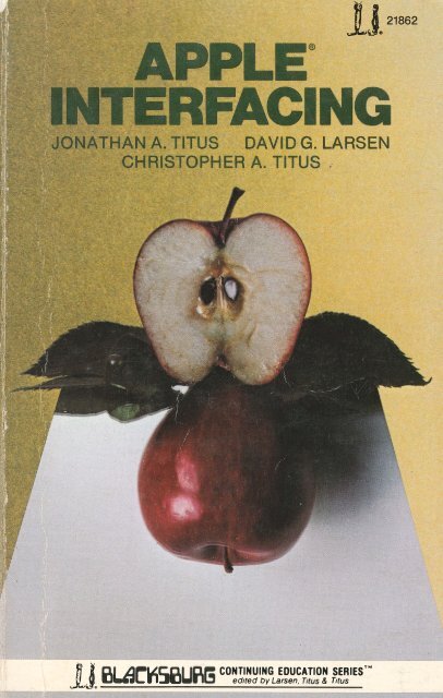
lJ. 21862<br />
APPLE®<br />
INTERFACING<br />
JONATHAN A. TITUS DAVI D G. LARSEN<br />
CHRISTOPHER A. TITUS ,.<br />
lj DI .ll,_ILC:.DUDP.! CONTINUING EDUCATION SERIES"'<br />
IJWllL.11.:Jll 11 edited by Larsen, Titus & Titus<br />
.
Tha Blacksburg Continuing Educ"lk;n SeriesTM of books prnvide " lciborntory-or experimenlo:idented<br />
approach la eledronic lopico. l'resen·r and forthcoming !i!les in !his series i11dude:<br />
® Advanced 6502 lnterfodng<br />
@ Analog I nsl'rumenh:ltio11 Fundcmumtols<br />
G Apple I 11terfodng<br />
$ Basic Busines,s SoHwal'e<br />
"' BASIC Programmer's Notebook<br />
"' Circuit Design Programs for the Apple II<br />
© Circuit Design Programs for the TRS-80<br />
'ii Dedgn of Active filters, With hperimenh<br />
® Design of OpAmp CircuHsf V/Hh Experimenfa<br />
® Design of Phase-lodrncl loop Circuits, Wilh Experiments<br />
@ Design of Trcmsisior Circuitsf Vv'Hh Expedm@mis<br />
Design of VMOS Circuits, Wit!i Experimen·rs<br />
® 80SO/ll085 Soflwarn Design (2 Volumes)<br />
"' S085A CookbMk<br />
e Eledronic Music Circuits<br />
'1l 555 Time,· ApplicoHons Soureebook, With Expecim&nls<br />
9 Guide lo CMOS Basics, Circuit•, & Experiments<br />
8 How lo Program and lnlerfoce the 6800<br />
"' Introduction lo f-ORTH<br />
® f.Aicroeomputer-Analog Converter So Hwa re and Hardware I nterfaeing<br />
1:i> Microcompu!&r lnlerfodng Willi the 8255 Pl'I Chip<br />
@ fv\icrocomputer Design and Mcdnlencrnce<br />
" NCR Basic Eledreinies Course, With E::periments<br />
® NCR Data Ccmmunkotion Corie:epts<br />
9 NCR Data Precessing Concepts Course<br />
APPLE®<br />
INTERFACING<br />
by<br />
Jonathan A. Titus, David G. Larsen, and<br />
Christopher A. Titus<br />
Howard W. Sams & Co.; Inc.<br />
4300 WEST 62ND ST. INDIANAPOLIS, INDIANA 46268 USA
Copyright© <strong>1981</strong> by Jonathan A. Titus, Christopher A.<br />
Titus, and David G. Larsen<br />
FIRST EDITION<br />
SECOND PflINTING-1982<br />
AH rights reserved. No part of this book shall be<br />
Ho1uHJu11'""u. stored in a retrieval system, or transmitted<br />
any means, electronic, mechanical, photocopying,<br />
recording, or otherwise, without written permission<br />
from the publisher. No patent liability is assumed with<br />
respect to the use of the information contained herein.<br />
'Nhile every precaution has been taken in the<br />
preparation of this book, the publisher assumes no<br />
for errors or omissions. Neither is any<br />
liability assmned for damages resulting from the use<br />
of the info1·mation contained herein.<br />
International Standard Book Number: 0-672-21862-3<br />
Library of Congress Catalog Card Number: 81-84282<br />
Edited by: Bob Manville<br />
1llustrated by: Jill E. Martin<br />
Printed in the United States of America.
Preface<br />
The purpose in writing this book is to introduce you to the signals<br />
within the Apple®"' II computer and to show you how these signals<br />
can be used to control external devices under the control of BASIClanguage<br />
programs. A general-purpose computer interface breadboard<br />
has been developed to speed your circuit design and testing<br />
so that you can easily perform the many interesting experiments that<br />
are included in the book. By using a design system such as the one<br />
described in this book, you will spend your time concentrating on<br />
the ·principles involved, rather than troubleshooting your circuits.<br />
However, you will have the opportunity to build and test many digital<br />
circuits, as well as circuits that use digital-to-analog and analogto-digital<br />
converters.<br />
We have chosen to use the Apple II computer with 16K of read/<br />
write memory, and the Applesoftt BASIC interpreter program.<br />
This software provides a great deal of flexibility and it is worth having<br />
it available when you are using external interface circuits. The<br />
Applesoft BASIC interpreter has two general-purpose commands<br />
that can be used to transfer information to and from the computer.<br />
These instructions are easily mastered, without requiring a detailed<br />
understanding of the 6502 microprocessor integrated circuit (IC)<br />
that is used as the "heart" of the Apple.<br />
First we will introduce you to the control signals that are available<br />
from the Apple computer for <strong>interfacing</strong>, and we will show you how<br />
they are used. Some of the signals will not be described, since they<br />
are generally not used in interface circuits, and are meant to be used<br />
by special interface devices that are manufactured commercially.<br />
Our next step is to show you how the Apple can identify or address<br />
external devices through the use of two general-purpose instructions,<br />
PEEK and POKE. These commands are central to the control of external<br />
devices; we spend some time covering their operation and the<br />
use of a variety of circuits that can be used to identify specific input/<br />
output, or I/O devices. You will also see how the Apple can transfer<br />
information to and from external devices over the bidirectional data<br />
"Apple and Apple II are registered trademarks of Apple Computer, Inc.<br />
f Applesoft is a trademark of Apple Computer, Inc.
us; the basic circuits used for input ports and output ports are described<br />
in detaiL Real circuits are provided, so that you can quickly<br />
use the many examples in designing your own interface devices.<br />
You will also see the power of BASIC-language programs-as the<br />
data is processed within the computer to provide meaningful results.<br />
Simple control programs are provided to show you how BASIC-language<br />
programs and I/0 devices can interact. You will be able to<br />
write simple control and data processing programs to go along with<br />
your I/0 ports and devices.<br />
Since the computer is not always synchronized to external devices,<br />
there must be some interaction between the computer and the various<br />
I/ 0 devices so that each knows when the other is ready for some<br />
appropriate action. This leads us to the topic of flags-those signals<br />
that are used by the computer and by external I/0 devices to allow<br />
information to be transferred in an orderly fashion. Since flags are<br />
important, we spend some time on them and on the corresponding<br />
circuits that are actually used in external devices. Software is covered<br />
too, since the flag circuits are useless unless they can be sensed by a<br />
control program.<br />
We have assumed that you have a fairly good understanding of the<br />
commands in Applesoft BASIC. If you are just getting started with<br />
the Apple computer, we hope that you will take some time to review<br />
the simple commands, such as FOR, GOTO, IF ... THEN, PRINT,<br />
and INPUT. Other commands will be introduced in the text and experiments,<br />
and we will provide the details of their operation. At the<br />
end of this book, the use of these and other commands should be<br />
second-nature.<br />
In Chapter 6, we have provided 16 detailed, step-by-step experiments<br />
that you can perform to reinforce the many <strong>interfacing</strong> principles<br />
that have been developed in the text. You will also see the<br />
power of BASIC-language programs for interface control and for<br />
actually processing the information that is involved in transfers to<br />
and from I/ 0 devices. We have made an effort to cover a broad spectrum<br />
of interesting interface applications. Throughout the experiments,<br />
you will see that the same basic principles apply to all of the<br />
interface circuits, from the simplest to the most complex.<br />
We realize that it is difficult to write a book like this for an audience<br />
that has a wide range of backgrounds, from the beginner to the<br />
advanced user, Thus, we have chosen to start at some middle point.<br />
We have chosen to skip basic binary numbering, decimal-to-binary<br />
conversions, basic digital electronics, and breadboarding. These topics<br />
are covered in detail in other books, and the reader who is in the<br />
middle of our assumed spectrum of readers probably has a good<br />
understanding of these topics. In some places, a paragraph or two of<br />
review material have been provided, just to serve as a refresher. Vve
make no attempt to provide much detail here, simply enough to get<br />
you started.<br />
We have assumed some familiarity with SN7400-family digital integrated<br />
circuits, or chips, such as the SN7 402 quad NOR gate and the<br />
SN7475 quad latch chip. Other complex chips will be introduced and<br />
explained in sufficient detail so that you can use them as shown in<br />
the text or experiments. If you wish to use these devices in other<br />
applications, we suggest that you obtain the necessary data sheets<br />
from the manufacturers. The data sheets will provide the necessary<br />
information for a wide variety of uses, and they will also reflect any<br />
basic changes or modifications that may have been made to an "updated"<br />
device, or one that has been "enhanced" with some special<br />
feature.<br />
The Apple II computer has eight general-purpose 50-conductor<br />
interface connectors in its case. The basic bus signals used in the experiments<br />
are derived from the signals at these connectors, so if you<br />
decide to design and build some of your own interface circuits that<br />
will be plugged into one of these "slots," you will find the same signals<br />
are readily available at the edge connectors. However, there are<br />
also some special-purpose signals that are generated by the Apple to<br />
make the <strong>interfacing</strong> task somewhat easier. These signals and their<br />
uses are described in detail in Chapter 7. Since the signals are not<br />
general purpose, but are specific to the Apple, and in many cases,<br />
specific to a particular connector, they are described last. To show<br />
you how these signals are used, a simple asynchronous-serial communication<br />
interface circuit is described, and software to control it<br />
is listed. This type of interface can be used to communicate with<br />
other computers, serial printers, modems, and other interface devices<br />
that use the asynchronous-serial data format.<br />
We have not described assembly-language programming, since<br />
this is a specialized topic and requires a great deal of background.<br />
However, we have provided one simple assembly-language subroutine<br />
for you to use in several of the experiments. There is a good<br />
reason for including this subroutine; the equivalent function is not<br />
readily available in Applesoft. The function required is the logical<br />
ANDing of 8-bit bytes. The logical AND in Applesoft is simply a trueor-false<br />
AND operation, and it cannot be easily used for bit ANDing.<br />
The assembly-language subroutine also provides you with an introduction<br />
to how such routines can be accessed by a BASIC-language<br />
program. We have chosen to use the more complicated USR (X)<br />
command, rather than the CALL command, since we think that<br />
more will be learned.<br />
We found that there were some limitations to the Apple. For example,<br />
there is no simple "rounding" command that can be used to<br />
round a number to a specific number of decimal digits, for example
4.1986 to 4.20. Likewise, the absence of a bit-by-bit ANDing command<br />
was a limitation that was overcome with an assembly-language routine.<br />
We also found that the potentially useful WAIT command that<br />
is used to test individual bits will "hang up" the computer if the condition<br />
is not found. The computer continues to wait if the condition<br />
is not met, and you must reset the computer to get your program<br />
going again. A color display and nice graphics are available, although<br />
we used a black/white monitor in our system.<br />
Most of the special purpose chips, such as the analog converters,<br />
have been chosen because of their simplicity, low cost, and availability.<br />
This is not meant to be an endorsement of these products. As<br />
your <strong>interfacing</strong> sophistication increases, you will find other specialpurpose<br />
devices that can serve the same function, but perhaps with<br />
added features, more resolution, different power supplies, etc. Our<br />
aim is to get you started, and not to provide you with a sourcebook<br />
of every possible interface to the Apple computer system. An impossible<br />
task in any case.<br />
If you are interested in some additional reading about more advanced<br />
topics, we recommend:<br />
6502 Software Design ( 21656).<br />
Programming & Interfacing the 6502, With Experiments ( 21651).<br />
Microcomputer-Analog Converter Soware and Hardware Interfacing<br />
( 21540) .<br />
We also recommend TRS-80 Interfacing, Book 2. While written<br />
around the TRS-80 computer, this book details more advanced <strong>interfacing</strong><br />
topics such as driving high-current/high-voltage loads, serial<br />
communications, remote control, analog converters, filtering and<br />
data processing, and other interesting topics. You will quickly see<br />
that the similarities between the TRS-80 and Apple are much greater<br />
than their differences. Control signals and BASIC commands are almost<br />
identical. All of the books noted above are available from<br />
Howard W. Sams & Co., Inc., 4300 West 62nd Street, Indianapolis,<br />
IN 46268"<br />
The pin configuration figures used in most of the figures, unless<br />
otherwise noted, are provided through the courtesy of Texas Instruments,<br />
Incorporated. The names Apple and Applesoft are trademarks<br />
of Apple Computer, Inc., Cupertino, CA The name TRS-80<br />
is a registered trademark of Radio Shack.<br />
We hope that you enjoy this book, and that it leads you to design<br />
and build some interface circuits of your own.<br />
JONATHAN A. TITUS, C:aRISTOPHER A. Trrus and DAVID G. LARSEN<br />
"The Blacksburg Group"
Contents<br />
CHAPTER 1<br />
6502 PROCESSOR<br />
9<br />
Memory-Input/Output ( 1/0) Devices-Software 1/0 Control Instructions<br />
CHAPTER 2<br />
APPLE INTERFACING .<br />
26<br />
1/0 Device Address Decoding-Device Addressing<br />
CHAPTER 3<br />
1/0 DEVICE INTERFACING .<br />
44<br />
Output Ports-Input Ports<br />
CHAPTER 4<br />
FLAGS AND DECISIONS .<br />
57<br />
1/0 Device Synchronization-Logical Operations and Flags-Flag<br />
Detecting Software-Assembly-Language Logical Operations-Complex<br />
Flags-Flag Circuits-Multiple Flags-Interrupts-Final Words<br />
CHAPTER S<br />
BREADBOARDING WITH TIIE APPLE<br />
69<br />
Basic Breadboard-Connections to the Apple-Other Considerations
CHAPTER 6<br />
APPLE INTERFACE EXPERIMENTS .<br />
86<br />
Introduction to the Experiments-Use of the Logic Probe-Use of the<br />
Device Address Decoder-Using Device Select Pulses-Constructing<br />
an Input Port-Multibyte Input Ports-Input Port Applications-Input<br />
Port Applications (11)-Constructing an Output Port-Output<br />
Port and Input Port Interactions-Data Logging and Display-Simple<br />
Digital-to-Analog Converter-Output Ports, BCD and Binary Codes<br />
-Output Ports Traffic Light Controller-Logic-Device Tester-Simple<br />
Flag Circuits-A Simple Analog-to-Digital Converter<br />
CHAPTER 7<br />
ON THE Bus . 164<br />
Interface Control Signals-An Interfacing Example<br />
APPENDIX A<br />
LOGIC FUNCTIONS • .<br />
180<br />
APPENDIX B<br />
PARTS REQUIBED FOR THE EXPERIMENTS . 183<br />
APPENDIX C<br />
6502 MICROPROCESSOR TECHNICAL DATA . 185<br />
APPENDIX D<br />
APPLE INTERFACE BREADBOARD p ARTS . . 195<br />
APPENDIX E<br />
PRINTED-Cmcurr BoARD ARTWORK . . 197<br />
INDEX . 203
CHAPTER 1<br />
6502 Processor<br />
The Apple II® (Apple®) computer system by Apple Computer,<br />
Inc., uses the 6502-type of microprocessor integrated circuit. This<br />
"chip" forms the heart of the central processing unit (CPU) of the<br />
computer, the place where the actual mathematical, logical, decisionmaking,<br />
and other operations take place. The 6502-type microprocessor<br />
chip is manufactured by MOS Technology (Norristown, PA<br />
19401) , Rockwell International (Anaheim, CA 92803) and Synertek<br />
Corporation (Santa Clara, CA 95051) .<br />
The 6502 is an 8-bit processor. 'Oius, all of the mathematical, logical,<br />
data transfer, input and output operations operate on eight<br />
binary bits at a time. Each bit, of course, can be either a logic one<br />
or a logic zero. The 6502 uses an 8-bit data bus to transfer information<br />
between itself and various memory locations and input/ output<br />
(I/ 0) devices such as a keyboard, printer, etc. In cases where the<br />
value of the information exceeds the limit of eight bits, multiples of<br />
8-bit data words are used. Each 8-bit data word is generally referred<br />
to as a byte.<br />
You should realize that the maximum value that can be expressed<br />
with eight bits is lllllllh or 25510• If larger values are to be operated<br />
on in an 8-bit computer system, then multibyte operations are<br />
required. Generally, this means that corresponding data bytes in two<br />
data words are operated on, followed by the operation being performed<br />
on the next corresponding set of bytes in the. large data<br />
words. In this way large values, beyond the value of 255, may be<br />
readily processed. It is important to remember, though, that the<br />
Apple and App _<br />
le II are registered trademarks of Apple Computer, Inc.<br />
9
Apple CPU can only process and transfer eight bits or one byte at a<br />
time.<br />
The 6502 uses a single set of eight pins to make the connection<br />
with the data bus in the computer. This data bus is used to transfer<br />
information both to and from the computer. This type of a bus is<br />
called bidirectional, since it allows information to flow in two different<br />
directions. This is much like a highway that is used to allow<br />
vehicles to drive one way in the morning and to allow vehicles to<br />
travel in the opposite direction in the evening.<br />
The 6502 generates control signals on the integrated circuit that<br />
are used both internally and externally to supervise and manage the<br />
flow of information on the bus, in one direction at a time. VV e will<br />
explore the generation and use of these signals later in this book.<br />
All computer systems have some memory associated with them. In<br />
general, the memory is used to store both a program that will control<br />
the operation of the computer, as well as the information that is to<br />
be processed. In the 6502 computer, each memory location can be<br />
used to store eight bits of information, or one byte of data. Most<br />
memories consist of multiples of these one-byte storage locations,<br />
generally in multiples of 1024, abbreviated lK.<br />
The memory locations must be addressed in some way so that the<br />
computer knows exactly where it is to store data or obtain program<br />
step information. The 6502 microprocessor chip has 16 address outallowing<br />
it to specify any one of 216 or 65,536 memory locations,<br />
each of which can contain one byte. This is often shortened to 64K,<br />
indicating that 64K bytes of information can be addressed. In almost<br />
all microcomputer memory systems, each memory location is<br />
uniquely addressed with a 16-bit address.<br />
The address bus lines are labeled AO through Al5, corresponding<br />
to the least-significant bit (LSB) through i:he most-significant bit<br />
( MSB), respectively. The LSB and MSB can both be either a logic<br />
one or a logic zero, but their position gives the LSB a value of zero<br />
or one and the MSB a value of zero or 32,768. Since the 6502 is an<br />
8-bit processor, the address lines are frequently<br />
of eight lines each, A7-AO and Al5-A8. The lines are referred<br />
to as the low or LO address, while lines Al5-A8 are referred to as the<br />
high or HI address. In many 6502-based computers, the HI address<br />
is also called the page since the memory may be<br />
divided into 256 pages, with 256 bytes per page. The uses of the<br />
dress bus will be explored further when software i:nsh·uctions are disand<br />
when interface circuits<br />
Unlike the data
Fig. 1- 1. 6502 Microprocessor chip<br />
pin configuration.<br />
vss 1 40 RES<br />
ROY 2 39 2(0UT)<br />
1(0UT) 3 38 s.o.<br />
IRQ 4 37 o(IN)<br />
N.C. 5 36 N.C.<br />
NMI 6 35 N.C.<br />
SYNC 7 34 RtW<br />
vcc 8 33 DO<br />
AO 9 32 01<br />
Al 10 31 02<br />
A2 11 30 03<br />
A3 12 29 04<br />
A 4 13 28 05<br />
AS 14 27 06<br />
A6 15 26 07<br />
A7 16 25 A15<br />
A8 17 24 A14<br />
A9 18 23 A13<br />
AlO 19 22 A12<br />
All 20 21 vss<br />
in only one direction, from the CPU to the memory and to external<br />
devices.<br />
The pin configuration of the 6502 is shown in Fig. 1-1. Although<br />
most of the other signals may be meaningless to you now, you should<br />
be able to identify the 8 data bus input/ output pins and the 16<br />
address output pins.<br />
Since the memory section is being discussed, there are two basic<br />
types of memory devices used in microcomputer systems. They are:<br />
1. Read/Write-Read/Write (R/W) memory is used for the storage<br />
of data that will be changed or updated. The computer<br />
must be able to place the information in a memory location and<br />
then be able to read it back. Programs that will change are also<br />
stored in R/W memory for the same reason. The lowest cost<br />
Apple computer contains 16,384 or 16K bytes of R/W memory.<br />
2. Read-Only-Read-only memory (ROM) is used when data values<br />
and program steps will not be altered. The BASIC interpreter<br />
program in your Apple system is contained in read-only<br />
memory chips. The Apple BASIC interpreter is stored in 12K<br />
of ROM.<br />
There are various sub-classes of these types of memory devices.<br />
The R/W memories may be either static or dynamic. Static memory<br />
chips will maintain the values stored in them until they are changed.<br />
Dynamic memories require refreshing by external hardware every<br />
few milliseconds or they will "forget" or lose the data stored in<br />
them. The R/W memories in the Apple are dynamic, with the neces-<br />
11
sary refreshing circuitry contained on the computer printed-circuit<br />
board.<br />
There are many types of read-only memories. The various types<br />
are generally all static, the differences occurring in the means of storing<br />
the 8-bit values in the memory locations. The two most important<br />
types are mask-programmed and field-programmed. The mask-programmed<br />
devices have data values, program steps, etc., stored in<br />
them during the various manufacturing steps. They are generally referred<br />
to as ROMs. The field-programmable devices require some<br />
kind of special programming circuitry to store the logic ones and<br />
zeros in the various locations. Some of the field programmable<br />
ROMs, or PROMs, as they are generally called, can be erased under<br />
high-intensity ultraviolet light. They can then be reprogrammed.<br />
This is very useful when programs are being developed that will be<br />
stored in read-only memory. It does not require the development of<br />
masks and chips-an expensive process-each time a program bug is<br />
found or a change is made.<br />
A few final words are required about semiconductor memory devices.<br />
The read-write devices are volatile, since data (your program<br />
and values) will "evaporate" or disappear when power is removed<br />
from the system. The read-only memories, on the other hand, are<br />
considered to be nonvolatile, since they will maintain the data or<br />
program steps (the BASIC interpreter) when the power has been<br />
removed.<br />
Most memory integrated-circuit packages or chips do not have all<br />
16 of the address lines connected to them. They have only enough<br />
address connections to uniquely address the memory locations within<br />
the individual chip. Thus, a 64-byte chip, small by standards of today,<br />
would only have 6 address line inputs while a 1024 ( lK) byte<br />
memory chip would have 10 address line inputs. Memory chips such<br />
as these have an additional control or chip-enable input that allows<br />
banks or groups of the chips to be selected, one set at a time. Various<br />
decoding and selecting circuits may be used, thus allowing a 32K<br />
block of memory to be constructed from 64-byte or lK byte chips,<br />
or even combinations of the two. The main point here is that the<br />
memory chips do not require all 16 address lines to be connected<br />
directly to them, although some combination of all 16 address bits<br />
will be used to uniquely select one byte. You should not be confused<br />
when you are confronted with a lK X 4 bit memory that only has<br />
10 address inputs and a chip enable input. This concept will be developed<br />
further as you study input/ output data transfers.<br />
One control signal is generated by the 6502 processor chip to control<br />
the flow of information on the data bus. This signal is noted as<br />
READ/WRITE, or more simply, R/W. Whenever a read, or a write,<br />
operation is to take place, the 6502 must specify a Hl-bit address to
locate the memory "cell" that is to be involved in the transfer. In this<br />
case, the cell is an 8-bit word or byte.<br />
The "bar" over part of the signal notation indicates that when the<br />
signal is a logic zero, a write operation is taking place; and when in<br />
the logic one state, a read operation is taking place. Thus, a single<br />
line controls all of the memory functions. In some 6502-based computer<br />
systems and peripherals, you may see the signal "split," tovide<br />
two memory control signals, memory read ( MEMR or MR),<br />
and memory write ( MEMW or MW). This takes some additional<br />
gating, so in most cases, the R/W signal is used by itself. It is available<br />
at pin 34 on the 6502 microprocessor chip.<br />
You may also see the notation RAM used to incorrectly signify<br />
read/write memory. The acronym RAM stands for random-access<br />
memory. In fact, all of the modern, easy-to-use memory devices are<br />
random access, since one may address one location and then any<br />
other, without having to sequence through all of the locations between<br />
the two addresses.<br />
Pin configurations for typical memory chips have been provided<br />
in Fig. 1-2.<br />
For additional information about memory devices, we refer you to<br />
• Intel Memory Design Handbook, Intel Corporation, Santa<br />
Clara, CA 95051, 1975.<br />
PIN CONFIGURATION<br />
24<br />
Vee<br />
PIN CONFIGURATION<br />
LOGIC SYMBOL<br />
M2708<br />
As<br />
Ag Ill<br />
Vee<br />
CS/WE<br />
\\Jo<br />
PROGRAM<br />
Os<br />
A s<br />
A5<br />
A4<br />
A3<br />
A o<br />
A1<br />
A 1<br />
cs<br />
GND<br />
A<br />
1 18 Vee<br />
o<br />
A1<br />
2 17 A i 1101<br />
A<br />
3 16 z<br />
A s<br />
A3<br />
4 2114 15 Ag<br />
A4<br />
1102<br />
5 14 1101<br />
6 13 1102<br />
A 1/03<br />
7 12 1/03<br />
s<br />
A<br />
8 11 1/04<br />
i<br />
A<br />
1/04<br />
9 10 WE<br />
s<br />
cs<br />
A5<br />
A 9 WE<br />
05<br />
04<br />
03<br />
A o -A 9<br />
PIN NAMES<br />
ADDRESS INPUTS<br />
Vee POWER (+5V)<br />
PIN NAMES<br />
Ao·A9 ADDRESS INPUTS<br />
01-0e DATA OUTPUTS/INPUTS<br />
CS/WE CHIP SELECT/WRITE ENABLE INPUT<br />
WE WRITE ENABLE GND GROUND<br />
cs CHIP SELECT<br />
1101-1/04 DATA INPUT/OUTPUT<br />
Fig. 1·2. Pin configuration for 2708 lK X 8 PROM and 2114 lK X<br />
4 R/W memory.<br />
13
® The 8080A/9080A MOS Microprocessor Handbook, Advanced<br />
Micro Devices, Inc., Sunnyvale, CA 94086, 1977.<br />
® Mostek Memory Products Catalog, Mostek Corporation, Carrollton,<br />
TX 75006, 1977.<br />
© Bipolar and CMOS Memory Data Book, Harris Semiconductor<br />
Prod. Div., Melbourne, FL 32901, 1978.<br />
!NPUU / OIJlPIJT (! / 0) DEVICES<br />
Most microcomputer-based systems are worthless without some<br />
attached I/0 devices. These devices may be standard peripherals,<br />
such as card readers, printers, displays, or they may be sensors, controllers,<br />
and other devices that most people do not normally associate<br />
with computers. The Apple is no exception. It already has several<br />
I/0 devices associated with it: a television display, a cassette recorder,<br />
and a keyboard.<br />
Other I/ 0 devices can be added to your computer. These devices<br />
may be of your own design or they may be standard, commercially<br />
available devices that are compatible with the Apple. These I/ 0<br />
devices are much like the individual memory locations that were discussed<br />
in the previous section. The I/ 0 devices are attached to the<br />
data bus, since data is transferred to them and from them, and they<br />
are also connected to the address bus so that they may be uniquely<br />
addressed by the 6502 microprocessor chip.<br />
A control signal, READ/WRITE or R/W, is used to synchronize<br />
the flow of data to and from the I/O devices. This signal is also used<br />
in 6502-based computer systems to control the flow of information<br />
to and from the memory chips. Thus, there is no differentiation between<br />
memory addresses and I/ 0 device addresses in 6502-based<br />
computers. In computers that are based upon the 8085- or Z-80-type<br />
microprocessor chips, there are different techniques that are used to<br />
address memory and I/0 devices independently. Since only one synchronizing<br />
signal is used to control memory and 1/0 devices, the<br />
Apple's 6502 processor will be either reading or writing at all times.<br />
When the R/W signal is a logic one, the 6502 is reading information<br />
from the data bus. When the R/W signal is a logic zero, the 6502 is<br />
writing data to an external I/ 0 device, or to a memory location. The<br />
"bar" over the W simply means that the write operation takes place<br />
when the R/W signal is a logic zero. You may see other signals with<br />
such bars over their names. This simply means that the signals are<br />
active in the logic zero state.<br />
Since we will be concentrating on the use of I/ 0 devices with the<br />
Apple, we have left a great deal of the specific discussion to the remaining<br />
sections.<br />
l
IR.,view<br />
At this point, you should understand that the 6502 transfers and<br />
operates on eight bits of data at a time. Complex calculations and<br />
operations often require multiple groups of eight bits or bytes. The<br />
bytes are transferred to and from the 6502 CPU on an 8-bit bus.<br />
DATA iii.IS D7-DO An 8-bit bidirectional set of lines for transfer of<br />
information beiween the CPU and I/ 0 devices.<br />
A15-A8<br />
A7-AO<br />
Al1.)DR&:!iS i'IUS A15-AO A 16-bit unidirectional address bus used to address<br />
both memory and 1/0 devices.<br />
HI address bus, most-sig nifkan1 eight address<br />
bits.<br />
LO address bus, least-significant eight address<br />
bits.<br />
cmn11.o !ilGNAi R/W Read/write control signal.<br />
NOTES: The "bar" notation, i.e., W, indicates a iogic zero is the "'active°' state, the state that<br />
causes the corresponding action to take place.<br />
In each case in which a signal is enumerated1 the numbers increase as the signiflcance of the<br />
bits increases, i.e., A 15 == most-significant address bit (MSB).<br />
The 6502 uses a 16-bit address bus to address individual memory<br />
location and I/ 0 devices. The address bus is frequently broken into<br />
a HI and LO address bus, of eight bits each. Th single control signal,<br />
R/W, controlls the flow of information to and from the 6502 CPU,<br />
The signals and their designations are noted in Table 1-1.<br />
C@mm@nd;;<br />
sonw P,RE ! I 0 CONTROIL ifi%]STRIJCT!OIMS<br />
The Apple computer has a number of instructions that are used to<br />
control I/0 devices. For the most part, though, these instructions are<br />
used to control specific I/0 devices or to perform functions.<br />
Without realizing it, you are already familiar some, if not all,<br />
of these I/ 0 instructions.<br />
Here are some specific examples of these I/ 0 control instructions,<br />
to refresh your memory.<br />
The INPUT and PRINT commands are probably familiar to<br />
The INPUT command causes a BASIC program to stop and wait<br />
an input from the keyboard. The PRINT command causes an answer<br />
or string of characters to be "printed" on the tv screen.<br />
10 INPUT "VALUE OF )( IS"; )(<br />
20 PRINT " INPUT VALUE WAS"; X<br />
bampie 1-1. A Simpie l{O '"'!!l'"'<br />
15
If you executed the program in Example 1-1, the value associated<br />
with the variable, X, would have to be entered into the computer<br />
before the program passed control to statement 20. These two types<br />
of I/ 0 statements are frequently used to allow an operator to enter<br />
a value and to see it displayed. There are many variations of both the<br />
INPUT and PRINT commands, but these two examples serve to illustrate<br />
the point; you have already been using If 0 operations in<br />
BASIC-language programs without difficulty.<br />
You may have already discovered that there are also graphic disp"lay<br />
I/O commands in BASIC, too. These are commands such as<br />
HOME, PLOT X,Y and SCRN (X,Y) . The HOME command clears<br />
the screen, and places the blinking cursor at the "home" position in<br />
the upper left-hand corner of the tv screen. The PLOT and SCRN<br />
commands require the use of "coordinates" to indicate where an<br />
operation is to take place.<br />
The program in Example 1-2 shows how some simple graphic display<br />
commands are used in a short program. This program generates<br />
a display of randomly changing colored dots on the tv screen. If you<br />
are using a black-and-white (b/w) tv, you will see the dots in varying<br />
shades of gray.<br />
10 GR<br />
20 X=INT(40*RND(1)) + 1<br />
30 Y=INT(40*RND(1}) + 1<br />
40 COLOR=INT(15*RND(1}) + 1<br />
50 PLOT X,Y<br />
60 GOTO 20<br />
There are two other commands that you may not have considered<br />
to be I/0 commands. These are the LOAD and SAVE commands<br />
that a:re used to read and store programs on cassette tapes. Each<br />
command causes a preset series of operations to take place, controlling<br />
the cassette recorder. The use of these commands is fairly obvious,<br />
so we will not provide an example.<br />
Other I/0 commands are the IN#X and PR#X operations that are<br />
associated with special I/ 0 devices that can be substituted for the<br />
keyboard and tv display. It is important that you realize that these<br />
I/0 instructions are specific to the Apple computer and its BASIClanguage<br />
interpreter program. These instructions would be meaningless<br />
l:o other 6502-based computer systems, unless they used the<br />
Apple BASIC program. The instructions are also specific to one I/ 0<br />
device, i.e., the HOME command will not have an effect on the cassette<br />
recorder, or any other I/0 device. Likewise, the INPUT command<br />
controls the input of values only from the keyboard on the<br />
console.
Gei'!eral-fi!Jrp@S('; I/ 0 Commaru:li:><br />
Although there are some general-purpose I/0 commands in the<br />
INTEGER BASIC interpreter program for the Apple computer, for<br />
this book we have chosen to use what we consider to be the more<br />
flexible APPLESOFT BASIC interpreter program If you wish to<br />
convert your Apple computer to this program, a local Apple computer<br />
dealer can assist you.<br />
The two If 0 device commands are PEEK and POKE. They are<br />
used to transfer data to an external device from the computer<br />
(POKE), and to the computer from an external device (PEEK).<br />
There is a specific format for these instrnctions that must be used if<br />
the instructions are to operate properly.<br />
Input and output devices will be referred to as ports. Thus, an output<br />
device will be an output port and an input device will be an inport.<br />
This is standard nomenclature used throughout the microcomputer<br />
industry.<br />
The output instruction, POKE, must specify the address of the<br />
I/0 device that is to be involved in the transfer of data and also the<br />
value that is to be transferred to the addressed device. The actual<br />
format for the POKE instruction is POKE, x,y, where the x value<br />
represents the decimal address of the output device that is to receive<br />
the data value, y. The data, y, must also be a decimal number. Since<br />
the 6502 microprocessor chip can address 65536 memory locations,<br />
the address must be within the range of 0 to 65535, inclusive. The<br />
data value must be within the range of 0 to 255, inclusive, since the<br />
computer uses an 8-bit data bus for all data transfers, and the largest<br />
number that can be transferred on such a bus is 255.<br />
The value 215 is sent to output port 12684 in the following statement:<br />
POKE 12684,215.<br />
The input instruction, PEEK, is similar to the POKE instruction,<br />
except that no data value is incorporated into the command. VVe are<br />
interested in determining the value present at the specific input device,<br />
so only the decimal address of the input device is specified;<br />
PEEK ( x), where x is the decimal address of the input device.<br />
It does little good to input a value without doing something with<br />
it, so the input command is always incorporated in a complete statement,<br />
rather than being a statement by itself. An example of this is<br />
Q= PEEK ( 34579) .<br />
In this case, the variable, Q, is assigned the decimal value that has<br />
been input from device 34579. It is important that you remember to<br />
enclose the address of the input device in parentheses.<br />
Whenever a PEEK command is used, the value that is input will be<br />
between 0 and 255, :inclusive. Again, this is due to the limitation of<br />
8-bit transfers.<br />
l )'
POKE 45124,98<br />
POKE N,120<br />
POKE 45124,X<br />
POKE X,M<br />
l = PEEK (23109)<br />
l = PEEK (Q)<br />
The input and output commands may have variables specified<br />
within them, rather than specific values for port addresses, and in the<br />
case of the POKE command, data values. Thus, all of the PEEK and<br />
POKE commands shown in Table 1-2 are valid. We have assumed,<br />
of course, that the values for the variables, N, M, X and Q have been<br />
specified somewhere in the program prior to the use of the instructions<br />
shown in Table 1-2.<br />
Input and output commands in which the address values exceed<br />
65535 will generate an ILLEGAL QUANTITY ERROR in the Apple<br />
computer. An attempt to output a numerical data value that exceeds<br />
255 will also generate an ILLEGAL QUANTITY ERROR.<br />
We have provided some examples that show the use of the POKE<br />
and PEEK commands. 'While the programs shown in Example 1-3<br />
can be executed, they will not do anything useful, since you do not<br />
have any external I/0 connected to your computer, at present.<br />
hample 1·3. 5imple D/O l'rnsrnm• for li'El"K mu! OK Commailcl•<br />
10 lf\IPUT "OUTPUT PORT # =";P<br />
20 lf\IPUT "VALUE FOR OUTPUT"; V<br />
30 POKE P,V<br />
40 GOTO 10<br />
10 lf\IPUT "INPUT PORT # = "; M<br />
20 _ PRl1'1T "VALUE AT PORT ="; PEEK-(M),<br />
30 GOTO 10<br />
Since 6502-based computers cannot<br />
between memory<br />
locations that are used for the temporary storage of programs and<br />
data, and those that are being used for I/ 0 ports, the PEEK and<br />
POKE instructions are frequently used to examine and alter the contents<br />
of various memory locations within the Apple. If you POKE<br />
information into read/write memory in an indiscriminate fashion,<br />
you may "write over" important parts of your program, or information<br />
that has been tempornrily stored by the BASIC interpreter. The<br />
net effect is a "crash" of the computer system, in which your program<br />
and data 'Nill be lost or significantly altered. It is probably not a good<br />
idea to randomly POKE information into various addresses, until<br />
some specific guidelines are provided. Of course, you can use the<br />
PEEK command to examine the contents of a memory location<br />
v1henever you since this command will not alter the contents
of an examined memory location. From the previous discussion of<br />
memory devices, you should realize that the POKE operation will<br />
have no effect on the read-only memory devices in the Apple.<br />
Memory Maps<br />
At this point it is a good idea to take a look at the "maps" of the<br />
memory addresses that are used by the Apple. A complete 64K memory<br />
map is shown in Fig. 1-3. For the sake of convenience, the memory<br />
addresses are provided in both decimal (base-10) and hexadecimal<br />
(base-16) notation. The hexadecimal numbers have a suffix of<br />
"H'' to distinguish them from the decimal numbers.<br />
The memory space for the Apple computer has been divided into<br />
four 16K blocks. Three of the blocks have been assigned for R/W<br />
memory, and most Apple computers have the R/W #1 block "filled"<br />
with read/write memory chips. The remaining R/W blocks may be<br />
used for future expansion of R/W memory, if this is required for particular<br />
applications. In most cases, we have found that 16K of R/W<br />
memory is sufficient. Add-on memory chip kits are available from<br />
many suppliers, and most Apple users can probably add the additional<br />
memory chips to their system without much difficulty.<br />
The remaining 16K block of memory has been set aside for both<br />
ROM and 1/0 port addressing. The system ROMs for the Apple,<br />
which include the BASIC interpreter and the monitor programs, take<br />
up 12K of this space. The remaining 4K space is divided into two 2K<br />
spaces for I/ 0 addressing and future expansion of the Apple. The<br />
I/ 0 block with addresses COOOH to C7FFH, inclusive, is the one<br />
of major importance for <strong>interfacing</strong>, since it has been specifically set<br />
aside for this purpose and it will never be used in Apple computer<br />
systems for any other purpose. Some of the addresses within this 2K<br />
block have been used by the Apple for controlling things such as the<br />
speaker, the keyboard, and the cassette recorder. The actual address<br />
49152 COOOH<br />
0 OOOOH 51199 C7FFH<br />
2K 1/0 #1 /51200 C800H<br />
16K R/W#l<br />
.<br />
16383 3FFFH<br />
2K 110 #2<br />
-<br />
53247 CFFFH<br />
16384 4000H<br />
53243 DOOOH<br />
16K R/W#2<br />
12K SYSTEM ROMS<br />
32767 7FFFH<br />
32768 8000H -65535 FFFFH<br />
16K<br />
49151 BFFFH EXPANDED VIEW OF UPPER 16K<br />
49152 COOOH<br />
65535 FFFFH<br />
16K<br />
Fig. 1-3. 64K Memory map for the Apple computer.<br />
19
assignments are shown in Table 1-3. We refer you to Basic Programming<br />
Reference Manual, and App"le II Reference Manual, for details<br />
on the actual use of these I/0 addresses. These manuals are provided<br />
with the Apple II computer, and are also available from Apple Computer,<br />
Inc., 10260 Bandley Dr., Cupertino, CA 95014.<br />
The remaining 2K block of memory, C800H-CFFFH, has been set<br />
aside for future expansion. You may use this space for additional<br />
read-only memory, if you have long programs that you wish to have<br />
readily available.<br />
Address<br />
F•mdion Decimal* Hexade
will now explore the actions that each of these software commands<br />
causes to take place.<br />
The PEEK and POKE instructions operate in a very similar manner.<br />
In each, an address is specified, requiring 16 bits of information.<br />
During the execution of either instruction, the address information<br />
contained within the command is transferred to external devices<br />
on the address-bus lines, Al5-AO. In this way, the 1/0 device address<br />
is available to all of the devices and circuits that are connected to<br />
these address lines, both memory and I/ 0 devices.<br />
When a POKE instruction is used in a program, the data value is<br />
also output by the 6502 chip, but on the data-bus lines, D7-DO. Once<br />
the data bits and the address bits are "stable" or present on their respective<br />
buses in useable form, the 6502 asserts the READ/WRITE<br />
signal on the control bus. This synchronizes the acquisition of the<br />
data by the I/0 device that was addressed. Of course, external circuitry<br />
is required to "capture" the data, as well as to identify the selected<br />
I/ 0 device and synchronize it with the 6502-based system. A<br />
timing diagram for these signals, as they appear on the 6502 system,<br />
in this case the Apple, is shown in Fig. 1-4. Of course, the POKE<br />
command involves many assembly-language instructions, and the<br />
timing diagram shows what happens only during the time of the<br />
actual data transfer. At this point, we are only concerned with what<br />
the 6502 does during a POKE operation.<br />
When a PEEK instruction is executed, the data is not contained in<br />
the instruction, but is acquired from an external I/0 device. Only<br />
the address is specified. The 16-bit address is placed on the address-<br />
i---Tcvc ----i<br />
01<br />
(APPLE 01)<br />
02<br />
(APPLE 00)<br />
DATA<br />
FROM MPU<br />
Fig. 1-4. Write operation signal relationships. (See Appendix C.)<br />
21
us lines when the PEEK instruction is executed. When the address<br />
information is present, the corresponding I/ 0 device must place its<br />
data on the data bus so that it may be accepted by the 6502 processor.<br />
During a read operation, the R/W signal from the 6502 is a logic<br />
one. Additional circuitry is required here, too, to select the I/ 0 device<br />
and to gate its data onto the data bus. A typical timing diagram<br />
for the PEEK command is shown in Fig. 1-5.<br />
--Tcvc ---;<br />
\ (APPLE 01)<br />
y-<br />
1<br />
I<br />
(APPLE 00)<br />
ADDRESS<br />
FROM MPU<br />
DATA FROM<br />
MEMORY<br />
t----TAcc ---1--T DSU<br />
We will describe shortly some of the circuits that are used for input<br />
and output ports. You have probably realized that while we have<br />
described an I/0 port as one that can either receive data that is output<br />
by the microcomputer or transmit data that is input by the microcomputer,<br />
some I/0 devices may actually contain a number of individual<br />
I/ 0 ports. Industrial controllers, data storage devices (disks,<br />
cassettes), analog converters, and other I/0 devices may have a<br />
number of II 0 ports, since they may require more than eight bits of<br />
information from the computer and they may also need to transfer<br />
more than eight bits of inforn1ation to the computer. In any case,<br />
transfers of data that contain more than eight bits always involve<br />
the transfer of multiple bytes to and from the computer and the individual<br />
8-bit I/O ports" This is important to remember: information<br />
is always transferred eight bits at a time.<br />
Software Commai'ld-D&1ta Tr
transfers will require more than eight bits of information, so multiple<br />
bytes are transferred, one byte at a time.<br />
There are also cases in which the actual value of the data transferred<br />
is meaningless. The bits may be used to represent individual<br />
two-state conditions that are unrelated to the positional values of<br />
the bits. For example, a number of sensors could be connected to the<br />
Apple indicating conditions such as tank empty-or-full, heater on-oroff,<br />
value open-or-closed, and so on. A PEEK command could be<br />
used to input the status of these indicator bits, through an 8-bit input<br />
port. Thus, the value read from this input port might be 100, but the<br />
port is sensing eight individual on or off (logic one or logic zero)<br />
states, so the value of 10010 is meaningless. The individual binary<br />
bits each represent the state of an individual sensor. In this case:<br />
10010 = 011001002<br />
This indicates that three of the sensors are in the logic one state and<br />
five are in the logic zero state.<br />
The POKE and PEEK commands can also be used in a similar<br />
manner to turn a device on or to turn a device off, based upon the<br />
state of the individual bits that have been sensed elsewhere in a control<br />
program. In fact, many of the I/0 addresses used by the Apple<br />
are assigned to simple on/ off devices such as the speaker. Thus, a<br />
simple command:<br />
A =<br />
PEEK(49200)<br />
will generate a 'blip" on the speaker in the Apple. You should understand<br />
that the variable, A, is a "dummy," and its final value is not important,<br />
since the net effect of the simple BASIC statement is to<br />
pulse the speaker once. The speaker control command may be used<br />
in a loop to generate a low buzz from the speaker. This is shown<br />
'<br />
in<br />
kU<br />
l 0 A = PEEK(49200)<br />
20 GOTO 10<br />
Example 1-4. A Simple Speaker Control Program<br />
The important point to remember here is that the PEEK and<br />
POKE instructions are not limited simply to controlling the transfer<br />
of information on the data bus. They may also be used for specific<br />
control functions, such as pulsing a counter, turning on a pump, or<br />
tilting a solar collector.<br />
Assembly Language and BASIC<br />
The BASIC-language programs that you write on your Apple computer<br />
bear very little relationship to the actual instructions that the<br />
6502 microprocessor chip can actually execute. Each of your BASIC<br />
23
statements and commands :is interpreted by the BASIC interpreter<br />
resident within the Apple computer. A programming manual for the<br />
6502 chip, itself, would bear little relationship to the Apple software<br />
manual. The commands are very different.<br />
The 6502 does not have a PRINT command, so it would not perform<br />
the following operation:<br />
PRINT "THIS LOOKS LIKE FUN"<br />
The BASIC interpreter determines that a PRINT operation is to take<br />
place and it then executes a series of assembly language program instructions<br />
that actually place the codes for the alphabetical characters<br />
in the display memory to spell out, "THIS LOOKS LIKE FUN."<br />
The assembly language steps consist of logic ones and zeros that<br />
cause the necessary internal and external 6502 operations to take<br />
place to transfer the message portion of the PRINT command to the<br />
display memory.<br />
While we will not use assembly language programming to any extent<br />
in this book, you should be aware that it is the "base" computer<br />
language that causes the Apple to operate the way that it does.<br />
The PEEK and POKE commands each cause many, many assembly<br />
language commands to be executed to produce the overall effect<br />
of data transfer. Since these BASIC language instructions must be<br />
interpreted, even when used one right after another, or in a loop, the<br />
interpretation software process can be slow. Two programs are<br />
shown in Example 1-5, both of which control the speaker in the<br />
Apple. Each series of program steps does the same thing; generating<br />
a tone on the speaker. Simply by listening to the differences in the<br />
two tones produced, you will be able to appreciate the difference in<br />
the speeds of execution of these programs.<br />
Basic Program<br />
l 0 A = PEEK(49200)<br />
20 GOTO 10<br />
Assembly la"!ii""'9"<br />
GO LOY #$CO<br />
LOOP lDA # $0C<br />
JSR WAIT<br />
LOA SPKR<br />
DEY<br />
BNE LOOP<br />
JMP GO<br />
The assembly language program generates a pleasing, even tone,<br />
while the BASIC program generates a low rumble. The assembly language<br />
program is similar to the one used by the Apple Monitor program<br />
where the internal WAIT subroutine has been used to generate<br />
a delay.<br />
In some cases, assembly language programs have a five-hundred<br />
to one advantage over BASIC programs, although the BASIC pro-
grams are probably easier to write and debug. Assembly language<br />
programming is generally not recommended for the novice.<br />
We will be mentioning assembly language programming very little,<br />
concentrating on the use of BASIC language programming instead.<br />
For further information on 6502 assembly language programming,<br />
we recommend 6502 Software Design and Programming and<br />
Interfacing the 6502, With Experiments (Howard W. Sams & Co.,<br />
Inc., Indianapolis, IN 46268).<br />
Binary and Decimal Numbering<br />
The Apple computer system acquires, processes, and prints decimal<br />
(base-10) numbers. This makes it compatible with the numbering<br />
used by most people today. It would be difficult for us to readily<br />
understand and convert data values that were printed in a nondecimal<br />
format. The data and address lines are directly connected to the<br />
6502 microprocessor chip, so they are binary, having only two statesa<br />
logic one or a logic zero. Thus, when we specify an I/ 0 port address<br />
in a PEEK or POKE command, we must realize that the address<br />
( 0-65535 ) will appear in its binary form on the address bus<br />
(0000000 0000-1111111111111111). You should be able to make<br />
the conversion between decimal and binary, in either direction.<br />
Likewise, the data values transferred to and from the computer<br />
by the PEEK and POKE commands are also specified or acquired as<br />
8-bit binary values, since the data bus is only eight bits "wide." The<br />
8-bit data bus is a function of the data processing capability within<br />
the 6502 chip. It is not a function of the Apple. Thus, we are limited<br />
to 8-bit data transfers. Is this a great limitation Generally not. In<br />
spite of it, the Apple can process a great deal of information, and, as<br />
you will see later, it is easy to interface to 1/0 devices.<br />
One final note on addresses is necessary before leaving this chapter.<br />
The BASIC interpreter in the Apple computer has been set up<br />
to handle both negative and positive addresses. This does,n,ot mean<br />
that there are actually negative addresses in the computer. Can you<br />
imagine negative street numbers The negative numbers are simple<br />
due to the way in which the binary equivalents of the addresses are<br />
stored in the Apple. Thus, the address for the speaker, 49200, is<br />
equivalent to -16336. To avoid confusion, we strongly recommend<br />
the use of the positive addresses. You can easily convert between<br />
negative and positive addresses simply by (a) adding 65536 to a<br />
negative address to yield the positive equivalent, or (b) by subtractir1g<br />
65536 from the positive address to yield the negative equivalent.<br />
Both addresses, 49200 and -16336, generate the same 16-bit address,<br />
but we think that you will agree that negative addresses can seem a<br />
hit abstract and confusing.<br />
25
CHAPTER<br />
Apple Interfacing<br />
At this point, you are probably wondering:<br />
® How does the Apple actually transfer information to<br />
vices<br />
(i:ll How are the I/ 0 devices actually synchronized to the operation<br />
of the computer<br />
How are individual I/O devices selected or identified<br />
®' How do I/ 0 devices place their data on the data bus and how<br />
do they actually receive it from the data bus<br />
These are important questions, since the answers to them will provide<br />
the basis for your understanding of microcomputer <strong>interfacing</strong>,<br />
We will be answering these questions in this and other chapters, 'lVe<br />
will also provide some experiments that will reinforce the concepts<br />
through hands-on experience,<br />
A few examples of digital circuits will be<br />
in this chapter,<br />
We have assumed that you can "read" interpret a circuit<br />
diagram, and that you are familiar with the more common SN7 400-<br />
series transistor-transistor logic (TTL) circuits<br />
Before we can discuss the actual transfer of information between<br />
I/O devices and the computer, we must first understand the circuitry<br />
and the signals that are used to identify or address the individual<br />
I/0 devices. There are many schemes that may be used and we will<br />
examine several of them, It is impossible to show possible<br />
scheme for addressing I/ 0 devices, since modifications be made<br />
to suit special needs.
·when the Apple computer is progrnmmed to perform a data transfer<br />
using either of the general-purpose I/ 0 commands, PEEK or<br />
POKE, certain signals are generated by the 6502 processor to synchronize<br />
the flow of data. At this point, our main concern is the use<br />
of the address bus lines. These are the 16 lines that address individual<br />
memory locations and I/ 0 devices. You should recall that the<br />
PEEK and POKE instructions each contain decimal address information<br />
that is used to identify the addressed memory location or I/0<br />
device. Of course, the Apple computer has no way of distinguishing<br />
between a memory location and an I/ 0 port<br />
DEVICE ADDIUiSSiNG<br />
Each If 0 device that is to be used with the computer must be able<br />
to recognize its own device address. Since the PEEK and POKE<br />
commands use 16-bit addresses, each If 0 device must monitor these<br />
16 address lines, Al5-AO, for the occurrence of its address. There are<br />
three basic schemes that may be used by I/ 0 device circuits to accomplish<br />
the monitoring for a specific address. These are:<br />
® Gating-detecting a specific combination of logic signals.<br />
® Decoding-a more flexible gating scheme in which many addresses<br />
may be detected.<br />
® Comparing-comparing a preset or known address with the address-bus<br />
signals until a match occurs.<br />
Combinations of these three techniques are possible and there are<br />
probably many variations that are possible. We will describe examples<br />
of each of the three basic address decoding schemes.<br />
lBsillilg Gillies for Addre!ls Dee:@ding<br />
In the scheme for decoding device addresses in which individual<br />
gates are used, the address must be known so that the gates can be<br />
properly configured. In this example, we will use the device address<br />
1010100011110llb or 4325510. Since the binary notation is long, and<br />
somewhat cumbersome, you might feel more comfortable with the<br />
hexadecimal equivalent, A8F7H. Since NAND/ AND gates are the predominant<br />
type of gating logic available, we will use these types of<br />
circuits in our logic.<br />
To refresh your memory, the pin configurations for several types<br />
of AND/NAND gates are shown in Fig. 2-1, with the generalized truth<br />
table for a two-input AND gate and an equivalent NAND gate shown<br />
in Table 2-1. Since inverters such as the SN7404 are often found in<br />
device addressing circuits, a pin configuration for this chip has been<br />
included in Fig. 2-1. The truth tables in Table 2-1 also show the function<br />
of an inverter. In all cases, the logic one state is the higher volt-
1A 18 lV 2A 28 2Y GNO<br />
SN7400<br />
SN7404<br />
lA 18 2A 28 2C 2V GND<br />
SN7408<br />
SN7410<br />
SN74H11<br />
1A 18 2A 28 2C 2V GNO<br />
ig. 2-1. hwerer and vari11s AND/NANli:I gate pin configurations.<br />
age ( +2.8 to +5 volts) and the logic zero state is the lower voltage<br />
( 0.0 to 0.8 volt). The NAND gate functions are available with 2, 3, 4,<br />
8, and 13 inputs, while the AND gates are available with 2, 3, or 4<br />
inputs.<br />
Since the unique output state, logic one for an AND gate and logic<br />
zero for a NAND gate, occurs only when all of the inputs to an AND or<br />
a NAND gate are all logic ones, we will have to configure the binary<br />
address 10101000111101112 so that it generated 16 logic ones at the<br />
input to the AND or NAND gate, when it is present on the 16-bit address<br />
bus. You have probably realized that there are no 16-input AND<br />
or NAND gates available commercially, so some other configuration<br />
must be used instead. It is very easy to use a separate 8-input NAND<br />
gate to detect a pattern of binary address bits on the high-address<br />
bus ( Al5-A8), and another 8-input NAND gate to detect a pattern of<br />
binary bits on the low-address bus (A7-AO). Simple inverter func-
Y@bie ::!1. VNth i
1Y lA 18 2Y 2A 28 GNO<br />
4A<br />
4Y<br />
lA 18 lY 2A 26 ZV GNO<br />
Si\17402<br />
SN7432<br />
fig. 2·3. lypica! NOR all'Jd Oil gae IC pin
DECODED OUTPUT<br />
puter systems, the R/W line is used to provide the logic-zero 'INTite<br />
pulse, with the R/vV signal being inverted to generate a separate<br />
read pulse. The two resulting control signals, WRITE (WR) and<br />
READ (RD), are easy to use in interface circuits, since they are active<br />
in the logic zero state. The use of these signals is shown in Fig.<br />
2-6. In this circuit, the output from the 16-bit gating circuit is combined<br />
with RD and WR to provide two signals for I/ 0 port control.<br />
two control signals are a combination of the decoded address<br />
the WRITE pulse, and a combination of the decoded address<br />
and the READ pulse. The resulting pulse from each gate is called an<br />
address select pulse, or a device select pulse. More generally, a deaddress<br />
is gated with a function pulse (RD or WR) to generate<br />
a device select pulse. In the circuit diagram shown in Fig. 2-6, the<br />
RD 49280 pulse could be used to control an input while the<br />
WR 49280 pulse could be used to control an output Note that<br />
the notation for the VVR 49280 pulse does not have a "bar" over it.<br />
FROM HIGH-ADDRESS GATE<br />
I <<br />
DECODEU<br />
J-- OUTPUT<br />
SN74LS32<br />
0<br />
SN74LS30<br />
fi!J. 2·5. l'rn!J•ammab!e gai® Msed for devi
FROM HIGH-ADDRESS GATE<br />
0<br />
A7 <br />
A6<br />
A5<br />
DECODED OUTPUT<br />
49280 = C080H<br />
0<br />
A4<br />
A3<br />
A2<br />
WR<br />
Al<br />
0<br />
AO RD 49280<br />
R/W q----1<br />
i9. 2·"'· llisi"!I ll ""'I WR signals t@ !l"'"""'t" device •eld i>"lses for<br />
clevi
1<br />
1<br />
1<br />
Using Decoders<br />
In many cases, it is easier to use decoder circuits in place of the<br />
gate address detecting circuits, and, in some cases, in place of the<br />
NOR-gate device select circuits, too. Why are decoders so useful<br />
' '.Perhaps it is best to take a look at several types of decoders to see<br />
'.·what they look like and how they operate. As you examine the decoder<br />
circuits, keep in mind that they are simply collections of gates<br />
;that have been "integrated" into an easy-to-use decoder circuit.<br />
· Decoder circuits are generally specified as x-line to y-line decoders,<br />
where x represents the number of binary inputs, say four inputs,<br />
· and where y represents the number of possible outputs, or the num<br />
: ber of different binary states present on the x inputs. Thus, for the<br />
fo<br />
6<br />
u<br />
inp duts,<br />
there would be<br />
1 possible out<br />
d 4 16<br />
d d T<br />
ph ts, . cr ati "ng a 4-line<br />
to<br />
f<br />
d<br />
>J - me eco er or a - to - me eco er. is is, m act, a rea e<br />
· poder circuit, as you will see.<br />
,( Each of the binary inputs has two states, a logic one and a logic<br />
zero. These inputs are independent of one another. The outputs are<br />
:,lso binary, in the sense that they have two possible values, but they<br />
"·/Ue not independent. There will only be one unique output from the<br />
)¥coder, representing the value or "weight" present at the binary in<br />
:puts. In most cases, the unique output state is a logic zero, with the<br />
pther outputs in their logic one state.<br />
A typical decoder integrated circuit is the SN74LS 139. This inteated<br />
circuit actually contains two independent two-line to fourne<br />
decoders, as shown in Fig. 2-7.<br />
The truth table for the SN74LS139 is shown in Table 2-3.<br />
Of course, the truth table applies to both of the decoders within<br />
e SN74LS139 integrated-circuit package, or "chip." Most decoder<br />
:rcuits incorporate an enabling input, so that the decoder may be<br />
;.<br />
'LS139, '5139<br />
DATA<br />
OUTPUTS<br />
Fig. 2-7. SN74LS139 decoder chip schematic diagram and pin configuration.<br />
33
1.,p.,10<br />
().,!pl!!$<br />
Eilable<br />
SeleJ74LS139 decoder package can handle our needs. A<br />
decoder circuit is shown in Fig. 2-8. In this circuit, only two<br />
bits have been decoded, the rest have been ignored. Note that<br />
enable has been grounded so that the outputs of the<br />
will<br />
properly. The added NOR and OR gates generate the<br />
select pulses.<br />
The device select signals have been noted as RD RD Y, and WR<br />
Y, since there is no specific address that will actuate eacho Addresses<br />
01010101 00011101 11110110 and 00000000 11111110<br />
all cause the RD X device select to be generated, if they<br />
RDX<br />
DECODER<br />
\VR Y
used in PEEK commands, for example A=PEEK (21762). This nonabsolute<br />
device addressing results because address bits Al5-A2 have<br />
not been used in the decoding scheme. Nonabsolute addressing<br />
means that there are several addresses that will actuate the selected<br />
device. The circuit shown in Fig. 2-8 will decode four addresses and<br />
thus eight individual devices may be selected, four input devices<br />
and four output devices; additional NOR gates or OR gates are required,<br />
though. In a small system, this may be adequate, although<br />
the decoding scheme does not provide a great deal of flexibility in<br />
allowing the addition of new I/ 0 devices beyond the original eight.<br />
Although this scheme is not very flexible, let's take a closer look at<br />
it, since it allows us to develop two other concepts that can be applied<br />
to other decoder schemes.<br />
In Fig. 2-8, the enable input, "G," of the decoder is simply<br />
grounded, to always enable the decoding action. This input can allow<br />
the decoder to be used for absolute decoding. A gating circuit can be<br />
used to supply an enabling signal to the decoder only when a preset<br />
pattern of address bits, on address lines Al5-A2, is present. You have<br />
already seen the use of multiple-input gating circuits; the circuit in<br />
Fig. 2-5 is a good example. This circuit can be readily adapted to<br />
provide the enable input for a simple decoder. Since the Al and AO<br />
inputs are being used as inputs to the decoder, they are not used as<br />
inputs to the gating circuit that provides the decoder-enabling signal.<br />
A simple example of this is shown in Fig. 2-9. In this circuit, the<br />
ADDRESS ENABLE signal is generated by a gating circuit (Fig.<br />
2-5). In this case, the jumpers associated with the Al and AO address<br />
inputs are simply disconnected.<br />
If we assume that the high-address gating circuit has been preset<br />
for an address bit pattern of 11110000, and that the Al and AO inputs<br />
to the circuit have been disconnected (see Fig. 2-5), then the decoder<br />
shown in Fig. 2-9 will only be enabled for addresses 11110000<br />
01101100 through 11110000 01101111. Thus, in this circuit, the de-<br />
ADDRESS ENABLE INPUT<br />
DECODER<br />
Fig. 2-9. Decoder used for absol..,ie ad
} OUTPUT<br />
DEVICE SELECTS<br />
Al<br />
AO<br />
__ _,,__--11----11 B<br />
--
An alternate approach is to use both of the decoder circuits in the<br />
SN74LS139 chip, using the RD and WR function pulses to enable the<br />
decoders. In this way, the address selection is again nonabsolute, but<br />
the device select gating is performed within the chip. This is shown<br />
in Fig. 2-10. The NOR and OR gates are no longer required for each<br />
device select pulse to be generated. While this circuit may not be<br />
immediately useful, it does illustrate the use of the enable input of<br />
the decoder to generate the device select pulse. The decoder gating<br />
or enabling input may be used for device select pulse generation, or<br />
for absolute decoding. In some cases, it may be used for both.<br />
Large Decoders<br />
functional block diagram and schematics of inputs and outputs<br />
There are additional decoder circuits that will be useful to you in<br />
<strong>interfacing</strong> your Apple computer to external devices. These decodpositive<br />
logic: see function table<br />
FUNCTION TABLE<br />
INPUTS<br />
OUTPUTS<br />
G1 G2 0 C<br />
A<br />
10 11 12 13 1"4 15<br />
H<br />
H<br />
L<br />
'H<br />
H,. high level, L =low level, X =Irrelevant<br />
Fig. 2-12. SN74154 decoder.<br />
37
FUNCTION TABLES<br />
2-LINE-T0-4-LINE DECODER<br />
OR 1-LINE·T0-4-LINE DEMULTIPLEXER<br />
OUTPUTS<br />
SELECT<br />
STROBE<br />
OUTPUTS<br />
ers, depending on the type you choose, may have additional<br />
enable lines, and outputs. Examples are shown in Fig. 2-11 for<br />
SN74LS138 decoder and in Fig. 2-12 for the SN74154 decoder. The<br />
SN75155 decoder has also been included (Fig. 2-13) since it has<br />
ADDRESS<br />
BUS<br />
[ A3<br />
A2<br />
20<br />
21<br />
Al ___<br />
22 -1 B<br />
A0 --- 23 4 A<br />
WR OR RD ---1 9 -1 G2<br />
18<br />
D<br />
c<br />
Gl<br />
+5<br />
24<br />
12<br />
15<br />
14<br />
13<br />
12<br />
11<br />
10<br />
9<br />
8<br />
7<br />
6<br />
5<br />
4<br />
3<br />
2<br />
l<br />
0<br />
SN74154<br />
-U"<br />
16 DEVICE SELECT<br />
PULSES<br />
l'i!lJ. 2·1. $11174154 d@
sections, but the address inputs, A and are comrnon to both of the<br />
decoder sections. Each section of the SN7 4155 has separate control<br />
or enabling inputs.<br />
A large decoder such as the SN74154 4-line to 16-line decoder provides<br />
broad address flexibility. A SrT74154 decoder<br />
may be used to nonabsolutely decode 16 addresses, and when either<br />
WR or is used as one of the enable inputs, the SN75154 may be<br />
to directly generate 16 device select pulses,<br />
the need<br />
for additional gating. This is shown in 2-14.<br />
Additional decoders or gates may be to the basic circuit so<br />
that absolutely decoded device select pulses are<br />
example of this is shown in Fig. 2-15. Either RD or Vv'R signal<br />
may be used to gate or enable the lower decoder, The<br />
have been used to gate together the address selection<br />
upper of the circuit and the address selection<br />
tion from the lower decoder. Thus, the upper nA•-l-icm<br />
circuit is used to "qualify" the outputs from the lower decoder to<br />
make the address selection absolute. In this example, two device<br />
selecl: pulses have been shown. Although this circuit will it is<br />
not particularly useful, since it can be simpli£ed.<br />
/ SN74154<br />
SN7404(ALL)<br />
G2 15<br />
Gl<br />
A7<br />
D<br />
A6<br />
c<br />
A5 B 1<br />
114 A 0<br />
SN74154<br />
WR G2 1< - "<br />
SM7402<br />
Gl<br />
A3<br />
D<br />
A2<br />
Al<br />
B<br />
AO- A ()<br />
OUT ''3"<br />
OUT "O"
Since the SN74154 decoders have two enabling inputs, GI and<br />
the NOR gates shown in Fig. 2-15 may be eliminated by using<br />
second enabling input as the "qualifier" that will enable the decoder.<br />
The use of this type of circuit is shown in Fig. 2-16. In this example,<br />
the lower decoder now has two enabling input signals, the RD control<br />
signal from the computer, and the enabling signal from the up"<br />
per portion of the circuit. You should note that the upper decoder<br />
has both of its enabling inputs used, so that it is enabled only for a<br />
specific pattern of bits on the HI address bus. In this case, gating has<br />
been used to generate the enabling signal for the upper decoder.<br />
A third decoder could be added to this circuit to generate device<br />
select pulses for output devices. The inputs to this additional decoder<br />
would be the same as those to the lower decoder, except - that the WR<br />
signal would be used instead of the RD signal.<br />
Many decoder schemes are possible, and you will have an opporh.mity<br />
to explore the use of decoders in the experiments. The main<br />
point is that the use of decoders simplifies the process of device selection<br />
and gating. Decoders are generally used in situations that require<br />
flexibility and the generation of several device select or device<br />
address signals in proximity to one another.<br />
Al5<br />
Al4<br />
Al3<br />
Al2<br />
All<br />
AlO<br />
A9<br />
A8<br />
A7<br />
A6<br />
A5<br />
A4<br />
/<br />
SN7 404 (ALL)<br />
SN74154<br />
G2 15<br />
GI<br />
D<br />
G 2<br />
B 1<br />
A 0<br />
SN74154<br />
G2 15<br />
iiD --! Gl<br />
A3 --o<br />
A2<br />
Al --1<br />
AO --o<br />
D 3<br />
c 2<br />
B<br />
l<br />
A 0 l<br />
16<br />
INPUT<br />
DEVICE SELEG I<br />
PULSES
fUNCTlON TABLES<br />
COMPARING<br />
CASCADING<br />
INPUTS<br />
INPUTS<br />
A3, 83 A2, 82 Al, Bl AO, SO A>B<br />
A3 > 83 x<br />
....<br />
x<br />
OUTPUTS<br />
A>B A
Al5<br />
lS<br />
Al4 ----1"'"""'3<br />
Al3 ----1<br />
""'1<br />
2<br />
Al2 _____ .._l0 "-1<br />
SN7485<br />
A<br />
+5<br />
All<br />
!S<br />
AlO -----1 "-1<br />
3<br />
A9 ------=-1 =-s<br />
Z<br />
A8 ______<br />
10 '-I<br />
A<br />
B<br />
l<br />
<br />
14 ,...,<br />
11<br />
A7<br />
15<br />
A6 ---13'-:1<br />
AS ----12""""'<br />
A4 ----10__,,<br />
S N<br />
Nr:404 <br />
2 1<br />
A<br />
6<br />
19<br />
G2<br />
18<br />
WR -------
flexible decoding scheme, as shown in Fig, 2-19, The unique "equal<br />
condition" output of the SN7 485 comparators is a logic one, so where<br />
necessary, it has been inverted to provide the enabling signal to a<br />
decoder chip. In this circuit, two additional comparators have been<br />
used so that the device addresses are absolutely decoded. Now, the<br />
outputs of the SN7"1154 decoder are only active when address bits<br />
Al5-A4 match the corresponding logic states that have been preset<br />
at the inputs to the three comparator circuits. In this case, the address<br />
bits must be 11101001 for Al5-A8 and 0000 for A7-A4. Since<br />
the WR function pulse must also be present to enable the decoder,<br />
you should realize that output device address selection signals are<br />
being generated by this circuit, for addresses 59648 through 59655,<br />
or E900H through E907H. Another SN74154 decoder could be added<br />
to this circuit to generate 16 device address selection signals for input<br />
devices, You would need parallel connections between the inputs<br />
of both decoders except that the RD signal would be used in place<br />
of the WR signal.<br />
This completes our discussion of device addressing circuits and<br />
the combinations of device addresses and function pulses to obtain<br />
device select pulses. In future examples, we will expect that you will<br />
recognize the notation WR 54390 as a logic-zero device select pulse,<br />
generated by the proper gating of the WR function pulse and address<br />
54390. In some cases, the actual gating will be shown, but in<br />
most cases, we will assume that you understand the origin of the<br />
signal. While you will probably see many different device addressing<br />
and selecting circuits in other books, magazine articles, etc,, you will<br />
quickly find that they all function in pretty much the same waygating<br />
an address signal with a function pulse to select a particular<br />
device.<br />
In some of the experiments, you will explore the use of device<br />
select pulses to control devices, In the next chapter, you will learn<br />
how these pulses are used to control the flow of 8-bit data bytes on<br />
the data bus of the 6502.
1/0 <strong>interfacing</strong><br />
Now that we have developed a number of ways of selecting<br />
identifying 1/0 devices, the actual construction and configuration<br />
the I/0 ports become very important. In this section, we will<br />
velop some of the actual bus <strong>interfacing</strong> schemes that will allow I/ 0<br />
devices to transfer 8-bit bytes to the computer and to receive bytes<br />
transferred to them by the computer. As we found with the<br />
selecting circuits, there are many circuits for input ports and output<br />
ports. Only a few sample circuits will be provided to illustrate the<br />
basic principles of <strong>interfacing</strong>.<br />
Output ports are devices that receive data bytes from the computer,<br />
controlled by POKE commands in the BASIC-language programs.<br />
You have already seen that there is a definite timing relationship<br />
between data on the bus, the WR pulse and the device address,<br />
when a POKE command is executed. This has been shown in Fig.<br />
1-4. In the Apple computer, the duration of the WR pulse is about<br />
500 nanoseconds. If we use the WR pulse to gate the data from the<br />
data bus to an output device, through the use of the device select<br />
pulse, the data is only presented to the output device for about 500<br />
nanoseconds. This period is hardly long enough to allow the receiving<br />
device to perform a meaningful function. To eliminate this problem,<br />
each output port must be equipped with some sort of circuit<br />
that can acquire data from the bus and "hold" it for as long as<br />
needed, or until it is "updated" by another data transfer.<br />
The type of circuit that can perform this function is called a<br />
since it can latch the information and hold it until it is updated or<br />
44
until the power is turned off. There are many different types cf latch<br />
integrated circuits that offer different configurations of control and<br />
data inputs and outputs. Rather than describe all of the various types<br />
of latches, we have chosen to describe three general-purpose devices,<br />
the SN7475, the SN74175, and the SN74LS373. The pin configurations<br />
and function tables are shown in Fig. 3-L While tb.£Nl::!c7l5<br />
i;.§JI1L.SJ1.X."tr.1!.1l!::t£h .. 9xiy§§, .th N §N7JF§.E!!l:.Sl1 t i l1 s<br />
flir;i«-
ENABLE<br />
1-2 GND<br />
30<br />
JG<br />
FUNCTION TABLE<br />
(Each Latch)<br />
INPUTS<br />
OUTPUTS<br />
0 G 0 0<br />
L H L H<br />
H H H L<br />
x L Oo Go<br />
H =high !evel, L = low level, X ""irrelevant<br />
Oo =the level of Q before the high-to-low transition of<br />
1D 2D ENABLE Vee 30<br />
,_,<br />
'LS373, 'S373<br />
FUNCTION TABLE<br />
OUTPUT<br />
CONTROL<br />
ENABLE<br />
G<br />
D<br />
H<br />
H<br />
H<br />
H<br />
H<br />
L<br />
x<br />
x<br />
x<br />
0.0<br />
z<br />
FUNCTION TABLE<br />
!EACH FLIP-FLOP)<br />
INPUTS<br />
OUTPUTS<br />
CLEAR CLOCK D Q Qt<br />
L x x L H<br />
H t H H L<br />
H t L L H<br />
H L x Oo Go<br />
fig. 3-l. p;., cMlig.,ratio:ms am! famdi" tables for Sl\!7475 [¥op), SN74LS37:'l<br />
(middle), and Sl\!741 75 (bonom) latd-1 chips.<br />
not continuously gated through the SN7 4175 on either the logic zero<br />
or the logic one portion of the clock signal. This is what distinguishes<br />
this flip-flop device from the latch devices, although in computer <strong>interfacing</strong>,<br />
the net effect of both types of chips is the same.<br />
A common clear input is also provided on the SN74175, so that the<br />
flip-flops may be "cleared" ( Q=O, Q=l), when this input is taken to<br />
D<br />
INPUT<br />
G<br />
INPUT<br />
Q<br />
OUTPUT
the logic zero state. In most cases, the dear input will be connected<br />
to +5 volts (logic one) and v.riH not be used.<br />
Each of the integrated circuits may be used to latch and maintain<br />
the data out by the Apple computer during the execution of a<br />
POKE command. It is a simple matter of using an output device<br />
select pulse to activate the latch circuit once it has been properly<br />
connected to the bus. A typical 8-bit output port is shown in Fig. 3-3.<br />
In this circuit, a logic one output device select pulse is required to<br />
cause i:he latch circuits to acquire and hold the information output<br />
by the Apple.<br />
SN7475<br />
DATA BUS<br />
D7<br />
D6<br />
D5<br />
D4<br />
D3<br />
D2<br />
01<br />
DO<br />
DEVICE SELECT<br />
PULSE<br />
_,,_<br />
2<br />
3<br />
6<br />
7<br />
2<br />
3<br />
6<br />
7<br />
16<br />
D Q<br />
15<br />
0 Q<br />
10<br />
0 Q<br />
9<br />
D Q<br />
G G<br />
l 4 1 13<br />
SN7475<br />
D Q<br />
16<br />
D Q<br />
15<br />
D Q<br />
D Q 9<br />
G G<br />
10<br />
.<br />
D7<br />
D6<br />
D5<br />
04<br />
03<br />
02<br />
DJ<br />
DO<br />
\<br />
DATA<br />
LATCHED<br />
FOR<br />
PERIPHERAL<br />
I<br />
In Fig. 3-4, two SN7 4175 latch chips have been used as an<br />
port, with some sort of logic monitors being used to provide a visual<br />
indication of the information that has been latched by the chipso The<br />
'T' indication at the connections to the CLEAR inputs at the<br />
means that these inputs are connected to +5 volts, or a logic one<br />
The 'T' notation is used to distinguish a level connection<br />
a power-supplying connection, which is noted as +5 or<br />
Vo<br />
An SN7 4LS373 8-bit or octal latch has been used as an<br />
in Fig. 3-5. Only one integrated circuit is<br />
The Output Control line has been<br />
enabledo Again, an
SN74175<br />
DATA BUS<br />
D7 D Q D7<br />
13<br />
D6<br />
D Q<br />
D6<br />
5<br />
D5<br />
D Q D5<br />
12<br />
10<br />
D4<br />
D Q<br />
D4<br />
15<br />
CK CR<br />
I (LOGIC II<br />
\<br />
OUTPUT<br />
PORT<br />
DATA<br />
SN74175<br />
D3 D Q D3<br />
13<br />
15<br />
D2<br />
D Q<br />
- 02<br />
DI D Q DI<br />
12<br />
10<br />
DO<br />
D Q<br />
DO<br />
I<br />
CK CR<br />
DEVICE SELECT IL<br />
9<br />
PULSE<br />
i'i9. 34. '1'"1m SN7'i!H'$ !d' • l!ll•ecl !@ fowm " GM!!"" f'©>i'.<br />
pulse must be supplied from the device selection logic. Once an out<br />
put port has been properly connected to the data bus and a source<br />
for the device select pulse, it can be accessed under control of soft.:<br />
ware commands. For example, the command, POKE 49312,0 would<br />
transfer the value zero l:o the output port with the address 49312. If<br />
there is actually an output port connected to the data bus, which corresponds<br />
to this address, then the value zero would be transferred ,<br />
to ii:.<br />
The program shown in Example 3-1 may be used to generate an<br />
increasing binary count at output port 49320. The count will<br />
+5<br />
GND<br />
20<br />
10 SN74LS373<br />
D7<br />
4<br />
D<br />
Q<br />
2<br />
07<br />
7<br />
6<br />
8<br />
DATA BUS 13<br />
14<br />
17<br />
9<br />
12<br />
15<br />
16<br />
LATCHED<br />
PORT<br />
OUTPUT<br />
DATA<br />
DO<br />
18<br />
D<br />
Q<br />
19<br />
DO<br />
.--I"-...<br />
II<br />
G<br />
El<br />
OUTPUT DEVICE SELECT
ue in sequence (in binary), 255, 255, 0, 1, 2 ... 254, 255, 0, 1, etc.<br />
is program will be seen again, in the experiments.<br />
Example 3·1. An 8-Bit Binary Counting Program for Port 49320<br />
FOR N = 0 TO 255<br />
POKE 49320,N<br />
NEXT N<br />
GOTO 10<br />
Output ports are rather easy to construct. Most parallel-in, paral<br />
·<br />
-out lo ic evice inte h ca abilities can be used as<br />
c Examples of devices that can be use as latches are the<br />
74193 programmable binary counter, the SN74LS194A universal<br />
ift register, the SN74198 shift register, etc.<br />
Most output ports are readily configured with standard inteated<br />
circuits, but some of the newer integrated-circuit devices that<br />
· meant specifically for use with microcomputers are becoming<br />
ilable with built-in latch functions. An example is the Signetics<br />
5018 8-bit digital-to-analog converter chip which contains a latch<br />
tion.<br />
Typical applications for output ports include the following:<br />
Transfer data to a printer<br />
Transfer data to a video display<br />
Control a traffic light<br />
Transfer data to a floppy disk<br />
Actuate switches on a model railroad<br />
Control valves and pumps in a chemical process<br />
Control a plotter<br />
Transfer data to a seven-segment display<br />
Control another computer<br />
n some applications, the value of the information is actually used,<br />
· e in others, the on or off state of each bit is used. Some devices<br />
as a printer may use a combination: ports for the transfer of the<br />
to be printed and ports for the control of the printer functions.<br />
lays made up of seven-segment LEDs frequently require the<br />
•··of several output ports, even though the display is considered to<br />
only one "device."<br />
INPUT PORTS<br />
pput ports are used with 1/0 devices so that they may transfer<br />
mation to the computer in 8-bit bytes. Unlike output ports that<br />
be able to accept and hold information that is placed on the bus<br />
specific time, and may be continuously connected to the data<br />
input ports must be able to "disconnect" themselves from the<br />
49
DATA DATA DATA DATA<br />
ONE - BIT DATA BUS<br />
bus they are not in use. The input ports must pass logic o<br />
and zeros to the CPU, but they must be configured. so that they<br />
not interfere with the use of the bus when they are not selected.<br />
Depending on the type of gate chosen, simple gates cannot<br />
used to gate data onto the data bus lines since their "unselected" ou<br />
put state will be either a logic one or a logic zero, as shown in F<br />
3-6. Note that even when none of the gates is selected or enabled, t<br />
outputs of the gates are at different logic levels, as noted by t<br />
quoted logic levels. These levels "compete" for the use of the b<br />
probably leading to one or more burned out chips. This shou<br />
clearly illustrate why gates alone are not used on data buses.<br />
Vee 4C 4A 4Y 3A 3Y<br />
l'i. :!l-7. !1174125 b11s i>uffe• d1i1><br />
pi11 e@rofo91nati11.<br />
1C 1A 1Y 2C 2A 2V GNO<br />
Special integrated circuits with three-state outputs are<br />
to simplify the design of input ports. A typical three-state device<br />
the SN74125 bus buffer, shown in Fig. 3-7. The diagram of the<br />
devices should look familiar. It is simply a buffer (logic one in, logi<br />
one out, etc. ) , but an additional control line, shown<br />
l:o one of the angular sides of the buffer symbol The buffer will<br />
logic ones and zeros from its input to its output when it is vuau'•''<br />
but unlike a simple gate, when it is disabled, the output appears<br />
be electrically disconnected from the or other logic device, to<br />
it is connected. In three-state devices. this third state is often<br />
called the HI-Z or high-impedance state, to note its d.i:scc)rn1e(;te'C1<br />
condition. The disconnecting and connecting is rapid, generally<br />
ing less than 20 nanoseconds.<br />
In the SI"-J7 4125 each three-state buffer has its own<br />
zero for the data to be from the<br />
one state on the enable input forces the<br />
5'.tate. A similar integratsd.
DATA<br />
BUS<br />
DATA<br />
A<br />
SN74125<br />
DATA<br />
B<br />
DATA<br />
C<br />
DATA<br />
D<br />
fig. 3·3. Typical three·•awe b.,s fo fom devioes.<br />
A<br />
B BUS ENABLE<br />
C<br />
o<br />
INPUTS<br />
SN74126, is a pin-for-pin replacement for the SN74125, except<br />
it is enabled with a logic one and disabled with a logic zero.<br />
These chips serve to illustrate the action of three-state devices, but<br />
are not generally found in computer interface circuits, since<br />
useful devices are available.<br />
For purposes of illustration, a typical bus is shown in Fig. 3-8. In<br />
circuit, four one-bit devices have been connected to the bus.<br />
a one-bit bus is shown for clarity, although in an 8-bit bus syseight<br />
lines would be required. When one of the BUS ENABLE<br />
is placed in the logic zero state, the corresponding data bit<br />
through the buffer and onto the bus. We will assume that<br />
are no other devices connected to the bus. Thus, the truth table<br />
in Table 3-1 applies to this simple bus circuit.<br />
none of the buffers has been enabled or connected to the<br />
the bus is not connected to anything except the input of the<br />
·i:i
logic value of the bus is unknown. Whenever a logic zero is app<br />
to one of the bus buffer enable inputs, the selected buffer passes<br />
data onto the bus. The condition in which more than one buffer<br />
been enabled is not allowed, since bus conflicts will arise.<br />
All of the devices that are to be used with the Apple c.;v•uµutF'J<br />
system to transfer information to the CPU must have three-state o<br />
puts. Thus, even memory chips must have three-state outputs,<br />
they in fact do. The computer designer must be sure that the syst<br />
has been designed so that no two input devices are selected at t<br />
same time. If such a multiple selection takes place, improper ope<br />
tion of the computer occurs.<br />
Input ports that may be used to transfer information to the co<br />
puter are readily constructed using standard three-state integrat<br />
circuits. In most cases, eight individual three-state buffers are us<br />
one per bus line. In most cases, too, the enable inputs are all co<br />
nected in parallel, so that all eight buffers transfer their informati<br />
onto the bus simultaneously. In some cases, the common enabling i<br />
put is provided within the chip so that only a single pin on the chi<br />
is required for the control of all eight bits.<br />
There are many chips that may be used to construct input<br />
but only a few of them are general enough to warrant our cons11ae:ra,<br />
tion. The two main integrated circuits that will be used in our<br />
pies are the SN74365 and the SN74LS244, The SN74365 may also<br />
noted as the DM8095 (National Semiconductor Corp.), which is<br />
exact replacement. The pin configuration for these two chips<br />
shown in Fig. 3-9.<br />
You will note quickly that while the SN74LS244 has eight<br />
state buffers on one chip, the SN74365 has only six. If the<br />
device is used to construct an input port, two of the integrated<br />
packages must be used. A typical 8-bit input port is shown in<br />
3-10. In this case, only two of the three-state buffers in the lower<br />
SN74365 chip have been used. Since the SN74365 contains built-in<br />
SN74lS365<br />
·· :'l-9. !>N74l!i2
R gates that control the enabling of the three-state buffers, these<br />
ve been used to gate the RD function pulse and the device adss,<br />
49321. If the device select signal, RD 49321, had already been<br />
erated elsewhere in the interface circuit, it could be applied to<br />
e of the enable inputs on both chips, while the other enable inputs<br />
re grounded, or logic zero. This control scheme is shown in Fig.<br />
n.<br />
+5 GND<br />
116 18<br />
SN74365<br />
INPUT PORT<br />
D7<br />
D6<br />
D5<br />
D4<br />
D3<br />
D2<br />
DI<br />
DO<br />
2<br />
4<br />
6<br />
14<br />
- 12<br />
10<br />
I<br />
'151<br />
,..-=-<br />
A<br />
GI<br />
G2<br />
y<br />
3<br />
5<br />
7<br />
I3<br />
11<br />
9<br />
D7<br />
D6<br />
D5<br />
D4<br />
D3<br />
02<br />
DI<br />
.---- DO<br />
TO<br />
DATA BUS<br />
2<br />
4<br />
..,<br />
..,<br />
..,<br />
..,<br />
I<br />
I5<br />
lis ls<br />
+5 GND<br />
A<br />
GI<br />
G2<br />
y<br />
3<br />
<br />
t--'---'<br />
t-<br />
t-<br />
I-<br />
I-<br />
Fig. 3-10. Typical input port constructed using SN74365 chips.<br />
·· using such an input port, data values may be input to the comer<br />
through the use of the PEEK command, as shown in Example<br />
A = PEEK (4932 1)<br />
PRINT A<br />
Example 3-2. Data Input Program for Port 49321<br />
I . ;<br />
G<br />
15 G.:_ 1 ..<br />
__<br />
-<br />
I<br />
SN74365<br />
(ON BOTH CHIPS)<br />
'r<br />
Fig. 3-11. Alternate control scheme for SN74365 three-state chips.<br />
53
In this example, the 8-bit binary value is converted to a deci<br />
number between zero and 255 when it is input by the Apple u<br />
the PEEK command at line 10 in the progrnm. It is then "printed"<br />
the video monitor screen. It would have been just as valid to use<br />
following command:<br />
10 PRINT PEEK(4932 1): GOTO 10<br />
A similar input port may be constructed by using an SN7 4LS2<br />
octal ( 8-bit) buffer. This chip contains two independent sets off<br />
buffers ch, which are independently controlled with two ena<br />
inputs, 2G and lG. Since there are no built-in NOR gates in the SN<br />
LS244, external device select gating is required. A typical input p<br />
in which an SN74LS244 chip has been used is shown in Fig. 3-1<br />
Software steps similar to those shown in Example 3-2 would be us<br />
SN74LS244<br />
18<br />
07 A<br />
4 16<br />
6 14<br />
8 12<br />
INPUT DATA 11 9 DATA BUS<br />
DO<br />
13 7<br />
15 5<br />
17 3<br />
D7<br />
DO<br />
Rii<br />
ADDRESS<br />
TG<br />
2G<br />
!Fig. :>-12. h•p"i porl nfiw•d wih 11n Si'!l1,.l52'14 Mp.<br />
to control the flow of information from this port into the '"'v''"JJ"-"'"'<br />
Both the SN74365 and the SN74LS244 have "''--.-..-.·r-"''"'<br />
lent circuits that invert the data bits as they are passed ..... ,.., ..<br />
chips and onto the data bus. These buffers are the SN74366<br />
SN74LS240, respectively. The SN74366 is also equivalent to<br />
DN8096 chip. In most cases, the noninverting buffers will be the<br />
used in interface circuits.<br />
In some cases, peripheral devices may generate more than eight<br />
bits of information that must be read by the computer. An example<br />
of such a device would be a 12-bit analog-to-digital converter. When<br />
more than eight bits of information are to be input, the bits are divided<br />
into groups of eight bits. In the case of the 12-bit converter,<br />
there would be two groups, one containing 8 bits, and the other containing<br />
the remaining four bits. Likewise, a 16-bit value would require<br />
two input ports, as would a 9-bit value. When not all eight bits<br />
in an input port are used, the unused bits are generally placed in the<br />
logic zero state by connecting them to ground, or logic zero. If the
state of the unused bits cannot be determined, perhaps they have not<br />
actually been constructed in the input port circuit. You can "elimthese<br />
bits by using appropriate software commands. These<br />
commands "mask" these unused bits, so that they become zeros.<br />
Since a 12-bit value may represent decimal values between 0 and<br />
:4095, some means must be found for converting the individual bytes<br />
;that have been input into a single value. We will assume that the<br />
·· ·ght least-significant bits have been input as a single byte from port<br />
312, and that the four most-significant bits have been input from<br />
put port 49313 at bit positions D3-DO. We will further assume that<br />
e unused bits at input port 49313 have been grounded so that they<br />
e logic zeros.<br />
Now that the configuration of the input ports has been defined,<br />
's see how the information is manipulated so that the original value<br />
reconstructed from the two separate bytes of data from the two inf<br />
ports (Fig. 3-13). Since the least-significant bits can represent<br />
ues between 0 and 255 from the 12-bit interface device, these bits<br />
not require any "conversion," since the Apple will simply input<br />
INPUT DATA<br />
DO ---1<br />
Dl ---1<br />
DATA BUS<br />
RD<br />
ADDR<br />
Fig. 3-13. Two-bit input port.<br />
e eight bits and convert them to a value within the range of 0 to<br />
However, if the four most-significant bits are considered apart<br />
the other bits, converting them to decimal will yield values be-<br />
0 and 15, rather than their original positional values of 0, 256,<br />
and so on. These bits have been "offset" by a factor of 256 due<br />
e. fact that the 12-bit data value had to be "split" into smaller<br />
so that it could be input by the Apple. Remember that any<br />
. value that is input into ·the Apple will be automatically con<br />
.d into a decimal number with values in the range of 0 to 255.<br />
en the two values have been input into the Apple, it is a simple<br />
to "reconstruct" the data. If the information from the four<br />
jgnificant bits is multiplied by 256 and then added to the value<br />
e eight least-significant bits, a resulting value will represent<br />
between 0 and 4095, inclusive, the value that was originally<br />
t as a 12-bit binary value at the interlace .device. The complete<br />
re routine is shown in Example 3-3.<br />
55
10 A = PEEK(493 12)<br />
20 B = PEEK(49313)<br />
30 C = (B * 256) + A<br />
40 PRINT C<br />
!::>
CHAPTER 4<br />
Flags and Decisions<br />
n almost all of the previous examples, we have assumed that there<br />
•ttle synchronization required between the computer and the exnal<br />
1/0 devices. Thus, output ports have been assumed to always<br />
ready for more data to be transferred to them. In the case of input<br />
ts, we have assumed that the data values are present and ready<br />
transfer to the computer, when the computer reaches a PEEK<br />
mand in a program. This may not always be the case. We must<br />
en deal with 1/0 devices that are slower than the computer.<br />
1/0 DEVICE SYNCHRONIZATION<br />
Since not all I/ 0 devices may be ready for the computer at all<br />
es, a means of synchronizing the computer and the 1/0 devices<br />
equired. The synchronization generally involves the use of signals<br />
t are called -flags. These signals are used to indicate that various<br />
·ces are busy or not busy, ready or not ready, converting or not<br />
verting, and so on. Thus, "flags" indicate the status of devices, and<br />
are often called status fiags.<br />
or illustrative purposes, we will assume that we are required to<br />
rface a device to an Apple computer. The device will provide<br />
it data values to the computer on an irregular basis. In most cases,<br />
h devices also generate a flag signal that indicates that the device<br />
ready to transfer its information to the computer. Such a device is<br />
wn' in Fig. 4-1. Note that a standard three-state input port has<br />
n used to transfer the information to the computer. The READY<br />
presents an interesting problem. How is the computer going to<br />
nitor or check the condition of the READY flag, so that it can<br />
termine when a new data value is ready<br />
57
INPUT DEVICE<br />
READY/BUSY<br />
D7 ,__ __ _,<br />
SYNCHRONIZING FLAG<br />
07 \<br />
DO r---><br />
4<br />
IMPUT PORT _/<br />
DO<br />
'---- RDXYZ<br />
TO DATA BUS<br />
I<br />
As we stated previously, there is no rnle that limits input ports<br />
the trnnsfor of actual numeric values. The computer has no way<br />
that the 8-bit value, 011001002, represents 100, rather th<br />
five devices being off, and three devices being on. Thus, another i<br />
put port could serve quite well as a of transferring the status fl<br />
information from the input device to computer. The other sev<br />
bits at this input port may be unused, or they may be used to Jindica<br />
the status of other external devices. fo this way, software steps m<br />
be used to check the condition or status of external devices.<br />
When the status of a flag is checked in a computer program, t<br />
computer may be programmed to wait until a flag has changed. to<br />
particular state before going on with the required action, or it ma<br />
be programmed to check the flag periodically, going on about oth<br />
tasks in the meantime.<br />
There are logic operations in assembly language and in<br />
that allow us to check the status of individual flags, or bits, in an<br />
data word. In this way, the actual logic zero or logic one state of<br />
flag may be detected, with the computer making a decision --,,,,,.,,<br />
upon the state of the flag.<br />
Probably the most useful operation, where Hag detection is<br />
is the logic AND operation. You should recall two bits,<br />
A and B, nriay be "ANDed" together, as sho'\Am in Fig. 4-2. The result<br />
indicates that when both of the bits are ones wiH the result<br />
be a one. Another vvay to think of this is to treai: the "A" bit as<br />
_i- Mt\SI\ (A)<br />
_rul.IlJcilJ 0,1\Ttl, (13)<br />
RESULT __ rt_r-i_s<br />
fgg, 2. Ro·e.l8£iH©FM tIJ Ail) e,pil':n si:'§ ATi fAK<br />
r,,.Jcl HJ7.
VALUE 00111010 00011010 11110000 00011111<br />
MASK 00100000 00100000 00100000 00100000<br />
RESULT 00100000 00000000 00100000 00000000<br />
Fig. 4-3. Example of AND operation in which eight bits of information are<br />
operated on.<br />
"mask," and the "B" bit as information or data. When the mask is<br />
zero, the result is a zero. When the mask is a one, the data is passed<br />
ough the gate. In this way, selected bits may be masked, while<br />
hers are "passed through" the mask. If, for example, we wished to<br />
eek the state of bit D5 in the data. word 00111010, a mask of<br />
100000 could be used. The mask is '}NOOd with the data word, as<br />
own in Fig. 4-3, for several different data words. In all cases, the<br />
gic state of D5 was passed through to bit D5 in the result. All of<br />
e other bits were masked, or set to zero. In this way, the total re<br />
. lt was zero when bit D5 was zero, and the result was nonzero when<br />
't D5 was a one. This could be used as the basis for decision making<br />
ps in a program. You must remember to convert the masks to their<br />
.eimal equivalent before trying to use them in a BASIC program .<br />
. the case of bit D5, the mask would be converted to 32.<br />
FLAG-DETECTING SOFTWARE<br />
.Once an interface has been constructed so that the states of the<br />
ious flags may be detected, as shown in Fig. 4-4, software may be<br />
d to make decisions based upon the states of the flags.<br />
In some dialects of BASIC, there are logical operations that will<br />
rform bit-by-bit AND operations, such as the ones shown in Fig .<br />
. In these cases, simple expressions may be used in BASIC pro-<br />
INPUT DEVICE<br />
ONE·BIT INPUT PORT .---- RD 49321<br />
J"L<br />
..<br />
READY/BUSY 1-----t >-----.<br />
D7<br />
t---+--D7<br />
'TO DATA<br />
BUS<br />
DO t----t<br />
1---DO<br />
.__..n... _ __ RD 49320<br />
Fig. 4-4. Complete interface in which the flag is detected by software.<br />
59
4010 A = PEEK(49321)<br />
!Example 4-1. A logi< :Zero ll•e
••<br />
Addrss Byte<br />
Da;a Syie<br />
Mexacledmi !.ledm;;I rlexadedmal !lledmal<br />
0300 768 - - MASK Byte Goes Here<br />
0301<br />
- - DATA Byte Goes Here<br />
0302 770 - - ANSWER Found Here<br />
0303 771 48 72 PHA Push Reg A<br />
.. . 0304<br />
0305<br />
772<br />
773<br />
AD<br />
00<br />
173<br />
0<br />
LDA Load Reg A from<br />
MASK location<br />
I<br />
0306<br />
03 3<br />
0307 775 2D<br />
AND Reg A with DATA *<br />
0308 776 01 1<br />
0309<br />
03 3<br />
.. 030A 778 SD 141 STA Store result in<br />
I 0308<br />
02 2 ANSWER location<br />
030C 780 03 3<br />
030D 781 68 104 PLA Pul I Reg A back<br />
. 030E 782 60 96 RTS Return to BASIC<br />
769<br />
774<br />
777<br />
779<br />
*Substitute OOH, or 13 decimal, for an OR operation.<br />
45<br />
Three read/ write memory locations are used for the temporary<br />
of the various data bytes, called MASK, BYTE, and AN<br />
The MASK location is loaded with the mask byte, and the<br />
location is loaded with the byte that is to be operated on. After<br />
the logical operation has taken place, the ANSWER location contains<br />
result.<br />
To use this routine, you need to load the MASK information into<br />
768, and the DATA byte into address 769. You can use<br />
operations to do this. Once this is done, you simply need to<br />
the assembly-language subroutine, so that the operation is per<br />
·,,.,.. v. How do you do this<br />
Calling an assembly-language subroutine from BASIC is not very<br />
difficult. In the Apple computer, you simply need to put a three-byte<br />
instruction in three successive locations, addresses 10, 11, and<br />
or OB, and OC, in hexadecimal notation. Since our routine<br />
at address 771, or 0303H, you need to put the following infor<br />
,,,ucivu in these three locations: a 76 in address 10, a 3 in address 11,<br />
a 3 in address 12. Once you have loaded this ad.dress information<br />
these three locations, you can access the assembly-language subwith<br />
a USR function. In this case, you need to first load the<br />
and BYTE information, and then use the USR function. This<br />
shown in Example 4-3.<br />
In this case, the value 32 is the mask byte, and 129 is the value that<br />
to be ANDed with it. The Q fa a "dummy" variable that is required<br />
the use of the USR function, and the value 5 is a "dummy" value<br />
has no effect on the subroutine. You can use any variable for Q,
E"amp!e 4-3. Camng t!.e l@giul Opom.ili" s.,brnuli"e<br />
1590 POKE 768,32: POKE 769,129<br />
1594 Q = USR(5)<br />
as long as you don't use it elsewhere, and you may substitute an<br />
value for the 5, say 0.<br />
Once you have called the assembly-language subroutine, you wi<br />
find the result in location 770, and a PEEK operation may be used<br />
get at it. The program shown in Example 4-4 shows the complete<br />
of the subroutine. We have assumed that the subroutine has<br />
loaded, probably through the use of the monitor. In this example,<br />
three-byte jump instruction is loaded by using POKE operations.<br />
Example .li-4. Using lliie @gi< Op 0 THEN 3460<br />
2070 . . . Continue here if flag = 0<br />
In this example, the data to be used in the logical operation is<br />
tained from an input port by using a PEEK command and the au-'!%'"-'<br />
dress for the device.<br />
You can also perform an OR operation with the same<br />
simply by changing the operation code (op-code) for the AND operation<br />
from a 2DH to a ODH. Again, a POKE operation can do this just<br />
before you use the subroutine. Thus, the subroutine provided<br />
Table 4-1 can be used for both logical operations.<br />
You should be able to load the subroutine into the read/write<br />
memory by using the monitor for the Apple. We refer you to the<br />
Apple II Reference Manual for information about the monitor.<br />
could also use 12 POKE commands to load the program steps, but<br />
this invites errors.<br />
It is unfortunate that you must resort to assembly language to perform<br />
the logical operations that are readily available in other BASIC<br />
dialects. However, the assembly-language program is fairly simple,<br />
and it has provided a simple example of the use of such programs,<br />
and how they can be called from a BASIC program. If you are not<br />
an assembly-language programmer, perhaps this has whetted your<br />
appetite.<br />
COMPLEX rFl.AGS<br />
At this point, you may be asking, if the flag on the input device<br />
shown in Fig. 4-4 is used to indicate the availability of an 8-bit value,<br />
how does the device know when the computer has input, or ac-
INPUT DEVICE RD 49321<br />
-<br />
READY/BUSY<br />
07<br />
D7<br />
TO DATA<br />
BUS<br />
CLEAR FLAG<br />
DO<br />
l<br />
IL<br />
DO<br />
RD 49320<br />
cepted, the value that it has made available In some cases, a signal<br />
from the computer to the I/ 0 device is used to indicate that the flag<br />
has been detected, and that the necessary action has taken place.<br />
This signal "clears" the fl.ag. The :flag-clearing action may be performed<br />
by a separate signaL The same signal that controls the input<br />
port for the data may perform the flag-clearing action. This is shown<br />
in Fig. 4-5, and a simple timing diagram is shown in Fig. 4-6.<br />
When the flag is in the logic one state, this indicates that<br />
the device is ready to transfer a byte to the computer. The RD 49321<br />
pulse<br />
the transfer of the flag status information to the<br />
computer, Vv'hen the computer tests the flag and finds that it is a<br />
logic one, it executes steps that actually transfer the data from<br />
the to the computer, The RD 49320 pulse is used here to enbuffers<br />
at the conect time, This pulse is also used<br />
clear the internal flag circuit of the device.<br />
The second RD 49321<br />
reads the status of the flag, but<br />
zero, the computer takes no further acis<br />
tested, however, the is a logic<br />
data is transferred to the and is<br />
set of program steps that can<br />
in 4-5. We assumed. that the logi-
cal AND<br />
pointer.<br />
subroutine has been loaded, along with the three-b<br />
F.xampie -11·5. A l&imple fis Teoti1111 !'rogrnm<br />
1050 POKE 768,32: POKE 769,PEEK(49321)<br />
1060 Q = USR(O)<br />
1070 IF PEEK(770) = 0 THEN 50<br />
1080 D = PEEK(49320)<br />
1090 . . . Continue here after data input<br />
Typical devices that use flags in this way are keyboards, Hopp<br />
disks, analog-to-digital converters, and other devices that may pro<br />
vide data bytes at irregular periods.<br />
In some cases, devices may not the necessary .flag circuit<br />
within them for easy :flag control, or they may not generate logic<br />
levels that are stable for relatively "long" periods so that they can be<br />
properly detected by the computer. In these cases, the "flag"<br />
a very short pulse. In fact, some pulses are too short to be<br />
tected by the computer, if they are simply input by means of a<br />
state input port<br />
In cases such as this, it is necessary to design a circuit that<br />
"capture" the flag pulse SO that it may be detected the vV,CH!_)UC,JL<br />
sometime later. Even if the computer can test a flag bit every<br />
milHsecods, it will frequently "miss" short pulses of a few micro"<br />
seconds duration.<br />
Flip-flop or latch circuits are generally used to remember the<br />
ence of flag pulses. Typical flip-fl.op devices are the SN7474<br />
Hip-fl.op, and the SN7476 J-K flip-flop. Most introductory digital<br />
tronics books provide a good coverage of flip-flop devices if you<br />
to review their operation.<br />
A typical flip-Hop-based flag circuit is shown in Fig. 4-7. In<br />
circuit, the input device generates a READY pulse that clocks<br />
flip-flop, transferring the logic level from the D input to the Q<br />
put. The Q output is detected by the computer through the use of<br />
input pmt that is separate from the input port that is used for th{)<br />
transfer of the eight data bits. The status of the flag bit<br />
tested by the computer, as has been described. Once the ne,ces:sai,·y<br />
action has taken place, in this case, the input of data<br />
device, the flag flip-flop is cleared. A logic zero pulse,<br />
plied to the clear input of the flip-flop serves this purpose. While<br />
RD 49360 pulse used to control the 8-bit input port could be used to<br />
dear the flip-flop, we have shown a separate clear signal, so that the<br />
timing relationships can be shown, as in 4-8.
INPUT DEVICE<br />
INPUT PORT<br />
Dl<br />
Dl<br />
'<br />
D3<br />
DATA BUS<br />
DO<br />
READY<br />
1<br />
J"L FLAG PULSE<br />
SN7474<br />
1- D Q<br />
CK<br />
CR<br />
J"L<br />
t>-J<br />
INPUT PORT<br />
DO<br />
RD49360<br />
J'"L<br />
RD49361<br />
L..r<br />
..IL<br />
. CLEAR<br />
Fig. 4-7. Flip-flop circuit used for detection of flag pulse.<br />
n the timing diagram, the READY pulse sets the flip-flop, so that<br />
Q output is a logic one. This is detected when the status flag ination<br />
is input from port 49361. The logic one state of the flag<br />
es the software to perform the steps that input the data byte and<br />
clear the flag. The separate CLEAR signal could be generated<br />
a POKE command, and appropriate circuitry, although the use<br />
e readily available RD 49360 pulse is probably easier.<br />
(Q)<br />
Fig. 4-8. Flag flip-flop timing .diagram.<br />
this example, the flag was tested twice while it was in the logic<br />
state. Since this indicated that no new data was ready, no input<br />
ers or flag clears were initiated.<br />
eral experiments at the end of this book involve the use of flags.<br />
65
MULTIPLE FLAGS<br />
Many systems have a number of Hags that must be checked<br />
regular basis. In some cases, a priority must be established, s<br />
some devices are more important, or require faster attention, tha<br />
others. The priority is easily set in the program, since the orde<br />
which the various bits are tested determines which devices are "<br />
viced" before others. The program steps shown in Example 4-6<br />
check several flag bits in sequence, from bit D7 to bit D5, provi<br />
a priority in the order in which the corresponding devices would<br />
serviced by the computer.<br />
In this example, the flag for bit D7 was detected when it w<br />
logic one, while the other two flags were detected when they w<br />
logic zero. Other bit-sensing steps may be added for other flags,<br />
the order in which the bits are tested may be changed at any ti<br />
simply by changing the program to reflect the new order. Note<br />
the data involved in the AND operation is not changed, and it o<br />
needs to be input from the input port at the start of the sequence<br />
instructions.<br />
Example 4-6. Flag Priority Software Steps<br />
300 POKE 769,PEEK(54098):POKE 768,128: Q=USR(O)<br />
305 IF PEEK(770) > 0 THEN l 050<br />
310 POKE 768,64:Q=USR(O)<br />
315 IF PEEK(770) = 0 THEN 20<br />
320 POKE 768,32:Q=USR(O)<br />
325 IF PEEK(770) = 0 THEN 1010<br />
330 . . • And so on for other bits<br />
INTERRUPTS<br />
In some cases, it is necessary for an 1/0 device to be serviced<br />
soon as it is ready. It may not be able to wait the many millisecon<br />
or even longer periods, that the computer may require to check Ha<br />
and make decisions based upon them. Almost all computers have<br />
least one interrupt input that allows you to "demand" immedia<br />
servicing from the computer, irrespective of what it is doing. T<br />
6502 processor chip used in the Apple computer has two interru<br />
inputs; an interrupt request input ( IRQ), and a nonmaskable inte<br />
rupt input ( NMI). The IRQ input is sensitive to a logic zero, whi<br />
the NMI input is edge sensitive, being triggered by a logic one<br />
logic zero transition. These inputs are not used within the bas·<br />
Apple computer. However, they are readily available at the intern<br />
interface connectors, and they may be used by add-on peripher<br />
devices and interfaces.<br />
If a device is going to require extremely fast servicing, fast enoug<br />
to require the use of an interrupt, it goes without saying that asse<br />
66
y-language programming will also be required. Since this is bend<br />
the scope of this book, we refer you to Programming & lntering<br />
the 6502, With Experiments and 6502 Soware Design,<br />
ward W. Sams & Co., Inc., Indianapolis, IN 46268. Both books<br />
uss the use of interrupts in detail, providing examples and assem-<br />
-language programs for the control of interrupts.<br />
he Apple interrupts IRQ and NMI use specific memory locations<br />
ro which the 6502 processor "fetches" the address of the subroue<br />
that is to be used as the service routine for each interrupt. The<br />
uses locations FFFEH and FFFFH, and the NMI uses locations<br />
F AH and FFFBH. Since these locations are actually within the<br />
d-only memory chips that contain the BASIC interpreter and the<br />
nitor, the addresses in these four locations are fixed and you canchange<br />
them. However, these fixed addresses are simply used to<br />
t to other locations in read/write memory where you can aclly<br />
change the pointers for the interrupt service subroutines. We<br />
er you to the Apple II Reference Manual for the details of how to<br />
these "vector" locations.<br />
FINAL WORDS<br />
few final words are necessary before you leave this chapter. We<br />
e chosen to introduce you to a simple assembly-language subroufor<br />
performing the logical AND or OR manipulation on two 8-bit<br />
es, along with the use of the assembly-language subroutine calloperation,<br />
USR. Actually, the Apple computer has a flag-checkcommand<br />
in its instruction set: WAIT. This instruction can be<br />
to check individual flags, or groups of flags, and it can detect<br />
'c one and logic zero flags, too. However, there is a limitation to<br />
se. If the proper flag pattern is not detected, then there is no way<br />
you to ever leave the flag-checking operation, and you must reset<br />
computer to get back control. Likewise, you cannot decide to<br />
ch to one portion of a program if the flag or flags are set, and to<br />
nch in another direction if they are not set. If the WAIT comd<br />
is used, you will simply continue to WAIT until the condition<br />
et. This is fairly inflexible, and we have chosen to avoid the use<br />
he WAIT command for this purpose.<br />
e have introduced you to the USR command for calling assemlanguage<br />
subroutines, and if you expand your horizons and cone<br />
to learn more about assembly-language programming, you will<br />
that this instruction is quite valuable. However, if you simply<br />
t to access an assembly-language subroutine, such as the logical<br />
subroutine, you can use the CALL command, followed by the<br />
l address of the start of the subroutine. A CALL 771 operacan<br />
be used to call the logical AND subroutine. Of course, you<br />
67
must POKE the MASK ' and DATA bytes before you call the sub<br />
tine.<br />
The object here has been to show you a bit more of the powe<br />
the Apple computer and how it can handle different tasks. The<br />
path isn't often the most interesting or educational.<br />
68
CHAPTER 5<br />
Breadboarding<br />
01<br />
With the Apple<br />
It has always been our philosophy that computers should be easy<br />
:use, both for program development and for hardware or interface<br />
velopment. Since the necessary signals for <strong>interfacing</strong> most comters<br />
are readily available. somewhere in the computer system, it<br />
s decided to develop some general-purpose interface circuits that<br />
d be used with a number of different computers. These circuits<br />
fairly simple and are easily constructed and adapted to many<br />
puters besides the Apple. A printed circuit was developed coning<br />
all of the necessary circuits for <strong>interfacing</strong> purposes. A photoph<br />
of the interface is shown in Fig. 5-1. A standard 40-conductor<br />
cable is used to connect the interface breadboard to various comers.<br />
While the <strong>interfacing</strong> circuits could have been breadboarded<br />
then used for the experiments, it was thought that this would<br />
provide additional points at which problems could surface.<br />
BASIC BREADBOARD<br />
e basic breadboard contains a number of useful circuits that alinterface<br />
designs to be easily set up and tested. The basic secs<br />
are Power Supply, Logic Probe, Device and Memory Decoders,<br />
Buffers, and Control Circuitry.<br />
er Supply<br />
e power supply section of the breadboard may be operated in<br />
of two ways. An external +5-volt power supply may be used, as<br />
69
long as it can supply l ampere of current, or an external<br />
may be used to supply 12.6 volts ( ac) to the on-board power<br />
circuits. In either case, the breadboard pm•1er supply is<br />
from the computer power supply. A separate power supply is<br />
used because some computer systems cannot wpply sufficient<br />
for their ovm circuits and the added interface circuits that you<br />
wish to test. VVhenever an external power is used, you uu1xv•·"''"<br />
be sure that there is a good, low-resistance common ground<br />
tion between both power supplies. A power supply schematic<br />
shown in. Fig. 5-2.<br />
If the on-board power supply is to be used, the 12.6-V ac<br />
former is connected to pins l and 2 on plug number l (Pl); the<br />
i:iner diodes, Dl-D4, the filter capacitor, Cl, and the voltage<br />
VR, are aH installed. We suggest that a small heat sink be<br />
the +5-volt regulator. When the breadboard is used in<br />
manner, +5 volts are available at pin 5, and ground is available<br />
pin 6, on PL These connections may be used for external devices,<br />
required.<br />
If a separate +5-vol.t power supply is to be used, the power<br />
parts Dl-D4, Cl, and VR are not needed and should be =,ff.,=-<br />
ot installed. The +5-volt and ground connections are made at ,.,· '"'c<br />
5 and 6, respectively, at Pl.<br />
Since other voltages are often required, such as ±12 or ±15<br />
provision has been made at Pl to connect additional external nn,·wEor '''<br />
:rn
5<br />
IN4001 (4)<br />
6<br />
,.___'-'' N:...J LM309 1-o_u_T-+---
"P." All of these inputs are in parallel, and any one may be used,<br />
do not try and connect the logic probe to two signals at the s<br />
time. The logic probe should be thought of as two low-power Sch<br />
tky (LS) input loads.<br />
+5<br />
+5<br />
3900 R6<br />
PROBE<br />
"p"<br />
9 .,, LM-319N<br />
7<br />
IC-15<br />
,../<br />
D6<br />
220<br />
RED "1"<br />
IC -19 SOCKET, PINS<br />
r, 2, 3 & 4<br />
le<br />
<br />
D7<br />
R8 1000<br />
3.3uf CB<br />
+5<br />
10<br />
B<br />
A<br />
Q<br />
12<br />
D9 IN4148 (2)<br />
··-··-··-··-··<br />
/ D5 220 R2<br />
+5<br />
B<br />
A<br />
Q<br />
D8<br />
YELLOW<br />
"PULSE"<br />
SN74LS123<br />
IC-14<br />
3.3 uf C7<br />
If you have an external logic probe, the circuitry in this secti<br />
may not be needed. If you wish, you do not have to construct<br />
portion of the circuit. In any case, it will be useful to be able to aetec:r'fti'>.<br />
pulses and also to be able to detect the state of pulses, etc. Vve<br />
found the logic probe to be very useful in troubleshooting<br />
boarded interface circuits.<br />
Memory illll'lld Devii:e Dec@ders<br />
A major portion of the circuitry on the breadboard is devoted<br />
I/0 address decoding, as shown in Fig. 5-4. The decoders can<br />
operated in either a device mode or a memory mode, '"'=="<br />
upon the type of computer in use. In device addressing, only the<br />
address bits (A7-AO) are decoded, while in memory addressing,<br />
of the address bits ( Al5-AO) are decoded. The Apple computer<br />
memory addressing to identify I/ 0 devices, since it is based upon<br />
the 6502 microprocessor chip. Likewise, computers based upon the<br />
6800 microprocessor also use memory addressing. Computers built<br />
around the 8080, 8085, and Z-80 family of chips can use either<br />
72
A15<br />
AIO<br />
A13<br />
Al2<br />
Al4<br />
All<br />
A9<br />
AfJ<br />
D<br />
.LL-<br />
M<br />
IC-6<br />
G<br />
OUT<br />
I<br />
15<br />
83 A3<br />
13 14<br />
A2 82<br />
10 9<br />
AO BO<br />
II<br />
12<br />
Bl Al<br />
IN<br />
IC-3 SN74LSS5<br />
3<br />
6<br />
OUT<br />
9<br />
10<br />
BO AO<br />
II<br />
12<br />
Bl Al<br />
13 14·<br />
A2 82<br />
15<br />
I<br />
r<br />
9 14 11 12 10 13 15 16<br />
J<br />
e<br />
3 6 5 7 4 2<br />
A3 B3<br />
IN IC-4 SN74LSB5<br />
3<br />
+5<br />
I<br />
l<br />
IC-I<br />
a r<br />
31<br />
61<br />
sl<br />
7<br />
41<br />
2 I<br />
11<br />
I<br />
_,, + 5<br />
100 0 OHM<br />
IC-2<br />
,,,.<br />
.,..--<br />
___.,,,.<br />
-<br />
<br />
J<br />
--<br />
Al5<br />
AIO<br />
Al3<br />
Al2<br />
HI<br />
AODR<br />
SELECT<br />
Al4<br />
All<br />
A9<br />
l.\S<br />
BUS<br />
INPUTS<br />
A7<br />
AS<br />
1\5<br />
A4<br />
IC-13<br />
3<br />
IN IC-5<br />
9<br />
SN74LS85<br />
BO AO<br />
II<br />
12<br />
Bl Al<br />
13 14<br />
A2 82<br />
15 I<br />
A3 83<br />
II OUT<br />
6<br />
10<br />
12 13<br />
IC- 13<br />
<br />
9 10 II 12<br />
e 1 s 5 4 3 2<br />
9<br />
101 _,.,.<br />
111 -<br />
121 _.,,,<br />
16<br />
I<br />
l IC-7<br />
IC-<br />
LO<br />
ADDR<br />
1-=-i SELECT<br />
Jl l<br />
I 000 OHM<br />
+5<br />
IC- 12 SN74154<br />
IC-20 (SOCKET)<br />
AO<br />
Al<br />
A2<br />
A3<br />
G 7<br />
19<br />
G 6<br />
B<br />
7<br />
6<br />
5<br />
5<br />
4<br />
23 4<br />
A 3<br />
22 3<br />
B 2<br />
21 2<br />
c I<br />
20 D<br />
0<br />
I<br />
8<br />
9<br />
I .;z__,, 10<br />
I 6 II<br />
I 5 12<br />
I 4 13<br />
I 3<br />
I 2<br />
I I 16<br />
_,,,14<br />
15<br />
7<br />
6<br />
5<br />
4<br />
3<br />
2<br />
T<br />
0<br />
"ADD RE<br />
PINS<br />
8<br />
I 7<br />
I 6<br />
I 5<br />
AO<br />
Al<br />
A2<br />
IC-19 (SOCKET)
of addressing. As you look over the schematic in Fig. 5-4, you sho<br />
recognize that the address decoding uses a combination of digi<br />
·<br />
comparators and decoders.<br />
In the device addressing mode, an SN74LS85 4-bit compara<br />
( IC-5) is used to compare preset address bits to the address<br />
present on the LO address bus lines A7-A4. The switches at IC-6<br />
used to preset the logic levels that will be compared with the addr<br />
bus. The package at IC-6 is a set of dual-in-line switches, so care<br />
required in making the switch settings. The switch positions<br />
clearly marked, "7," "6," "5," and "4" at the switch marked ''LO."<br />
you are installing the switch, be sure that the open or off position<br />
to the right (logic one position) . Pull-up resistors at IC-7 provide t<br />
logic one inputs to the SN7 4LS85 when the switches are open, or<br />
the logic one position.<br />
When an address match occurs between the preset bits and a<br />
dress bits A7-A4, the SN74154 decoder (IC-12) is enabled. Althou<br />
the SN74154 decoder has the ability to decode address bits A3-A<br />
into 16 unique address outputs, only the first 8 have been use<br />
more than enough for breadboarding and interface testing.<br />
Thus, if the address switches for bits 7-4 are set to 1011, the d<br />
coder would decode addresses 101100002 through 10110llb, or a<br />
dresses 176 through 183, decimal. For device addressing, the lowe<br />
switch at IC-6 must be "open" or in the "D'' position. This places th<br />
decoder in the correct mode.<br />
The decoded-address outputs are present at the IC-20 socket. The<br />
are labeled "O," "l," and so on, through "7." The entire section i<br />
called "ADDRESS." Note that there is a bar over the address num<br />
hers to indicate that the unique output state is a logic zero puls<br />
The address notation, zero through seven, is a sequential addressin<br />
that will help you in determining which pins are connected to th<br />
device address outputs. In most cases, the numbers will have no rela<br />
tionship to the actual addresses that have been decoded. In the ad<br />
dressing example cited previously, in which addresses 176 through<br />
183 were decoded, the output labeled "O" would correspond to the<br />
decoded address of 176. Table 5-2 details the decoder outputs that<br />
are available at the address socket, IC-20.<br />
Memory addresses are also easy to decode on the interface breadb8ard.<br />
Two additional comparator chips, IC-3 and IC-4, are used to.<br />
compare address-bus lines Al5-A8 with a preset HI address. The HI<br />
address bits are set at the eight-switch dual-in-line package of<br />
switches labeled HI, at IC-2. When using memory addressing, you<br />
must be careful not to try and select addresses that have been assigned<br />
to the internal Apple memory (ROM or R/W) . You must also<br />
remember to convert the complete 16-bit address into the equivalent<br />
decimal value for use in PEEK and POKE instructions.<br />
74
In the memory address mode, must place the lowest switch at<br />
IC-6 in Lhe "closed" or in the position. This allows the SN7 4154<br />
decoder to be activated only V'!hen there is a match between address<br />
bits Al5-A8 and the bits preset at the HI dip-switch and a match<br />
address bits A7-A4 and the bits preset a1: the LO<br />
addresses between XXXXXXXX XXXXOOOO and XXXXXXXX<br />
are accessible, where X=l or 0. These decoded addresses<br />
present as logic ze:ro pulses at the "ADDRESS" socket ( IC-20) .<br />
nc;u1c'""-''"'' that the first eight addresses in a selected 16-address<br />
are available. Thus, if 10000001 is set for the HI address and<br />
is set for the LO address (bits A 7 -A 4) , addresses 33248 through<br />
would generate logic zero pulses at pins 1 through 8 at the<br />
socket, respectively. Keep in mind that the SN74154<br />
decoder decodes all 16 addresses; you only have access to the "lower"<br />
!l'ir. 11c-:m) !Dle$ngnii%knll s74154 0,,11,,,,; p;,.<br />
1,16 ()<br />
2, 15 1 2<br />
2 3<br />
4,13 3 4<br />
5,12 4 5<br />
6,11 5 6<br />
7,10 6 7<br />
8,9 7 8<br />
3,14<br />
:·:'/:. Connections for address-bus lines A3-AO (unbuffered) are avail<br />
"" '"""'v on the breadboard at pins 8-5, respectively, on the socket at<br />
These signals may be used in some experiments, but caution<br />
required, since these signals are not buffered, and present a direct<br />
to the Apple computer.<br />
address decoder section of the breadboard will save you a<br />
deal of time and effort, because you will not have to construct<br />
address decoder circuits when you wish to implement I/ 0<br />
or try some simple interface circuits.<br />
Two 8216 noninverting bus buffer chips, IC-10 and IC-11, have<br />
used to buffer the bus, as shown in Fig. 5-5. This means that the<br />
is available with a foll fan-out of 30 (it can power 30 standard<br />
-type inputs) and that it is isolated from the Apple data bus.<br />
e eight bits on the data bus are available at the socket at IC-18.<br />
The information in Table 5-3 shows the connections to the data<br />
75
30 DO DO DB<br />
22 DI<br />
DI<br />
32 D2<br />
13<br />
26 D3<br />
10<br />
IC-18<br />
SOCKET<br />
IC· 11 8216<br />
cs<br />
EN<br />
15<br />
18 D4 ----
PIN CONFIGURATION<br />
DJ,<br />
LOGIC DIAGRAM<br />
8216<br />
cs Vee DB0<br />
DO o<br />
DIEN DO ,<br />
DB0<br />
DJ,<br />
oo,<br />
D03<br />
DJ,<br />
DB3<br />
01, oo,<br />
DB 1<br />
os,<br />
oo,<br />
01,<br />
01 ,<br />
OB,<br />
DB 2<br />
GND<br />
01, oo,<br />
PIN NAMES<br />
01 ,<br />
-----() oB,<br />
DB0.oB3<br />
D'o-013<br />
DATA BUS<br />
Bl-DIRECTIONAL<br />
DATA INPUT<br />
000-003 DATA OUTPUT<br />
DIEN<br />
cs<br />
DATA IN ENABLE<br />
DIRECTION CONTROL<br />
CHIP SELECT<br />
set of buffers so that the Apple receives the data properly. Special<br />
.•V with the WR, RD, and RESET signals. The other signals are<br />
< '··>: y;''-'"L" when the breadboard is used with other computers. This concircuitry<br />
is shown in Fig. 5-7. The general-purpose interrupt sigis<br />
also buffered, but it is an input to the computer. Connections<br />
the control signals are made at the socket at IC-17, as noted in<br />
5-4.<br />
The control circuitry also generates a signal that switches the 8216<br />
bus buffers into the input mode, so that data may be transferred into<br />
'fhe Apple. It would seem to be merely a matter of turning the bus<br />
'round whenever a memory read operation took place. If this were<br />
fi:nplemented, the bus buffers on the breadboard would be placed in<br />
the input mode, even when a memory chip was activated within the<br />
pple. This would cause a bus "conflict,'' so the bus on the bread<br />
;oard must be placed in the input mode only when an input device<br />
'<br />
11 the breadboard itself has been selected.
To handle input ports properly, the input port device select<br />
is used to gate data onto the data bus and also to control the<br />
of the 8216 bus buffers. In effect, up to four input port device select<br />
pulses may be ORed together to place the breadboard bus buffers in<br />
the input mode. You will probably not use more than four input ports<br />
+5<br />
6<br />
RI 1000<br />
IC-17<br />
OHMS<br />
SOCKET<br />
21 INT<br />
15 RD<br />
14 INTAK<br />
13 WR<br />
12 OUT<br />
19 IN<br />
2 RESET<br />
2 3<br />
4<br />
6 7<br />
14 13<br />
12 11<br />
10 9<br />
IC-9<br />
SN74365<br />
RD<br />
3 11\!TAf(<br />
6 "WR<br />
OUT<br />
a IN<br />
7 RESET<br />
P2<br />
PINS<br />
EN<br />
EN<br />
IC-17<br />
SOCKET<br />
INP<br />
REQ<br />
w<br />
x<br />
y<br />
z<br />
16 9<br />
1s I 10<br />
14 I 12<br />
13 I 13<br />
IJ-6--'> TO<br />
TiifPTIT<br />
ENABLE<br />
fig. 5-7. C
The actual ORing of these control signals is performed by the<br />
SN74LS20 gate, IC-8. The INPUT REQUEST signal that is output<br />
y this 4-input NAND gate is further gated with OUT and WR. This<br />
ting provides a safety interlock, so that if your breadboard circuits<br />
ave been improperly wired, the bus drivers cannot be placed in the<br />
put mode when an output-type operation is taking place. The reltant<br />
"INPUT REQUEST, BUT NOT OUT OR WR" signal conols<br />
the input/ output mode of the 8216 bus buffers.<br />
Since the Apple generates only the memory write signal, WR, this<br />
imply means that your interface will not be able to tum the bus<br />
.itround for an input operation, when the computer is performing a<br />
rite operation. The OUT signal is used for <strong>interfacing</strong> with 8080,<br />
85, or Z-80 computers.<br />
Two input ports are shown in Fig. 5-8. Each of these ports is conolled<br />
by a device select pulse that enables the three-state buffers.<br />
is same signal is used as the input request signal, INP REQ, and<br />
ch input port must generate its own input request signal. In this .<br />
ample, the two input request signals have been connected to the<br />
and Z pins at the INP REQ section of the socket at IC-17. It<br />
ould have been just as easy to connect the lines to the X and Y pins.<br />
The use of the interlocking INPUT REQUEST signal, and the asciated<br />
·circuitry only applies to testing interface circuits on the<br />
readboard. If you wish to construct an interface that will directly<br />
lug into the Apple, and that will not use bidirectional bus buffering,<br />
en you will not need to use such an interlock. The main purpose of<br />
is circuitry is to protect your Apple computer from possible dam-<br />
CONNECTIONS TO INPUT REQUEST<br />
TO "W"<br />
TO "Z"<br />
INPUT PORT<br />
DATA<br />
'---+----1----i<br />
DATA BUS<br />
DATA<br />
..._ ____ ,____,<br />
INPUT PORT<br />
Fig. 5·8. Typical input ports showing use of INPUT REQUEST signal.<br />
79
age caused by careless or incorrect wiring of a test circuit. Once a<br />
circuit has been completely tested and debugged, you can probably<br />
connect it directly to the data bus of the Apple without any problem.<br />
Breadb@aird C@nstrrYdi@rt1<br />
The breadboard circuits may be constructed using wire-wrap techniques,<br />
as shown in Fig. 5-9. In this case, the circuits could be expanded<br />
and modified through simple wiring changes, but the breadboard<br />
itself would be somewhat difficult to use.<br />
To aid in interface construction and testing, a printed circuit has<br />
been developed in which all of the necessary circuitry has been<br />
placed on a single board. The power supply and logic probe circuitry<br />
have been incorporated to make the breadboard easy to use. The<br />
breadboard is shown in Fig. 5-10, and is available in kit or assembled<br />
form from Group Technology, P.O. Box 87B, Check, VA 24072. A<br />
large space has been left unused on the breadboard so that a solderless<br />
breadboard socket may be mounted directly on the printed-circuit<br />
board for easy experimentation. Typical breadboard sockets are<br />
the "SK-10" from E & L Instruments, Derby CT 06418 and the "Super<br />
Strip" from AP Products, Inc., Mentor, OH 44000. A complete list of<br />
parts needed for the breadboard, along with the printed-circuit board<br />
artwork is provided in the Appendix.<br />
Since the interface breadboard uses a 40-conductor cable to connect<br />
to various computers, you will need a means of connecting the
Fig. 5·10. Packaged version of the interface.<br />
e to one of the peripheral interface slots in the Apple . We recend<br />
the use of a flat cable assembly such as shown in Fig. 5-11.<br />
is a printed circuit female edge connector assembly on one end<br />
cable, and a 0.1-inch by 0.1-inch female pin grid connector<br />
e other. The openings on both connectors must face in the same<br />
tion. A ready made cable is available from Group Technology,<br />
00-Cable, which uses a two-foot length of flat cable.<br />
actual connections with the Apple bus signals are made with<br />
11 adapter card. This card "twists" and "turns" the various sigo<br />
that they are routed from the edge connector to the periphnnector<br />
in the Apple. You can easily put together an adapter<br />
ng a Vector 4609 prototype card. This card plugs into one of<br />
EDGE CONNECTOR<br />
TI PIN CONTACTS<br />
0.1" GRID<br />
CONNECTOR<br />
CABLE-APPROX. 2 FT.<br />
Fig. 5·11. Cable for interface.<br />
81
SIGNAL<br />
APPLE PIN<br />
INTERFACE PIN<br />
1/0 SEL<br />
·AO<br />
Al<br />
A2<br />
A3<br />
A4<br />
A5<br />
A6<br />
A7<br />
A8<br />
A9<br />
AlO<br />
All<br />
Al2<br />
Al3<br />
Al4<br />
Al5<br />
R/W<br />
N/C<br />
1/0 STROBE<br />
ROY<br />
OMA<br />
INT OUT<br />
OMA OUT<br />
+5V<br />
1<br />
2<br />
3<br />
4<br />
5<br />
6<br />
7<br />
8<br />
9<br />
10<br />
11<br />
12<br />
13<br />
14<br />
15<br />
16<br />
17<br />
18<br />
19<br />
20<br />
21<br />
22<br />
23<br />
24<br />
25<br />
_<br />
N/C<br />
_<br />
c __<br />
Nt<br />
_<br />
+-__,..<br />
TO SN7400<br />
PIN 14<br />
25<br />
27<br />
40<br />
34<br />
31<br />
35<br />
38<br />
36<br />
11<br />
17<br />
4<br />
9<br />
5<br />
6<br />
10<br />
7<br />
ADDRESS BUS<br />
01<br />
11<br />
o--- READ, RD. PIN 15<br />
WRITE, WR, PIN 13<br />
Fig. 5-12. Apple-lc-inlerhce<br />
the peripheral connectors in the Apple, and it has a 40-conductor<br />
edge connector that will connect directly to the interface cable. Of<br />
course, if you wish, you may make direct solder connections to the<br />
cable, but we do not recommend this. You can make direct soldered<br />
connections between the corresponding signal conductors on each<br />
edge connector by using short pieces of hookup wire. If you do not<br />
wish to make soldered connections, you can solder wire-wrap pins<br />
into the holes provided at each edge connector, making the connections<br />
using wire-wrap wire.<br />
The connections are shown in Fig. 5-12. If you choose to use the<br />
Vector prototype card, there are several important things that you<br />
must do before you start to make the connections between the two<br />
edge connectors, no matter which wiring technique you choose to
SIGNAL APPLE PfN INTERFACE PIN<br />
+12V 50 N/C<br />
DO 49<br />
Dl 48 22<br />
02 47<br />
D3 46 26<br />
04 45<br />
05 44 28<br />
D6<br />
43<br />
07 42 20<br />
DEVICE SELECT 41<br />
00 40<br />
USER 1 39<br />
01 38 TO SN7400, PINS 12 & 13<br />
Q3 37<br />
7M 36<br />
N/C 35<br />
-5V<br />
-12V<br />
INH<br />
RES<br />
l! -------4---------<br />
ONLY ONE. NOT BOTH<br />
<br />
30<br />
32<br />
18<br />
24<br />
-<br />
DATA BUS<br />
RESET<br />
IRQ 30 -------- ---------- 21<br />
NMI 2 9 -------- ---------- 21<br />
INTERRUPT<br />
INT IN 28<br />
OMA IN 27<br />
GND 26<br />
L TO SN7400, PIN 7<br />
8.29,37 GROUND<br />
= OPTIONAL CONNECTION<br />
here are probably one or two printed circuit "foil runs," or con<br />
.r paths between the 40-conductor connector and the +5-volt<br />
ound contact pins on the 50-conductor Apple connector. All<br />
onnections must be broken, so that the 40-conductor connector<br />
ts are "free," and uncommitted to any signals. You can use a<br />
razor knife to cut these connectors. We recommend making<br />
ts through each conductor, about 2 or 3 millimeters apart. A<br />
·ng iron can then be used to "lift" the cutout section by heat<br />
You should do this to only the power connections which are<br />
ted between the two connectors. All of the other pins are<br />
the Vector prototype board does not use plated-through<br />
e sure that you connect +5 volts and ground to the respective<br />
83
power buses, and that the proper connections are made to th<br />
SN7400 chip.<br />
The SN7 400 chip is used to gate the read/ write ( R/ W) signal wi<br />
the main clock signal of the 6502 processor, Q°)l. This gating generat<br />
the memory read signal, RD, and the memory write signal, WR. I<br />
this gating is not done, the computer peripherals on the interface<br />
breadboard will not work properly. In some computers, there<br />
separate read and write signals. If you wish to use separate read<br />
write signals for memory control in the Apple and other ""''"1-'''-'L'o•.<br />
systems that are based on the 6502 microprocessor chip, you<br />
generate them through the proper gating.<br />
VECTOR 4609 CARD<br />
INTERFACE<br />
CONNECTOR<br />
COMPONENT SIDE<br />
(FRONT VIEW)<br />
I \<br />
24 25<br />
\ I<br />
::· )<br />
!\<br />
27 26<br />
SIDE<br />
The pin locations for the Vector card edge connectors are shown<br />
in Fig. 5-13. Please note that this :Hgure shows the component side<br />
of the card. Once you have made the needed connections between<br />
the two edge connectors, and between the connectors and the<br />
SN7 400, we suggest that you use an ohmmeter or other continuitychecking<br />
instrument, to be sure that there are no short circuits between<br />
adjacent and opposite pins, and that the correct connections<br />
have been made. These tests should be made with the SN7 400 chip<br />
out of its socket. However, don't forget to plug it back in after you<br />
have tested the connections!<br />
If you wish to try and interface some of the 6502 family interface<br />
chips, and even some of the nonfamily chips, you will :find that these
·.chips have rather slow access times when compared to the standard<br />
hree-state input chips, such as the SN7 4365 and the SN7 4LS244.<br />
ccess times for these large, programmable chips can be as long as<br />
00 ns. Since the read/write timing for the 6502 chip is fairly critical,<br />
ere will not be sufficient time for the data from these chips to be<br />
cessed and placed on the bus if the extra delay caused by the 8216<br />
s buffer chips and the interlocking circuits is taken into account.<br />
erefore, if you wish to use the breadboard to test interface circuits<br />
at use complex, programmable interface chips, you will need to<br />
efeat" the interlock. You can do this rather simply by removing the<br />
o 8216 bus buffer chips and by using short jumper wires at each<br />
ket to connect the Apple data bus signals to the interface data bus<br />
es. For example, you would need a jumper between pins 5 and 6,<br />
·ns 2 and 3, pins 14 and 13, and pins 9 and 10 on each socket. We<br />
.fer you to Fig. 5-5 for the circuit that ses the 8216 bus buffer chips.<br />
A word of caution is in order, howev"---By removing the bus buf<br />
r chips, you are connecting your interface circuits directly onto the<br />
rple data bus. Please use extreme caution when doing this so that<br />
:µ do not cause any short circuits or bus conflicts in the Apple. We<br />
;ve provided a simple interface example in Chapter 7 in which the<br />
.ect bus <strong>interfacing</strong> is used.<br />
85
CHAPTER<br />
The purpose of the experiments in this section is to provide<br />
with some hands-on experience in the use of latched oui:put port and<br />
three-state input circuits that were developed in the<br />
chapters. You find that these experiments use simple<br />
series devices to transfer data to and from the Apple.<br />
of circuits will be<br />
complete list parts that will be is in Appendix B.<br />
·we have assumed that you have had some experience in breadboarding<br />
simple logic circuits, and that you are familiar with the basic<br />
breadboarding skills. Some auxiliary fonctions will be required in<br />
the experiments to both monitor logic states and to generate them.<br />
In general, we use lamp monitors or LEDs to indicate logic one (on)<br />
and logic zero (off), logic svvitches to generate logic levels, and debounced<br />
pu.lsers, or pulsers for short, to generate logic levels with<br />
dean noise-free transitions between the logic levels. Some simple<br />
schematic diagrams of these types of circuits are provided in the<br />
Appendix. If you do not wish to build these circuits, they can be<br />
breadboarded separately, or similar functions can be purchased from<br />
companies such as E & L Instruments, Derby, CT 06418 or PAC<br />
CON[, Redmond, WA 98052. In general, most of the experiments iJ1<br />
this book can be done with a few simple circuits.<br />
We have provided one experiment that illustrates the use of a<br />
decoder circuit for device addressing. While many decoder schemes
are possible, we think that one experiment should illustrate the basic<br />
principles. If you are interested in other decoder circuits, there are<br />
many different ones described in 8085A Cookbook, and Programming<br />
& Interfacing the 6502, With Experiments (Howard W. Sams<br />
Co., Inc., Indianapolis, IN 46268) . Actually, memory and I/ 0 deaddressing<br />
is pretty much the same, from one computer to the<br />
,'' 11'·"'" In most interface circuits, the decoder circuit that is used on<br />
interface breadboard will work quite well.<br />
While this book tackles Apple <strong>interfacing</strong> at a fairly low level,<br />
there are other important <strong>interfacing</strong> topics that you might wish to<br />
Many of these are covered in TRS-80® Interfacing, Book 2<br />
W. Sams & Co., Inc., Indianapolis, IN 46268) . The infor<br />
-,,,.ffm presented is fairly general, and it is easily applied to Apple<br />
compunr systems. Topics covered include: high-current, high-voltdriving,<br />
digital-to-analog and analog-to-digital converters,<br />
data processing (smoothing, filtering, averaging, etc.),<br />
communications, and remote control.<br />
The photograph in Fig. 6-1 shows a typical Apple-breadboard labstation<br />
that is used in performing the experiments in this<br />
A 40-conductor cable has been used to connect the breadand<br />
the Apple computer-Fig. 6-2. This cable has been de-<br />
" ,L,UU''-'"' in Chapter 5. When you connect the interface breadboard<br />
the Apple, be sure that the cable is oriented properly. The cable<br />
point away from the component side of the card used to conthe<br />
interface to the App'le. At the interface-breadboard end of
the cable, the cable must be pushed onto the 40 pins so that the cable<br />
is pointed either down or away from the printed-circuit board. If the<br />
cable is connected improperly, the Apple will respond with a screen<br />
full of random characters rather than the APPLE II banner, when<br />
it is first turned on. This does not seem to cause any permanent dame<br />
age to the Apple or to the interface as long as they are not connected<br />
this way for too long.<br />
Some experiments will build on, or use, the circuits or<br />
developed in previous experiments. Please do not tum off power<br />
to the computer, and do not disconnect circuits until you are told<br />
do so, otherwise, you will spend a great deal of time reloading programs<br />
and reconstructing interface circuits. There will be a reminder<br />
at the end of some of the experiments just so that you don't forget<br />
this tip.<br />
Most readers will probably perform the experiments in sequence,<br />
so there will not be too much difficulty in referring back to previous<br />
experiments for the details of the interface circuits. However, if you<br />
choose to skip over some experiments you may find this a bit confusing.<br />
To help everyone with the interface circuits, we have reproduced<br />
the important input port, output port, and control circuits in<br />
Fig. 6-27 at the end of this chapter. You can make a photocopy of<br />
this figure, or you may remove it from the book so that it will be<br />
nearby when you need it. The basic circuits shown in this figure are
in most of the experiments unless other.vise noted, and you can<br />
these circuits to build general-purpose input and output ports as<br />
need them.<br />
If you are an instructor planning to use this book as the basis for<br />
boratory experiments with the Apple, you will find that the proms<br />
are easily loaded onto cassettes. In this way the programs are<br />
adily available for the students, who do not have to spend their<br />
me trying to debug programs. If you choose to use cassettes, you<br />
ould use high quality tape, and once the programs have been rerded<br />
on the tape, the "write protect" tab on the back edge of the<br />
assette should be removed. This will prevent students from accidenlly<br />
recording programs over those already on tape.<br />
Students may find it valuable to maintain cassettes of their own,<br />
that their lab solutions and other programs are readily available,<br />
her for exchange with other students or lab groups, or for refere<br />
during the next lab period.<br />
The experiments in this chapter have been divided into two<br />
groups, although no division, chapter subheading, or other note<br />
J'narks the sections. The first 11 experiments provide a basic set of inierfacing<br />
and programming investigations for readers who are intered<br />
in basic <strong>interfacing</strong> concepts. These first experiments provide<br />
basis for the laboratory portion of a first course in computer intercing<br />
and computer electronics.<br />
The last few experiments provide additional lab investigations into<br />
advanced topics, and they also provide projects that may be<br />
'":"'"'''°,._,to supplement the basic set of experiments. Of course, all of the<br />
1kperiments may be done, too.<br />
rpo!le<br />
EXPERIMtNT NO. 1<br />
USE Of THIE lOGIC PROBE<br />
The purpose of this experiment is to show you how the logic probe<br />
uit on the breadboard may be used to detect logic levels and<br />
e have assumed that you are using the breadboard logic probe,<br />
ough other logic-probe circuits will work equally well. The steps<br />
this experiment are useful in helping you to become familiar with<br />
breadboard and the signals available.<br />
Apple computer should be connected to its video monitor<br />
also to the interface breadboard through the 40-conductor cable.
This connection h3;s been described in the introduction to the experiments.<br />
Turn on the power to the Apple and to the breadboard. The computer<br />
should print "APPLE ff' and the flashing square cursor should<br />
be seen. If this is not the case, turn off the power and check your connections.<br />
Be sure that the 40-conductor cable is securely pushed onto<br />
the pins at the interface breadboard and onto the edge of the board<br />
that connects it to the Apple. You should also check the orientation .<br />
of the cable to be sure that it is correct. If you cannot locate the problem,<br />
obtain assistance.<br />
Step 2<br />
With the power applied to the breadboard, connect a jumper<br />
between one of the logic probe input pins, P, at the PROBE socket,<br />
and one of the +5-volt power pins at the power socket. What is the<br />
effect on the logic probe indicators<br />
The red LED is on, indicating the presence of the logic one state.<br />
The probe jumper wire should now be moved from 'the +5-volt<br />
power pin to one of the ground pins on the same power socket. What<br />
is observed, once this connection is made<br />
The green LED is on, indicating the presence of a logic zero state at<br />
the input to the probe circuit. You may have noticed that the pulse<br />
detecting LED (yellow) flashed as you made the connection to +5<br />
volts or to ground. This flash indicates that the probe detected a<br />
change in the logic level. Either a logic-one-to-logic-zero, or a logiczero-to-logic-one<br />
transition will cause the yellow LED to flash. This<br />
makes it particularly useful for detecting pulses and logic transitions.<br />
Connect the probe input to address line AO at IC-19. What do you<br />
observe when this connection has been made All of the LEDs are<br />
on, probably at different intensities. This is due to the fact that the<br />
6502 microprocessor chip is executing many, many assembly-language<br />
instructions in the BASIC and monitor ROMs, thus using the<br />
address bus to address various memory locations. Move the logic<br />
probe test wire to the other address bus lines, Al, A2, and A3. You<br />
should be able to detect similar "activity" at these pins, too.
tep 3<br />
You may wish to test other points on the breadboard with the logic<br />
obe. The data . bus lines and the control signals may be easily<br />
ed. You should keep in mind that the logic probe is only sensitive<br />
the logic levels presented by the outputs of standard transistornsistor<br />
logic (TTL) chips used on the breadboard and in the eximents.<br />
Do not attempt to use the probe to measure anything but<br />
se logic levels. If you connect the probe to voltages outside the<br />
ro to +5-volt range, the probe circuit will be damaged.<br />
When you use the probe, you will notice that there are many comations<br />
of lit LEDs. For example, you may see that the red and<br />
low LEDs are lit, while the green one is unlit. Do you have an<br />
a of what ·this means<br />
·s means that a pulse is being detected, and that the normal logic<br />
1 of the circuit being tested is a logic one. The green LED lights<br />
briefly (you can't see it), to indicate the fleeting presence of the<br />
·c zero pulse. The pulse detecting circuit stretches the pulse and<br />
ts the yellow LED so that you can "see" that a pulse has been<br />
ught."<br />
ou may also see ·the green and yellow LEDs on, with the red<br />
off. What would this indicate<br />
gic zero level would be indicated, with short logic one pulses.<br />
;is possible that all LEDs may be lit, too. In this case, the input<br />
e logic probe is rapidly changing between logic one and logic<br />
· some of the following experiments, the logic probe will be used<br />
amine outputs and to detect logic states and pulses. This will<br />
oted by, " . . use your probe to examine . . ," or perhaps by,<br />
use the logic probe to measure . .." This simply means that you<br />
o connect the logic probe to the circuit being tested, so that you<br />
'.'see" what is happening.<br />
rn your computer off.<br />
91
Purpose<br />
EXPERIMENT NO 2<br />
USIE OF THE DEVICE ADDRESS DECODER<br />
•.<br />
This experiment allows you to explore the use of the device address<br />
decoder circuit on the interface breadboard printed-circu<br />
board. Since this decoder will be used in all of the experiments, yo<br />
must have a good understanding of its use.<br />
Discussiol'l<br />
In this experiment, address bits Al5-AO will be used to ,,,,,,,,.,,.,,.<br />
specific addresses for use by I/O devices. The address switches<br />
be set up for a specific range of addresses, and the logic probe<br />
be used to examine the action of the decoder circuit. You will ---,,. ;····<br />
use an SN7 402 NOR gate integrated circuit.<br />
Pin C@nfig11.m1tio!l'll of the Integrated Cireuit {Fig. 6-3)<br />
Step 1<br />
1Y lA 18 2V 2A 28 GND<br />
SN7402<br />
No circuits should be presently wired on your breadboard. If there<br />
are any circuits present, remove them from the solderless breadboard.<br />
In this experiment, the entire 16-bit address bus will be used<br />
by the decoder section of the interface. Be sure that the bottom<br />
switch at the LO address dip switch ( IC-6 ) is in the "M" position,<br />
or in the "ON" position.<br />
Step 2<br />
Place the dip switches for all of the address bits, Al5-A4, in the<br />
logic one position. Remember not to change the setting of the "M"<br />
switch. Can you determine which set of addresses will be decoded<br />
by the SN74154 decoder What addresses in this block will be available<br />
at the ADDRESS output socket You may wish to examine the<br />
schematic in Fig. 5-4.
,..,,.,....,"'"' in the block from 65520 to 65535 will be decoded by the<br />
decoder ( SN7 4154) . Since the decoder only provides you<br />
the "bottom" eight addresses, only addresses from 65520 to<br />
527 will be available.<br />
your computer on. If you are running a program, press the<br />
RESET key. Use the logic probe to test the eight address outputs at<br />
e ADDRESS socket. Are any of the decoder outputs active ( pulsg)<br />
Since you are not running a program, is this what you would<br />
xpect<br />
Two of the outputs should be active, 0 and 4, corresponding to<br />
65520 and 65524. While the computer is not running a<br />
program, it is executing many assembly-language steps that<br />
nitor the keyboard, etc. Remember that the address decoding ciris<br />
always decoding addresses.<br />
Wire the circuit shown in Fig. 6-4. Be sure that you connect the<br />
wer pin, pin 14, to +5 volts and the ground pin, pin 7, to power<br />
Ro<br />
7'<br />
10<br />
SN7 402(ALL)<br />
13<br />
*DECODER SOCKET POSITIONS<br />
und. Refer to Fig. 6-3 for the pin configuration of the SN7 402.<br />
may substitute an SN74LS02 for this chip. The outputs of the<br />
es, A, B, and C, are not connected to any circuit at this time.<br />
hange the switch settings on the dip switches for bits Al5-A4 for<br />
address of 49312. This is 11000000 101000002, and you should ige<br />
the four least-significant bits. What range of addresses will be<br />
Hable when the address switches are set this way
Addresses from 49312 through 49327 will be decoded, but only<br />
dresses 49312 through 49319 will be available.<br />
Step 6<br />
Enter the following program into the computer and run it:<br />
l 0 A = PEEK(493 l 8)<br />
20 GOTO 10<br />
Using the logic probe, monitor the outputs of the decoder, and note<br />
your observations below:<br />
You should see that the "6'' output is active, and one or more other<br />
outputs may be active, too.<br />
Now monitor the outputs of the gates, A, B, and C, and note any<br />
activity, at these points, as determined with the logic probe, in the<br />
space below:<br />
A<br />
B<br />
c<br />
Logic 0 Logic 1 Pulse<br />
Is this what you would expect Can you explain this<br />
Yes, this is what is expected, since the input (PEEK) command is<br />
the program specified device 49318 as an input device, and the decoded<br />
address is found at the "6" output from the decoder. Thus, only<br />
output "B" should be active. No other input devices were specified<br />
in the program, and no output devices were specified, either.<br />
Step 7<br />
Change the device address in line 10 so that address 49325 is selected.<br />
Line 10 should now be 10 A=PEEK ( 49325) . Run the program<br />
and test the gate outputs A, B, and C once again. Are any of<br />
the outputs active, indicating the presence of pulses Why<br />
94
None of the outputs should be active, since device address 49325 has<br />
not been implemented in the circuit. Furthermore, address 49325 is<br />
not readily available on the breadboard. Of the addresses in the<br />
block 49312 through 49327, only addresses 49312 through 49319 are<br />
available at the ADDRESS socket.<br />
Change line 10 in the program so that it is now<br />
10 A=PEEK(49318):B=PEEK(49319)<br />
Where do you observe the pulses in the circuit when you run the<br />
· odified program<br />
u should find that outputs A and B are active. Output C is not ace<br />
since it is an output control pulse, and there are no output<br />
OKE) commands in the program.<br />
Make another modification to your program. Change line 10 so<br />
at you can control output device 49318. Your statement at line 10<br />
ould look like this:<br />
u can use any data value that is between 0 and 255, inclusive. Now<br />
your program and test outputs A, B, and C. Which output do you<br />
pect to be active Is this what you found<br />
tput C is active, since the POKE command is an output-type comnd,<br />
and the address, 49318, corresponds to the "6" output pin from<br />
decoder. You are probably surprised to see that the B output is<br />
active. When a POKE instruction is executed by the BASIC inreter<br />
in the Apple, the computer system does a read-before-write<br />
!')ration, so that the selected address is read from, before being<br />
95
written to, This must be kept in mind during the design of interface<br />
circuits,<br />
Step 10<br />
Could you reconfigure the switches in the address decoder section<br />
so that addresses 50944 through 50951 are generated the decoder<br />
How vvould you attempt to do this Are these addresses really going<br />
to be available<br />
Yes, you could change the switch settings to allow the decoder to<br />
operate between these addresses, First, convert the first address into<br />
its binary equivalent: 50944 = 11000111 00000000. Second, make the<br />
changes in the switch settings for Al5-A8 and for A7-A4, Now, what<br />
addresses would correspond to the "6" and "7" outputs from the decoder<br />
Test your answers by using PEEK commands in the simple<br />
program that you have been using in this experiment You should be<br />
able to see the pulses at the A and B outputs from the gates,<br />
Once you have tested this, be sure to return the address switches to<br />
their previous settings, corresponding to the binary value, 11000000<br />
10100000,<br />
Do not remove the circuit from your breadboard.. It will be used<br />
again. The program will not be used, however, so you .may turn off<br />
the power to your breadboard and computer.<br />
l':XfFERU\IUlNT NO. 3<br />
USING DIEV!CIE-SHECi PlllSl::S<br />
In this experiment, you will observe the use of device-select pulses<br />
to control an external device. Although generally used to control the<br />
flow of information, the PEEK and POKE commands may also be<br />
used to generate useful pulses to simply control external devices.<br />
DiscYssi@n<br />
In this experiment, a simple device wiU be turned on and off<br />
through the use of device select pulses. The logic probe will be used<br />
as the "device," and a simple flip-flop will be controlled by two software-generated<br />
pulses,
---"<br />
2<br />
CLR 20 2 CK<br />
Si\17474<br />
The device select circuit used in Experiment No. 2 is also used in<br />
is experiment. If it has not been wired, wire it as shown in Fig. 6-4.<br />
Wire the SN7474 flip-Hop as shown in Fig. 6-6. The 'T' noted at<br />
e "D" input to the SN7474 means that a logic one ( +5 volts) is<br />
lied to this input. Likewise, a "O" would indicate a logic zero, or<br />
und connection. The 0 and 1 notations are used to distinguish<br />
·c level connections from power-carrying connections. The Q outt<br />
from the flip-Hop should be the only device connected to the<br />
ic probe. Remember to make the power connections to the<br />
7474 flip-flop; pin 14 to +5 volts and pin 7 to ground.<br />
c<br />
3<br />
this circuit, the WR 49318 pulse (signal C) will dock the outof<br />
the Hip-flop to a logic one, while the RD 49319 pulse (signal<br />
} will clear it to a logic zero. Since a flip-fl.op is stable in either state,<br />
e pulsed by RD 49319, its Q output will remain in the logic one<br />
+5<br />
GND<br />
14<br />
D<br />
Q<br />
TO LOGIC PROBE<br />
FROM C<br />
(WR 49318)<br />
_n_ 3<br />
CK<br />
CLR<br />
SN7474<br />
FROM A tr<br />
(RD 49319)
state until power is removed, or until it is cleared to logic zero<br />
a WR 49318 pulse.<br />
Enter the following program in to your computer and run it.<br />
10 A = PEEK(49319)<br />
20 POKE 49318,0<br />
30 FOR T = TO 300: NEXT T<br />
40 A = PEEK(49319)<br />
50 FOR T = 0 TO 300: NEXT T<br />
60 GOTO 20<br />
Disregard the flashing of the logic probe pulse LED. What is<br />
effect on the logic one and logic zero LEDs<br />
They flash logic one, logic zero, logic one, etc., in sequence.<br />
Step 4<br />
Alter the time delay routine at line 50 to:<br />
50 FOR T = 0 TO 1000: NEXT T<br />
When this change has been made, run the program. What is<br />
effect of this simple program change<br />
The logic zero LED is on for a longer period. Thus, it is possible<br />
generate control pulses that are a known period apart, say I M:;,;vu . ..,•.c;<br />
Step 5<br />
Can you determine the software delay necessary in a FOR . . .<br />
NEXT T statement to generate a I-second period Modify your ..,,.r,,,,;<br />
gram and test various delay counts until you closely approximate<br />
second. You might want to try for a IO-second period and then<br />
the count by 10 for a 1-second period. What delay count did<br />
come up with We found that a delay statement,<br />
FOR T =<br />
0 TO 780: NEXT T<br />
required about I second to be executed.<br />
Step 6<br />
You can now use the power of BASIC to allow you to tell the computer<br />
how long each LED is to be ON. The following program may
entered and run, It first asks you for the period of each LED, in<br />
onds, and then runs the program.<br />
A = PEEK(49319)<br />
INPUT "RED LED PERIOD ";Q<br />
INPUT " GREEN LED PERIOD "; R<br />
PRINT "TOTAL CYCLE PERIOD<br />
POKE 49318,0<br />
FORS = l TO Q<br />
FOR T = 0 TO 780: NEXT T<br />
NEXT S<br />
A = PEEK(49319)<br />
FOR S = l TO R<br />
FOR T = 0 TO 780: NEXT T<br />
NEXT S<br />
GOTO 50<br />
"; Q+R; " SECONDS"<br />
hen the program is run, the time delays may be somewhat lengthed.<br />
Why<br />
e additional software steps (FOR S = 1 TO Q, FOR S = 1 TO R<br />
d NEXT S ) , add time to the overall execution time of the proam,<br />
although you will not see appreciable lengthening of the proam.<br />
What does this program show you<br />
illustrates many principles; the use of simple programs and simple<br />
cuits to control external devices. It also illustrates the power of<br />
SIC to control external devices through relatively simple software<br />
ps. Remember, though, that BASIC is relatively slow.<br />
ven though PEEK and POKE commands were used, the success<br />
the Hip-flop interface did not depend on the actual transfer of any<br />
or information. The flip-Hop was controlled, or switched,<br />
ugh the use of device select pulses, alone. This principle is often<br />
d when a control signal or control pulse is required, but no data<br />
transferred.<br />
lease remember that when a POKE command is used in the<br />
SIC interpreter in the APPLE computer, a read and a write operaare<br />
performed. Thus, if you choose to use a POKE command to<br />
erate a device select pulse for control purposes, you must rememr<br />
that the APPLE will a"lso perform a read from the same address.<br />
99
If you are using two control pulses with the same address, say,<br />
XYZ and RD XYZ, the RD xyz will also be activated during a wri<br />
operation caused by a POKE XYZ command.<br />
The SN7474 flip-flop circuit may be removed from your brea<br />
board, but the SN7 402 circuit should be retained. The program wi<br />
not be used again, so you may remove power from your system.<br />
Purpose<br />
EXPERIMENT NO. 4<br />
CONSTRUCTING AN INPUT PORT<br />
The purpose of this experiment is to construct an input port usi<br />
three-state buffer circuits.<br />
Discussion<br />
The simple 8-bit input port that you will construct as a part of th"<br />
experiment will provide a means of entering data into the compute<br />
Several additional experiments will use this input port. The devic<br />
select circuit used previously will be used in this experiment. Th<br />
SN74365 or DM8095 three-state buffer chips will be used in this.<br />
experiment.<br />
Pin Configuration of the Integrated Circuit (Fig. 6-7)<br />
Vee a2 8A llV 5A 5V 4A 4Y<br />
Fig. 6-7. SN74365, or DM8095 three·<br />
state buffer chip pin configuration.<br />
1A lV 2A 2Y JA 3V GND<br />
Step 1<br />
SN74365A<br />
SN74LS365<br />
The gating circuit developed in Experiment No. 2 will be used in<br />
this experiment. If this circuit is not present on your breadboard,<br />
refer to Fig. 6-4 for the circuit details, and wire the circuit shown.<br />
Your computer and breadboard power should be off.<br />
Step 2<br />
Wire the 8-bit input port circuit shown in Fig. 6-8. Two SN74365<br />
( D M8095) three-state integrated circuits are required.<br />
100
+5 Gl\ID<br />
LOGIC<br />
SWITCHES<br />
A<br />
B<br />
c<br />
D<br />
16 6<br />
Si\174365<br />
2 3<br />
D<br />
4 5<br />
6 7<br />
14 13<br />
12 II DATA BUS<br />
10 9<br />
0<br />
I<br />
15<br />
GI<br />
G2<br />
DO<br />
+5 Gl\ID<br />
LOGIC<br />
SWITCHES<br />
A<br />
B<br />
c<br />
D<br />
2<br />
4<br />
16<br />
SN74365<br />
DEVICE<br />
SELECT<br />
0<br />
I<br />
15<br />
GI<br />
G2<br />
Fi!ll. 6-11. $imple 11-bil inpu perl.<br />
Note that in this circuit only one of the two enabling inputs to the<br />
three-state buffer chips has been used. The unused input has been<br />
grounded, or connected to logic zero. Thus, the internal gate will not<br />
be used for combining a function pulse and a device address. The<br />
enabling signal will simply be transferred through the gate to the<br />
Th>'f>-CTQU> buffer circuits within the chip.<br />
Connect the DEVICE SELECT line to point A (pin 1 on the<br />
SN7 402) , as shown in Fig. 6-4. This is the signal for RD 49319.<br />
The notation LOGIC SWITCHES in Fig. 6-8 is used to represent<br />
switches that can generate logic one or logic zero signals at the eight<br />
individual inputs to the input port. Simple jumper wires to the +5-<br />
volt and ground power supply buses may be used. There is additional<br />
information in the Appendix about this type of logic function.<br />
Once the input port has been constructed and the device select<br />
pulse has been provided from the SN7 402 NOR gate, enter and run<br />
the following test program:<br />
10 PR INT PEEK(49319): GOTO 10
What is displayed on the screen when the program is running Do<br />
changing the logic switches have any effect on the displayed value<br />
Is this what you would expect<br />
The value 255 is displayed, corresponding to lllllllh Changing:<br />
the logic switches had no effect on the values that were displayed.<br />
At first, you might have expected the values to change as<br />
changed the switch settings, but this was not observed. Why<br />
The interface circuit was not provided with an input request<br />
REQ) signal that is used to place the two bus buffers in the uu.•uvc<br />
mode.<br />
Step 5<br />
Make a connection between the SN7 402 A, or RD 49319, signal and<br />
the W input at the INP REQ section of the CONTROL SIGNALS<br />
socket. This signal will place the 8216 bus buffers in the input mode.<br />
Now that this connection has been made, restart your program and<br />
change the switch settings. Are the changes in the switch settings<br />
shown as changes in the numbers being displayed You should<br />
several different settings.<br />
The switch values are now transferred to the computer, converted<br />
into decimal numbers and displayed on the monitor screen.<br />
If you would rather see the values in binary form, the following<br />
program may be run. It will display the binary numbers continuously.<br />
10 A = 128<br />
20 B = PEEK(49319)<br />
30 FOR Q = 1 TO 8<br />
40 IF B-A
PR INT "O";<br />
GOTO 65<br />
If you wish to change a switch setting · and then obtain its binary<br />
change line 10 to:<br />
whenever you wish to display the binary value of the logic<br />
setting at the input port, simply depress the RETURN key<br />
the Apple keyboard. Of course, the switch settings are already in<br />
format, so the correlation between the displayed binary value<br />
individual bits at the input port should be easy.<br />
Do not remove the circuit from your breadboard, and do not tum<br />
the power. Both the program and the circuit will be used in the<br />
experiment.<br />
Purp@$®<br />
IEXf'ERIMIENi NO. 5<br />
MIJl.TIBYTE INPUT PORTS<br />
The purpose of this experiment is to show you how multiple bytes<br />
information may be input and processed by a BASIC program.<br />
all input devices transfer only one byte of information to the<br />
computer. Some devices may require 9 or more bits. In this<br />
will simulate two input ports through the use of the<br />
port was constructed in Experiment No. 4. Refer to Exper-<br />
No. 4 for construction details of the input port. We recom<br />
' iJucu.u that you work through Experiment No. 4 before proceeding<br />
this experiment, if you have not already performed it.<br />
If you do not have an input port connected to your Apple comwe<br />
refer you to Experiment No. 4. The circuit developed in<br />
experiment must be used.<br />
In handling multibyte data, the Apple must be programmed so<br />
that the various bytes are ordered from most-significant to least-sigbyte.<br />
In this experiment, we shall use byte "M" as the mostbyte<br />
( MSBY) and "L" as the least-significant byte<br />
) . Since the Apple will interpret 8-bit values as decimal numbetween<br />
0 and 255, can you suggest an equation or series of
operations that can be used to obtain the decimal equivalent for··<br />
two-byte binary number<br />
Since the MSBY is "offset" by a factor of 256, you can use the follow;<br />
ing relationship:<br />
VALUE =<br />
(M * 256) + l<br />
where VALUE is the final decimal value of the 16-bit word.<br />
Step 3<br />
To test this equation, enter the following program into the<br />
puter:<br />
200 INPUT "SET MSBY ON SWITCHES ";A$<br />
210 M = PEEK(49319)<br />
220 INPUT "SET LSBY ON SWITCHES ";A$<br />
230 L = PEEK (49319)<br />
240 V = (256 * M) + l<br />
250 PR INT V<br />
260 GOTO 200<br />
Now run the program, starting it by entering GOTO 200, and pressing<br />
the RETURN key. When the computer asks, "SET MSBY ON<br />
SWITCHES" set the eight bits for the value of the MSBY on the<br />
eight switches. Depress the RETURN key on the keyboard. When<br />
the computer asks, "SET LSBY ON SWITCHES" change the eight<br />
switches so that they represent the eight bits that you wish to enter<br />
for the LSBY value. When the switches have been set, depress the<br />
RETURN key so that the computer will know that you are ready.<br />
Now the decimal value should be displayed on the video monitor,<br />
Some typical 16-bit values that you might wish to try are listed below.<br />
Fill in the decimal value for each, as generated by the Apple.<br />
You should be able to check these fairly quickly with the aid of a<br />
calculator.<br />
MSBY<br />
11001010<br />
11000111<br />
00000001<br />
SBY<br />
11000001<br />
0001l l01<br />
10000001<br />
You should find values of 51905, 50973, and 385.<br />
Sep 4<br />
The following program is a combination of the binary output pro-
am, and the two-byte decimal calculation program. It will allow<br />
u to input two 8-bit bytes to represent a 16-bit value, display the<br />
ecimal value and the binary value.<br />
A = 32768<br />
FOR S = l TO 2<br />
FOR Q = l TO 8<br />
IF B-A
The interface circuit used in this experiment will be used in th.<br />
following experiment, so it should be saved. The software will n<br />
be used, so the computer and interface may be turned off.<br />
Purpose<br />
EXPERIMENT NO. 6<br />
INPUT PORT APPLICATIONS<br />
The purpose of this experiment is to show you how an input port<br />
may be used for control applications.<br />
Discussion<br />
In this experiment, the 8-bit input port will be used to transfer information<br />
to the Apple, but the Apple will process the eight bits of<br />
data in a nonnumeric fashion. In this way, the state of eight external<br />
devices will be monitored.<br />
Step 1<br />
If you do not have an input port connected to your Apple computer,<br />
we refer you to Experiment No. 4. The input port described in that<br />
experiment will be used in.the following steps.<br />
Step 2<br />
In many cases, the computer will be used to process nonnumeric<br />
information that tells the computer about the status or state of external<br />
' devices. In such a way, it is easy to determine when devices<br />
are on or off, valves open or close\!, elevators up or down, and so on.<br />
Enter the following program into your computer and run it. This<br />
program demonstrates how a value may be used to cause the computer<br />
to take a preprogrammed course of action:<br />
10 INPUT A$: HOME<br />
20 A = PEEK(49319)<br />
30 IF . A> 127 THEN GOTO 70<br />
40 PR INT "INPUT 127"<br />
BO GOTO 10<br />
Step 3<br />
You must press the RETURN key to cause the computer to execute<br />
the input and comparison steps. Set the logic switches at the input<br />
port to a value that is less than 127 ( 00000000 to 01111110) and press<br />
RETURN. What happens Try this with a value of 127 or greater<br />
(01111111 to 11111111) . What happens What happens when the<br />
binary value is equal to 127 ( 01111111) You should see the correct<br />
106
for each value that is input to the computer. This program<br />
strates how the computer can be used to make a decision based<br />
on a value. In some cases, the value of an individual bit may be<br />
d as the basis for a decision. The binary conversion program proed<br />
in Experiment No. 4 allowed you to see a binary equivalent for<br />
decimal value. This program made decisions based upon the value<br />
individual bits, so that it could determine whether to display a<br />
e in each bit position.<br />
tep 4<br />
Jn this step, the basic binary-display routine will be used, but<br />
ther than display ones and zeros, the computer will display "ON,"<br />
ta logic one and "OFF," for a logic zero. You should be able to<br />
odify the program from Experiment No. 4 to do this, just by changg<br />
the PRINT statements, but the following program is provided for<br />
Note that the program from Experiment No. 4 has been<br />
" or relocated to higher line numbers. Before you enter this<br />
remember to delete the old one, if you have not already<br />
so by turning off the power. The NEW command may be used<br />
the old program. Simply type NEW and then press the<br />
key.<br />
INPUT A$: HOME: A 128<br />
B = PEEK (49319)<br />
FOR Q = l TO 8<br />
IF B-A
The HTAB and VTAB commands in BASIC may be used to genera<br />
such a vertical display of the conditions. The same basic progra<br />
used, with the necessary changes marked ( • ) . You need to leave<br />
spaces after ON and OFF in lines 450 and 500, respectively.<br />
*400 H = 20: V = 8<br />
410 INPUT A$: HOME : A = 128<br />
420 8 = PEEK(49319)<br />
430 FOR Q = 1 TO 8<br />
440 IF B-A
of the monitor screen each time the computer restarts the program.<br />
This takes time, and it slows down the display. Can you suggest any<br />
further changes to the program to reduce or eliminate the flicker<br />
7<br />
By removing the HOME command, you can reduce the time that<br />
the Apple takes to clear the entire screen and "home" the cursor to<br />
the upper left-hand corner of the video display area. When the<br />
HT AB and VT AB commands are used, they position the cursor at<br />
exactly the right place to print each ON or OFF on each line, one<br />
bit. If no spaces are left after the "ON" at line 450, the printing<br />
the ON would not cover the last F in OFF, and you would see<br />
ONF, instead of ON. Thus, the spaces are needed to "erase" any<br />
characters remaining on a line.<br />
We suggest that you use the following for line 410 in your pro-<br />
410 A = 128<br />
Now, start the program by typing in HOME:GOTO 400, and then<br />
pressing ENTER. If you do not use the HOME command, the program<br />
will simply write over whatever is on the screen. The HOME<br />
command clears the screen for you just before the program is started.<br />
Step 8<br />
The VT AB and HT AB commands can also be used to generate<br />
titles or captions for each of the eight lines of information in the display.<br />
Several captions follow, and you may add or change the ones<br />
provided:<br />
5 HOME<br />
10 VTAB 8: HTAB l<br />
15 PRINT "ACID PUMP";<br />
20 VTAB 9: HTAB 1<br />
25 PRINT "BASE PUMP";<br />
30 VTAB 10: HTAB 1<br />
35 PRINT "HEATER";<br />
40 VTAB 11: HTAB l<br />
45 PRINT "MIXER";<br />
VTAB 12: HTAB 1<br />
PRINT "FLUSH CYCLE";<br />
60 VTAB 13: HTAB 1<br />
50<br />
55<br />
65 PRINT "DISHWASHER";<br />
70 VTAB 14: HTAB 1<br />
1M
75 PR INT "VACUUM":<br />
80 VTAB 15: HTAB 1<br />
85 PR INT "DRYER";<br />
We suggest that you add these lines to your program if you plan<br />
go ahead with Experiment No. 7. You should test your program aft<br />
you add these lines.<br />
The hardware and the software used in this experiment will be<br />
used in the next experiment, so you should not dismantle your<br />
cuit, nor should you remove power to the computer.<br />
Purpose<br />
EXPERIMENT NO. 7<br />
INPUT PORT APPUCATIONS (i!)<br />
The purpose of this experiment is to show you how logical<br />
tions may be performed on data.<br />
Discussion<br />
This experiment will use ·AND operations, and they will be performed<br />
on the ON/OFF information from eight external "sensors."<br />
The conditions of these sensors will be used to trigger actions in<br />
computer.<br />
Step l<br />
The program used in this experiment is the same as the one used<br />
in Experiment No. 6. If it has not been completely entered into your<br />
computer, you must enter it and test it. If it has been entered and<br />
tested in the previous experiment, you may wish to check it against<br />
the following listing:<br />
5 HOME<br />
10 VTAB 8: HTAB 1<br />
15 PR INT "ACID PUMP";<br />
20 VTAB 9: HTAB 1<br />
25 PR INT "BASE PUMP";<br />
30 VTAB 10: HTAB 1<br />
35 PR INT "HEATER";<br />
40 VTAB 11: HTAB 1<br />
45 PR INT "MIXER";<br />
50 VTAB 12: HTAB l<br />
55 PR INT "FLUSH CYCLE";<br />
60 VTAB 13: HTAB 1<br />
65 PR INT "D ISHWASHER";<br />
70 VTAB 14: HTAB 1<br />
75 PRINT "VACUUM";<br />
80 VTAB 15: HTAB l<br />
85 PRINT "DRYER";<br />
400 H = 20: v = 8
A = 128<br />
420 B = PEEK(493 l 9)<br />
430 FOR Q = 1 TO 8<br />
440 IF B-A
a space between the two-digit groups. Use 00 for the first three<br />
values in the program.<br />
3. Press the RETURN key, type 02FF, press the RETURN<br />
then press the RETURN key twice, and check the data against<br />
what is in the listing in Example 4-3, and what is noted above.<br />
tep 4<br />
To test the assembly-language program, enter the program shown<br />
below into the computer and run it. Make the necessary decimal-tobinary<br />
and binary-to-decimal conversions on scrap paper to check<br />
your results. Press RESET to return to BASIC.<br />
1000 POKE 10,76:POKE 11,0J:POKE 12,03<br />
1010 INPUT "MASK BYTE "; M: POKE 768,M<br />
1020 INPUT "DATA BYTE "; D: POKE 769,D<br />
1030 Q = USR(O): PRINT "ANSWER "; PEEK(770)<br />
1040 GOTO 1010<br />
If your answers prove to check with those that you calculate by<br />
hand, go on to the next step. If noi:, carefully check that the assembly-language<br />
steps have been entered correctly, and test the program<br />
again. Remember, the errors could be in your "hand" calculations.<br />
Step S<br />
We now want you to modify your program so that it will detect<br />
when any of the appliances, DISHWASHER, DRYER, or VACUUM<br />
are on, and whenever the ACID PUMP and BASE PUMP are both<br />
on. The logical AND assembly-language subroutine can be used, although<br />
there are probably other solutions that will also work.<br />
Can you suggest a method of making these determinations We<br />
suggest that you review the logical AND operation, as presented in<br />
Chapter 4. Think about the operations as they are presented in<br />
Table 6-2.<br />
Step 6<br />
The logical AND operation can be used to mask out the unwanted<br />
bits, D5-DO for the pump test, and bits D7-D3 for the appliance test.<br />
Thus, two "masks" must be established, one for the pumps, and one<br />
for the appliances. What would these masks be, in decimal and in<br />
binary
il!!lie -2. 0 THEN . . .
to detect the appliances, and similar steps to detect the pumps.<br />
each case, the THEN . . . statement is executed on one conditi<br />
and the program continues on in the other.<br />
Step 8<br />
In order to test your program ideas, add steps to the basic fl<br />
detecting program so that DANGER is printed on the display<br />
both pumps are on, and APPLIANCES is printed if any of the a<br />
pliances are on. Write your program steps in the following spa<br />
and review them carefully before you change the program. Reme<br />
ber that you will need a line just like line 1000 in the program giv<br />
in Step 4, if you are going to use the assembly-language subroutiri<br />
This program line initializes the three locations used by the US<br />
command so that it points the computer to the start of the corre<br />
subroutine.<br />
Your program steps will probably look like these:<br />
420 B = PEEK(49319): C = B<br />
490 GOTO 600<br />
600 POKE 768,7: POKE 769,C<br />
605 Q = USR(O)<br />
610 IF PEEK(770) = 0 THEN 700<br />
615 HTAB 20:VTAB 17: PR INT "APPLIANCES";<br />
620 POKE 768, 192<br />
625 Q = USR(O)<br />
630 IF PEEK(770) 192 THEN 800<br />
635 HTAB 20:VTAB 18: PR INT "DANGER";<br />
640 GOTO 400<br />
700 HTAB 20:VTAB 17: PRINT "<br />
710 GOTO 620<br />
800 HTAB 20:VTAB 18: PRINT "<br />
810 GOTO 400
program. You may forgotten steps to dear the APand<br />
DANGER displays from your screen. You may also<br />
forgotten to use three POKE commands to load the informarequired<br />
by the USR command. You can do this without addanother<br />
step to your program, simply type in the POKE commands,<br />
followed by a RETURN. They only need to be executed<br />
The commands for printing spaces at lines 700 and 800 are used<br />
clear the APPLIANCES and DANGER signals that are displayed.<br />
program could be much more complex, containing steps to use<br />
""'"n',_, video, or to fl.ash the display when an emergency condition<br />
sensed by the program. You should realize by now that the softcan<br />
handle both mathematical and logical operations. You<br />
also see that the use of assembly-language subroutines is not<br />
difficult<br />
You may tum off the computer, although the assembly-language<br />
operation program will be used again. The input port will also<br />
used again, so do not dismantle your circuit.<br />
EXPERIMENT NO. 8<br />
CONSTIU.!ICTiNG AN OUTPUT PORT<br />
The purpose of this experiment is to have you construct a simple<br />
output port and investigate its use.<br />
In this experiment, a simple 8-bit latch circuit will be used to<br />
construct an output port. The output port will be used in this experiment,<br />
and in some of the following experiments, in which it<br />
will be necessary to transfer information to external devices. Two<br />
quad latch integrated circuits will be used.<br />
FUNCTION TABLE<br />
(Each Latch)<br />
INPUTS<br />
OUTPUTS<br />
0 G a Q<br />
L H L H<br />
H H H L<br />
x L Oo 50<br />
H =high level, L = low level, X =irrelevant<br />
0o =the level of 0 before the high-tolow transition of G<br />
115
Step l<br />
The gating circuit used in Experiment No. 2 will be used in this'<br />
experiment. If this circuit is not available on your solderless bread·<br />
board, we suggest that you perform Experiment No. 2 and then this<br />
experiment. The gating circuit may also be wired and used directly,<br />
Refer to Fig. 6-4 for the circuit details.<br />
:!iitep 2<br />
Wire the circuit shown in Fig. 6-10. Two SN7475 latch<br />
circuits are required, along with eight individual lamp monitors,<br />
,___ ___ ___, A<br />
>-----' B<br />
LA MP<br />
'-'-'-----'C<br />
-----1 MONITORS<br />
D<br />
!----IA<br />
1-'-'----I B<br />
LAMP<br />
,__ ___ ___, MON If ORS<br />
DEV. SEL.<br />
4 G<br />
13<br />
G<br />
SN7475<br />
equivalent logic level detecting circuits. Do not connect the device<br />
select input, DEV SEL, at this time.<br />
$ep 3<br />
Refer to the circuit shown in Fig. 6-4. Try to determine which of<br />
the three control outputs, A, B, or C, would be used to control the<br />
latch enable inputs that are connected to the DEV SEL line. Which<br />
one would you use Why
The A output, RD 49319, has already been used and RD 49318<br />
not work, since it is decoded for an input port. The WR 49318<br />
output ( C ) would be the choice to use. It provides a positive pulse<br />
which. is the same type of pulse required by the SN7475 latch chips.<br />
This output is ao de£.oded for an output device. You should remember<br />
that the 7 and 6 output pins from the decoder on the printed<br />
circuit board actually correspond to decoded addresses 49319 and<br />
49318, respectively.<br />
Make a connection between pin 13 on the SN7402 and pins 4 and<br />
13 on both of the SN7475 latch chips. This is the DEV SEL connection<br />
shown in Fig. 6-10.<br />
To test the output port, enter the following program into your<br />
computer:<br />
10 A= 0<br />
20 POKE 49318,A<br />
30 END<br />
Preset the variable A to zero, as shown, and run the program. What<br />
happens to the lamp monitors<br />
They should be unlit, since zero has been transferred to the output<br />
pmt Now set A to 255 and nm the program again. You should see<br />
all of the LEDs light. If these conditions have not been found, recheck<br />
your circuit and the test program.<br />
The program may be changed so that you can easily enter new<br />
values from the keyboard. The new program is:<br />
10 INPUT A<br />
20 POKE 49318,A<br />
30 GOTO 10<br />
You may try any values that you choose, but we suggest that you<br />
try powers of two first, 0, 1, 2, 4, 8, etc., since these will test the individual<br />
LEDs.<br />
117
Since an 8-bii: output port can only display values between<br />
and 255, what happens when you try to output a value that is ()<br />
side of this range VVould you expect to see a "portion" of the val<br />
say the eight least-significant bits Try running the program Vi<br />
the value 256. What happens<br />
The Apple displays<br />
ILLEGAL QUANT ITY ERROR IN 20<br />
which indicates that the value was not within the proper range<br />
the function that was requested. The line number for the "err<br />
is provided in the error message. Negative numbers are also "caugh<br />
in this way.<br />
Step 6<br />
Restart the program and enter a value of 90. You should observe<br />
a display of 01011010 on the lamp monitors. Now try and enter a<br />
value of -24. When the error is detected, and the<br />
displayed, does the displayed value change<br />
No. Error conditions are detected prior to any attempted use of<br />
POKE function. How do you think the Apple will handle<br />
numbers Enter a decimal fraction, such as 6.01. What is<br />
The Apple will "strip off" the decimal portion of the number.<br />
may wish to experiment with some other numbers, too.<br />
£tep 7<br />
Can you write a short program that could be used to increment<br />
a value from 0 to 255, displaying each new value on the LEDs<br />
Write your program in the space below, and test it. What do you<br />
observe Can you make the program loop back on itself so that the<br />
incrementing counting is displayed again and again
used the following program:<br />
FOR A = 0 TO 255<br />
POKE 49318,A<br />
NEXT A<br />
GOTO 10<br />
: >v,i:;u'"""'-"'' that you cannot go above 255, or below 0, without genan<br />
error message. You may wish to put a short time delay<br />
your program so that the LEDs do not flash on and o:ff so quickly.<br />
example of such a time-delay step is:<br />
should see that it is fairly simple to construct an output port,<br />
l'!nd to control it with simple software commands.<br />
The output port will be used in the following experiment, but the<br />
· .i .. mmr may be shut off.<br />
IEXPIERIMNT NO. 9<br />
OUTPUT-PORT AND INPUT0POT INTERACTIONS<br />
The purpose of this experiment is to show you how input-port<br />
output-port commands can be used in the same program.<br />
In many cases, input ports and output ports will be used together<br />
interface circuits. They will be controlled by PEEK and POKE<br />
.
As you actuate the logic switches at the input port, you should<br />
the corresponding bits at the output port change, consistent<br />
the switch actions. If this is not the case, recheck your circuits<br />
your program.<br />
Step 3<br />
In this step, two values will be entered from the keyboard<br />
then displayed on the LEDs. At this point, you should be able<br />
write a short program to do this. Make an attempt in the sp<br />
provided:<br />
We used the following program, in which a most-significant b<br />
(MSBY) and a least-significant byte (LSBY) were simulated:<br />
10 INPUT "MSBY ";A$: M = PEEK(49319)<br />
20 INPUT "LSBY ";A$: l = PEEK(49319)<br />
30 POKE 49318,M<br />
40 INPUT A$<br />
50 POKE 49318,l<br />
60 GOTO 10<br />
In this program, the string variable, A$, has been used as a "dumm<br />
variable to "stop" the computer so that you can perform the nee<br />
sary actions before the program goes on.<br />
Step 4<br />
Run your program. You should be able to enter two values in<br />
the computer. When you type RUN RETURN, the computer<br />
ready for you to set the MSBY on the switches. After you have don<br />
this, press the RETURN key, so that the computer can perform th<br />
data acquisition step. Then, set the LSBY on the switches and agai<br />
press RETURN. When the LSBY has been acquired, the MSBY wil<br />
be displayed. By pressing RETURN, you will cause the compute<br />
to display the LSBY.<br />
Step S<br />
This program shows how the computer can acquire and store values<br />
for later display. Eight bits of information are easy to manipulate.<br />
How could a number between 0 and 65535 be displayed on'<br />
two output ports<br />
120
·<br />
numbers would have to be "split" into an 8-bit MSBY and an<br />
8-bit LSBY. Can you suggest how this might be done<br />
number could be divided by 256 to get the MSBY as the integer<br />
of the answer. For example, if we start with the number<br />
integer portion of the result, 42, when converted into an 8-bit<br />
number, would be the MSBY of the value. The LSBY can<br />
calculated:<br />
- (42 * 256) = 171<br />
the 171 must also be converted into its 8-bit binary equivalent<br />
be the LSBY.<br />
A BASIC program can be written for the Apple to perform these<br />
Could you write it<br />
We developed the following program to make the "conversion:"<br />
INPUT "VALUE "; V<br />
M = V/256<br />
l = V - INT(M) * 256<br />
PRINT INT(M), l<br />
INPUT A$<br />
POKE 49318,M<br />
INPUT A$<br />
POKE 49318,l<br />
GOTO 10<br />
MSBY and the LSBY will be displayed on the video monitor i:n<br />
decimal form. The INT command has been used to "strip" the<br />
""""'""' fraction from the value for M, for clarity. This is not refor<br />
the POKE operation, since the decimal fraction will be
Step 7<br />
Enter our program, or yours, into the computer and test it. Yo<br />
will have to press the RETURN key to display the MSBY on t<br />
LEDs, and you must press it a second time to display the LSB<br />
Can you enter values greater than 65535 Can they be converte<br />
and displayed<br />
Yes, you can enter them, and they will be converted, but you c,aJurnJ')!lf!l<br />
display them, since they will generate results that are greater • .,··cl§J
tep 1<br />
The input port and output port described previously will be used<br />
this experiment. By now, you should be familiar with these types<br />
ports, but we refer you to Experiment Nos. 2, 3, and 8 for the<br />
cessary details. If you have not performed these experiments, we<br />
ommend that you do so before going on with this experiment.<br />
In this experiment, you will use the computer to acquire and disay<br />
a set of values that are acquired from the input port. While<br />
ese may be acquired with software steps such as:<br />
INPUT A$<br />
Q = PEEK(49319)<br />
INPUT A$<br />
R = PEEK(49319)<br />
·stakes a great number of software steps to acquire a small amount<br />
information. Can you suggest an alternative<br />
ist of values can be acquired by using a loop, and an array can<br />
used to store the information, so that a new variable need not<br />
assigned to each new data value. Can you write a short program<br />
t could be used to acquire 10 data points<br />
used the following program, which should look somewhat like<br />
s. Note the use of an array to store the information.<br />
0<br />
DIM A(lO)<br />
PRINT "START"<br />
FOR P = 1 TO 10<br />
INPUT A$<br />
A(P) = PEEK(49319)<br />
NEXT P<br />
PRINT "START DISPLAY • • ."<br />
123
80 FOR P = 1 TO 10<br />
90 GET A$<br />
100 PRINT A(P): POKE 49318,A(P)<br />
110 NEXT P<br />
120 PRINT "END OF RUN": END<br />
In this program, you must press the RETURN key to cause<br />
computer to acquire a value. When the computer prints "ST A<br />
DISPLAY ..." on the screen, it will display a value that it has sto<br />
each time you press RETURN. The value will also be displayed<br />
the LEDs in binary form. Note that a GET A$ command has<br />
used here, instead of an INPUT A$. Is there any difference<br />
Yes, the GET A$ command suppresses the question mark (), a<br />
any character key (A, &, 1, etc.) may be used in place of the R<br />
TURN key. The alphanumeric symbol is not displayed. This "cle<br />
up" the display of the data values.<br />
Ste§> 3<br />
Run either your program, or ours, to acquire 10 data values. On<br />
the values have been acquired, use the computer to display tn1rn,,F<br />
What results do you observe<br />
You should find that your values have been stored properly,<br />
that they are also displayed and printed on the video monitor. If<br />
do not require the values at the output port, could you modify<br />
program so that it only displays the values on the monitor<br />
Yes. Simply change line 100 to:<br />
100 PRINT A(P)<br />
and. remove line 90.<br />
Step 4<br />
The low-resolution graphics mode on the Apple could also<br />
used to display the values in graphical form. We suggest that<br />
attempt to use the HLIN command to draw a horizontal set of<br />
124
0'"""c"y'·i- the relative values that have been input from the port.<br />
that there are limits on the dimensions of the screen area<br />
the HLIN command. These limits are 39 points in each direction.<br />
Note your display program steps in the following space:<br />
n,-,1,.,.., .... ,.<br />
used the following steps to generate a horizontal bar graph of<br />
information:<br />
GR: COLOR = 5<br />
FOR P = 1 TO 10<br />
D = A(P)/6.5<br />
HLIN O,D AT P<br />
NEXT P<br />
END<br />
steps were added to the program that we developed in Step 2.<br />
your program, or the one shown here.<br />
this set of program steps, the data value has been divided by<br />
so that instead of having a range between 0 and 255, the range<br />
"condensed" to be 0 to 39. The subscript for the array has also<br />
used to increase the starting position of each horizontal line.<br />
data starts at the top of the screen for A ( l), and proceeds down<br />
screen for the later data values. You could also use the value<br />
P to change the color for each of the horizontal lines.<br />
Additional changes can be made to the program so that a timeroutine<br />
is used in place of the INPUT A$ command. This<br />
mean that data values would be obtained at definite intervals,<br />
programmed in the delay routine. You would no longer need to<br />
the RETURN key to have a new data value acquired.<br />
Change your program so that a time delay routine is used in place<br />
the INPUT A$ command at line 40. Make the delay fairly long,<br />
2 or 3 seconds. Here is an example of a useful routine:<br />
FOR T =<br />
0 to 2000: NEXT T<br />
Connect the logic probe to the "A" output, pin 1, on the SN7402<br />
gate. The acquisition of a data value from the three-state in-
put port will cause the logic probe to fl.ash the yellow LED.<br />
will tell you that a value has been acquired.<br />
You may want to change your program to acquire more<br />
points. With the simple display routine, you can acquire<br />
39 values.<br />
Make the necessary changes to your program so that a time d<br />
is used to synchronize the acquisition of the data from the in<br />
port. Run your program. You may want to increase the delay<br />
that you can easily change the switches.<br />
Your program should now look something like this:<br />
10 DIM A(lO)<br />
20 PRINT "START"<br />
30 FOR P = l TO lO<br />
40 FOR T = 0 TO 2000: NEXT T<br />
50 A(P) = PEEK(493 l 9)<br />
60 NEXT P<br />
70 PRINT "START DISPLAY ..."<br />
80 GR: COLOR = 5<br />
90 FOR P = l TO 10<br />
100 D = A(P)/6.5<br />
110 HLIN O,D AT P<br />
120 NEXT P<br />
130 END<br />
Have you noticed that not all of your values cause changes in<br />
display Try entering values of 0, 1, 2, 3, and so on up to 9. You<br />
need to slow down the delay, or to go back to the INPUT A$ co<br />
mand at line 40 so that you have sufficient time to make the chang<br />
to the switches. What do you find in the display when you. ent<br />
these numbers Why<br />
The values 0-6 show the same value on the display, and the values<br />
also show the same value, but one "square" greater than the ,... ,..,"'"''·c<br />
values, 0-6. The reason for this is that all the values are<br />
to be between 0 and 39, so the resolution is cut from vuco-oJ,uc-u.-"'uv.·<br />
to one-part-in-40. Thus while the data has 256 discrete values,<br />
display only can accommodate 40 different values. The division<br />
the value by 6.5 "compresses" it to fit in the space available on<br />
display. You will also note that a value of zero still "lights" one<br />
square on the video monitor. Unfortunately, the BASIC<br />
will generate one "lit" square for the command HLIN<br />
wherever X is on the screen.<br />
The point of this experiment is that the computer can be used<br />
to acquire information and display it, or use it, in many ways. The
and output ports are simply additional ways of getting information<br />
into and out of the computer.<br />
EXPERIMENT NO. 11<br />
SIMPLE DiGITAL-TO-ANAi.OG CONVERTER<br />
Purp@se<br />
The purpose of this experiment is to show you how a simple 8-bit<br />
digital-to-analog converter ( DAC or D /A) can be interfaced to<br />
the Apple.<br />
Disc1,1ssi@n<br />
A simple D/ A converter, the Signetics NE5018 8-bit converter,<br />
be interfaced to the Apple. Although we have not discussed<br />
analog converters, they have been thoroughly described in Micro<br />
Converter Soware and Hardware Interfacing<br />
( Howard W. Sams & Co., Inc., Indianapolis, IN 46268). We refer<br />
you to this book for additional information about these devices.<br />
Other topics, such as sample and hold amplifiers, analog multiplexers<br />
and instrumentation amplifiers are also described.<br />
Configuration @f the Integrated Circuit (fig. 6-11)<br />
fig. 6-11. Signetics NE5018 8-bit<br />
rJJ /A converter chip<br />
pi" cc.,foguraticn.<br />
Two additional power supplies are required in this experiment,<br />
+ 12 and -12 volts. They will be used to power the D /A converter<br />
integrated circuit. Be sure that these power supplies are available,<br />
and that they are adjusted for the proper voltages before proceeding.<br />
Wire the circuit shown in Fig. 6-12. The device-select pulse is obtained<br />
from the SN7 402 NOR gate circuit that has been used in<br />
previous experiments. The device-select signal is available from<br />
127
-12 +12<br />
19<br />
DO<br />
DI<br />
02<br />
DATA 03<br />
e has been divided into 256 values, or 255 steps, the voltage inent<br />
available is:<br />
10 volts I 255 steps = 39 millivolts/ step<br />
can probably write a short program that would increment an<br />
ount and output it to the DA converter. Don't worry about the<br />
nal operation of the D/ A converter, just treat it like an output<br />
, Your program will generate a slowly increasing positive voltramp.<br />
Develop your program in the space below:<br />
. FOR V = 0 TO 255<br />
POKE 43918,V<br />
NEXT V<br />
c GOTO 10<br />
'Simple voltmeter or volt-ohm-rnilliammeter ( vom) may be used<br />
onitor the voltages. Connect the meter between ground and the<br />
18 VDAC output ( VDAC is positive). Try your program. Does<br />
oltage increase slowly What happens when the voltage reaches<br />
t + 10 volts<br />
voltage increases slowly to + 10 volts. When it reaches this<br />
e, it quickly changes to zero volts, or ground, and it starts to<br />
ase slowly once again.<br />
u can slow the voltage ramp by introducing a short time delay<br />
·<br />
in your program. We used the following:<br />
= 0 TO 100: NEXT T<br />
evelop a program that will generate a negative-going ramp, and<br />
that will generate a triangular ramp (slow-up then slow-down).<br />
·used the following programs:<br />
e •mp<br />
FOR V = 255 TO 0 STEP -l
20 POKE 4931 B, V<br />
30 NEXT V<br />
40 GOTO 10<br />
ir;a"g"law 11pui<br />
l 0 FOR V = 0 TO 255<br />
20 POKE 4931 B, V<br />
30 NEXT V<br />
40 FOR V = 254 TO l<br />
50 POKE 4931 B, V<br />
60 NEXT V<br />
70 GOTO 10<br />
STEP -1<br />
You may wish to try either of these programs, or the ones<br />
you wrote. Why is the range in one of the triangular output lo<br />
254 to 1 instead of 255 to O<br />
H the range is 255 to 0, these two values will be output twice,<br />
though you probably couldn't tell the difference on the meter.<br />
time delay, or delays, may be useful in these programs.<br />
Sile 4<br />
Since you know that the voltage from 0 to 10 volts correspon<br />
to steps from 0 to 255, can you write a program that would allo<br />
you to enter a voltage from the keyboard and that would genera<br />
this voltage on the meter Use the following space for your progra<br />
We developed the following program, which you may wish to<br />
10 INPUT "VOLTAGE ";V<br />
20 R = V * 25.5<br />
30 POKE 49318, R<br />
40 GOTO 10<br />
Step 5<br />
Try your program, too. Does it generate a voltage from the<br />
converter that closely matches the voltage that you entered<br />
program seemed to work well, considering inaccuracies in the<br />
This program does not have any "error detecting" steps, so you<br />
also try and generate a + 15-volt signal from the converter. What<br />
you think will happen Will the converter burn out<br />
130
e converter will not burn out, since it can only accept an 8-bit<br />
le, which corresponds to an output of + 10 volts. The "15" input<br />
15 volts will cause an ILLEGAL QUANTITY ERROR, since we<br />
trying to transfer the value 382 to an 8-bit device. It just can't<br />
done with eight bits.<br />
t this point, you should be able to write a program that will alyou<br />
to enter an upper voltage and a lower voltage, and to have<br />
:tite Apple generate a triangular wave between them. Use your best<br />
togramming skills.<br />
e used the following program:<br />
INPUT "UPPER VOLTAGE"; H<br />
IF H = 0 THEN 40<br />
PRINT "VOLTAGE OUT OF BOUNDS": GOTO 10<br />
INPUT "LOWER VOLTAGE"; L<br />
IF L = 0<br />
PRINT "VOLTAGE OUT OF BOUNDS": GOTO 40<br />
IF H > L THEN 90<br />
PRINT "UPPER V MUST BE HIGHER THAN LOWER V": GOTO 10<br />
H = H * 25.5: L = L * 25.5<br />
FOR V = l TO H<br />
POKE 49318, V<br />
NEXT V<br />
FOR V = H - 1 TO L + 1 STEP - 1<br />
POKE 49318, V<br />
NEXT V<br />
GOTO 100<br />
";n your program and test it. You should be able to make the meter<br />
edle "swing" between the upper and lower voltages. You may use<br />
time delay, or delays, if you wish to slow the meter movement so<br />
t<br />
can easily watch it.<br />
experiment clearly shows you how a simple DI A converter<br />
y be interfaced to your computer. The NE5018 used internal<br />
tches, and much of the analog circuitry has been placed on the<br />
nverter chip. D/ A converters find use in applications that require<br />
e computer to control voltage-dependent devices, such as servo<br />
tors, amplifiers, etc.<br />
ou will not use the NE5018 D/ A converter again, so you may<br />
it from your breadboard. The SN7 402 NOR gate chip should<br />
retained, but the SN7 404 inverter may be removed. Power may<br />
turned off. Carefully remove the connections to the + 12- and<br />
131
-12-volt power supplies, so that they will not come in contact<br />
any of the circuits.<br />
Purpose<br />
EXPEl!UMENT NOo 12<br />
OUTPllJT PORTS, BCD, AND BINARY CODES<br />
The purpose of this experiment is to explore the use of an SN<br />
LS373 chip as an output port.<br />
Discl!.!lssi@n<br />
Newer integrated circuits, such as the SN74LS373 octal latch,<br />
available to simplify the task of output-port construction. In t<br />
experiment, you will construct an 8-bit output port using one<br />
these chips, and the use of binary-coded decimal numbers will<br />
explored.<br />
Pin Ccw11flg1.mitior1 of the lntegll'
07<br />
DATA<br />
BUS<br />
DO<br />
3<br />
4<br />
7<br />
a<br />
13<br />
14<br />
17<br />
18<br />
o_!_<br />
.1.!..<br />
+ 5 GND<br />
lo_t<br />
D Q<br />
oc<br />
G<br />
2<br />
5<br />
6<br />
9<br />
12<br />
15<br />
16<br />
19<br />
SN74LS373<br />
LA llP<br />
MONITORS<br />
fig. 6-15. Usi"g SN74LS373 "dai ialdo
What do you observe at the LEDs<br />
You should see a slowly incrementing binary count. You may<br />
crease the length of the time delay at line 30, if you wish.<br />
Now that the LEDs are displaying an increasing binary<br />
carefully remove the connection between the OC pin, pin 1, on<br />
SN74LS373 chip and ground. What happens to the<br />
LEDs When you replace this connection, what do you<br />
In our set of LEDs, all of the LEDs became unlit when the<br />
nection was removed. When the OC input pin was again<br />
the count was found to be continuing. The Output Control -"'·v·w1.,,.,,,,.<br />
did not affect the count. Even though the outputs were<br />
placed into their high-impedance state, the counting continued,<br />
the latches were "updated" with new information by the cOJTIP,utir .. t:<br />
In our system, the high-impedance state of the outputs<br />
LEDs to be turned off. This may be different from your ""'',...'""'"<br />
but you should see that the latch outputs change dramatically<br />
the OC input pin is not at ground.<br />
The SN74LS373 chip is called a three-state octal latch chip, "'u""''''''<br />
it has three-state outputs on eight latch functions. This chip is<br />
ticularly useful in computer interface circuits, since it contains<br />
eight latches, and since its outputs may be placed in the """" ....<br />
ance state. The SN74LS373 can be used in complex<br />
are connected to several different computer buses. In fact, the<br />
7 4LS373 could be used as part of a communication circuit that<br />
link two or more computers.<br />
Step S<br />
Now that you have another input port wired on your breadboard,<br />
we will use it to further explore some of the manipulations that can<br />
be performed by the Apple. In past examples, we have used the<br />
computer to control an incrementing binary count. This is not the<br />
only code that is in digital electronic equipment. Another<br />
code is the binary-coded decimal format, in which Vv••···<br />
are each assigned their own binary code, independent of the<br />
digits. Of course, this code is still "binary," in the sense that only<br />
two states are possible for each bit. For example, the decimal nmnber<br />
9530 would be represented as 1001 0101 0011 00 in binarycoded<br />
decimal, or bed. Note the separation between each set of<br />
four bits. One set of four bits is used to represent the decimal digit
each decade. The bed code is used in many electronic devices,<br />
is used to control seven-segment displays and other decimally<br />
devices.<br />
We would like you. to try and write a program that will "split" a<br />
into its bed equivalents. The output port will be used to<br />
the different groups, two bed digits at a time. The ten's and<br />
digits should be displayed at the output port first, followed<br />
the thousand's and hundred's bed digits. You may use the REother<br />
key to "stop" the computer between displays of<br />
We used the following program:<br />
10 IN PUT "VALU E "; A<br />
20 IF A < 10000 TH EN 30 ELS E 10<br />
30 GOSUB 1000<br />
40 POKE 49 31 8, A+C<br />
50 GET A$:A = B<br />
60 GOSUB 1000<br />
70 POKE 49 318, A+C<br />
80 GOTO 10<br />
1000 B = 0: C = 0<br />
1010 IF A > 99 TH EN 1100<br />
1020 IF A < 10 TH EN RETURN<br />
1030 C = C + 16: A = A -10<br />
1040 GO TO 1020<br />
11 00 A = A-100: B = B+l<br />
1110 GOTO 1010<br />
In the subroutine, the variables are A, B, and C. In this case, the<br />
A represents the decimal value to be converted to bed (the starting<br />
value), B represents the "hundreds," while C represents the "tens."
At the end of the subroutine, A represents the units, or "ones."<br />
could have used a new variable for this purpose, if you wished.<br />
In some cases, it may be difficult for you to remember that<br />
are tricking the Apple into generating bed values for you, since yQ<br />
are really interested in the binary codes that are being output ·<br />
the port. Thus, while you have tricked the Apple into outputti<br />
the binary pattern 10011001, which represents 99 in bed, the App<br />
really thinks that it is outputting a decimal 153, which is the nu<br />
her that causes the binary pattern, 10011001, to appear on the LED<br />
There are many different ways in which you can "fool" the co<br />
puter into working with odd codes, or codes that do not match t<br />
ones that it normally uses. ,<br />
If you are going to go on to further experiments, you may wan<br />
to leave the SN74LS373 output port on your breadboard. However<br />
if you already have another output port already available, the SN·<br />
74LS373 circuit may be removed. Power may be turned off.<br />
IPYrfHll5e<br />
EXPERIMENT NO. 13<br />
OUTPUT-PORTS TRA.fIC-IJGHT CONTROIJ.ER<br />
The purpose of this experiment is to show you how the<br />
computer may be used as a controller in a real application.<br />
Di:;c;yssi@11<br />
While the control of a traffic light may not seem like a<br />
problem for us to tackle with the computer, it does illustrate<br />
ability of the computer to make decisions and control<br />
events.<br />
Sep 1<br />
An 8-bit output port will be used in this experiment. If you<br />
one already connected to your computer, you can use it as long as<br />
it can control some LEDs. If you have completed one of the output<br />
port experiments, you may use one of the output port circuits used<br />
in the experiment. If you need to construct an output port, we refer<br />
you to Experiment No. 8.<br />
Lamp monitors or individual LEDs may be used to simulate the<br />
lamps of the traffic light. Only six LEDs are needed, since the northsouth<br />
and east-west lamps would be the same, with a red, yellow,<br />
and green lamp for each. We used colored LEDs and we adopted<br />
the following convention:
LED<br />
BIT<br />
RED } D3<br />
YELLOW EL M D4<br />
GRE EN D 5<br />
LED<br />
RED }<br />
YELLOW<br />
GRE EN<br />
MAIN<br />
.<br />
You must now determine the patterns of logic ones and zeros that<br />
required to turn the individual LEDs on or off. In our circuit,<br />
latch chips were used to drive the LEDs directly, and a zero<br />
ed a LED on, while a one turned a LED off. What values are<br />
u going to use to turn the various LEDs on and off<br />
e found that the following binary values were needed. The deci<br />
. equivalents have also been provided for you.<br />
Red 254 11111110<br />
Yellow 253 11111101<br />
Green 251 11111011<br />
MAIN Red 247 11110111<br />
MAIN Yellow 239 11101111<br />
MAIN Green 223 11011111<br />
To start the traffic-light control operation, write a program that<br />
'II flash the yellow light on Main Street and the red light on Elm<br />
reet; one second on and one second off. What is the "on" pattern,<br />
d what is the "off' pattern<br />
e off pattern is 255, or all logic ones, while the on pattern has<br />
ts D4 and DO both as logic zeros, or 23810• We used the following<br />
POKE 49318,255<br />
FOR T = 0 TO 770: NEXT T<br />
POKE 49318,238<br />
FOR T = 0 TO 770: NEXT T<br />
GOTO 10<br />
137
Step 4<br />
Determine the lamp patterns that will be required for norma<br />
traffic light operation. How many are used What are they How ca<br />
they be stored in the computer<br />
There are only four patterns. They are (a) red on Elm, green o<br />
Main ( 222) , ( b) red on Elm, yellow on Main ( 238) , ( c ) green on<br />
Elm, red on Main ( 243) , and ( d) yellow on Elm, red on Main ( 245).<br />
The values could be stored through the use of DAT A statements,<br />
subscripted variables, or just as variables, one per lamp pattern.<br />
Step 5<br />
In the remainder of this experiment, we will assume a "yellow<br />
period" of two seconds. Thus, if Elm Street is on a 10-second period,<br />
the green light will be on for 10 seconds, followed by a 2-second<br />
yellow, before the signal goes to red.<br />
Write a program that will allow you to sequence through the.<br />
light patterns, with a 6-second period on Elm and a 10-second period<br />
on Main Street.<br />
We used the following program:<br />
10 M = 10: E = 6: P = 49318<br />
20 DAT A 222, 238, 243, 245<br />
30 READ L<br />
40 POKE P,L<br />
50 FO R R = l TO M<br />
138
:<br />
:<br />
FOR T = 0 TO 770 NEX T T<br />
NEX T R<br />
READ L<br />
POKE P,L<br />
GOSUB 1000<br />
READ L<br />
POKE P,L<br />
FORR=l TO E<br />
FOR T = 0 TO 770 NEX T T<br />
NEXT R<br />
READ L<br />
POKE P,L<br />
GOSUB 1000<br />
RESTORE<br />
GOTO 30<br />
FOR R = 1 TO 2<br />
FOR T = 0 TO 770 : NEXT T<br />
NEX T R<br />
RETURN<br />
bile the program listed in the previous step will operate cortly,<br />
many of the steps are repetitive. Could you suggest a new<br />
gram that could be written in a simpler way How would you<br />
plify the program<br />
the program in Step 5, the only changes in the four basic sections<br />
the program are to the time delays and the light patterns. By usan<br />
array of values, one simple loop may be used. We found that<br />
following program worked well:<br />
) : )<br />
) ) :<br />
)<br />
)<br />
,<br />
:<br />
0 A(l = 222: A(2) = 238 A(3 = 243: A(4) = 245<br />
M(l = 0: M(2) = 2: M(3 = 0 M(4) = 2<br />
INPUT "M AI N DELAY "; M(l<br />
INPUT "EL M DEL AY "; M(3<br />
FOR Q = 1 TO 4<br />
POKE 49318 A(Q)<br />
FOR R = 1 TO M(Q)<br />
FOR T = 0 TO 770 NEXT T<br />
NEXT R<br />
NEXT Q<br />
GOT O 50<br />
139
In this new progra, the A array stores the light patterns, while th<br />
M array stores the time intervals.<br />
Step 1<br />
So far, the computer has served only as a sequencer, generati<br />
the proper lamp patterns and time delays. In this step, some contr<br />
steps will be added to the traffic-light control program.<br />
The traffic on Main Street is usually heavy, so the normal mod<br />
for the traffic light should be green on Main and red on Elm.<br />
program should be able to detect a single car waiting on Elm,<br />
that it may be given the green light. However, Main Street m<br />
be given at least 30 seconds of "green time," before any cars a<br />
sensed on Elm Street. This means that every car waiting on El<br />
Street will not automatically trigger a green-on-Elm sequence. T<br />
make things even more interesting, there is a sensor on Main Stree<br />
too. If five or more cars are waiting on Main Street at a red ligh<br />
Main Street will be given the green light, and the cars on Elm wi<br />
have to wait.<br />
In order to program this, you may wish to draw a simple flowch<br />
of the problem. An input port could be used to simulate the two road<br />
sensors, but to teach you a bit more about the Apple, the keyboard<br />
·<br />
will be used instead.<br />
The keyboard uses two memory addresses for control. Address<br />
49152 contains the keyboard data, and address 49168 is used as a<br />
flag-clear pulse output.<br />
Enter the following program into your computer and run it:<br />
2000 PRINT PEEK(49152): GOTO 2000<br />
Press some of the keys on the keyboard and note what happens<br />
the display. What do you observe<br />
There is a new decimal value displayed whenever a new key is<br />
pressed, and the value continues to be displayed until a new key<br />
is actuated. Thus, the information at input port 49152 represents the<br />
code of the last key that was pressed.<br />
Step S<br />
We would like to have the computer input a value from the keyboard<br />
input port only when a key has been pressed. To do this, you<br />
must use the keyboard flag bit, which is bit D7 at input port 49152.<br />
If this bit is a logic zero, all values from this port will be less than 128.<br />
If this bit is a logic one, the values will be 128 or greater, up to 255.
Thus, by testing the value input from the input port, you can determine<br />
if a key has been pressed. Of course, after a key is "detected,"<br />
you must reset the flag bit, with a read operation to address 49168.<br />
Enter the following program into your computer and run it:<br />
2000 IF PEEK(49152) >= 128 THEN PRINT PEEK(49152)<br />
2010 Z = PEEK(49168)<br />
2020 GOTO 2000<br />
Now press some of the keys, one at a time. What is displayed Is the<br />
decimal code for each key displayed as you press it<br />
You have probably found that some keys are "missed," once in a<br />
while. Since the keyboard flag is cleared during every pass through<br />
the loop, it is possible to have the Apple clear a keyboard flag before<br />
it is detected. You would really want to have the flag cleared only<br />
after a key has been detected.<br />
Step 9<br />
Write a short keyboard control program that will detect every<br />
key, only once, and print its decimal equivalent.<br />
We used the following program that constantly checked the keyboard,<br />
but which only printed a character when the flag was set,<br />
and only then cleared the keyboard Hag.<br />
2000 IF PEEK(49152) < 128 GOTO 2000<br />
2010 PRINT PEEK(49152)<br />
2020 Z = PEEK(49168)<br />
2030 GOTO 2000<br />
Note that the variable, Z, is a dummy variable, provided simply so<br />
that the keyboard flag may be cleared with the PEEK ( 49168) command.<br />
If you want to use the decimal value for a key, without the flag<br />
bit, simply subtract 128.<br />
Step o<br />
Write your traffic-light controller program and test it, using the<br />
"E" key as the Elm Street sensor, and the "M" key as the Main Street
sensor. Of course, you will have to determine the corresponding key<br />
·<br />
codes.<br />
We used approximately 10-second periods, for test purposes, with<br />
2-second yellow periods. The program that we used is listed for you:<br />
10 A = 0: P = 49318<br />
20 POKE P, 222<br />
30 FOR R = 0 TO 10<br />
40 FOR T = 0 TO 770: NEXT T<br />
50 NEXT R<br />
55 Z = PEEK(49168)<br />
60 IF PEEK(49152) = 197 GOTO 80<br />
70 GOTO 60<br />
80 Z = PEEK(49168): POKE P, 238<br />
90 FOR R = 1 TO 2<br />
100 FOR T = 0 TO 770: NEXT T<br />
110 NEXT R<br />
120 POKE P, 243<br />
130 FOR R = 0 TO 1000<br />
150 IF PEEK(49152) = 205 THEN 190<br />
170 NEXT R<br />
180 GOTO 210<br />
190 Z = PEEK(49168): A A+l<br />
200 IF A < 5 THEN 170<br />
210 POKE P, 245<br />
220 FOR R = l TO 2<br />
230 FOR T = 0 TO 770: NEXT T<br />
240 NEXT R<br />
250 GOTO 10<br />
You should note that the keyboard Hag is reset before it is tested at<br />
line 60. This clears any keyboard entries that are made during the<br />
first IO-second period. You can remove this step, if you want the<br />
Elm Street sensor to "remember" any cars that trip it during this<br />
period.<br />
The flag-detecting step at line 150 has been embedded in the overall<br />
timing loop. This means that the flag is always being checked,<br />
and that these flag-detecting steps must be figured into the overall<br />
delay period. You can do this by testing various values of the delay<br />
constant at line 130.<br />
There are many other things that this program could do. For example,<br />
many intersections have pedestrian control signals, left-hand<br />
tum signals, :flashing lights, and other special features. You could<br />
make the program as complex as you wish. In this situation, the<br />
timing is not particularly critical. It wouldn't really matter if the<br />
cars had to wait an extra second or two while a flag is tested. However,<br />
periods of 10 or 20 seconds could be annoying to d1ivers. Keep<br />
this in mind as you program. In some cases, the time requirements<br />
will be so strict, and the time periods so short, that assembly-language<br />
programming is dictated.
he six LEDs should be removed from the breadboard, but the<br />
put port should be retained, since you will use it in the next eximent.<br />
Power may be turned off.<br />
rpose<br />
EXPERIMENT NO. 14<br />
LOGIC-DEVICE TESTER<br />
The purpose of this experiment is to show you how the computer<br />
be used to test an electronic device. In this case, simple gates<br />
used.<br />
Most logic chips that contain gates may be tested by applying<br />
own logic levels to their inputs and then comparing the outputs<br />
th the truth-table for the device being tested. In this experiment,<br />
computer will be used in such a manner. One input port and one<br />
tput port are required. Various devices, such as SN7 400, SN7 402,<br />
7 408, etc., may be tested. The test is a functional test, and not<br />
test for dynamic properties, such as switching time, propagation<br />
lay, and other parameters.<br />
You will need to construct an input port and an output port for<br />
e in this experiment. You should be able to construct such ports<br />
'thout further assistance. Many of the previous experiments have<br />
tailed this for you. You may wish to use an SN7 4LS373 chip as<br />
DO<br />
DI<br />
+5<br />
SN7400 QUAD 2-INPUT NANO<br />
ID 3<br />
2 I<br />
:!D<br />
02 6<br />
FROM<br />
DI<br />
03 TO<br />
OUTPUT<br />
INPUT<br />
PORT 04<br />
PORT<br />
05<br />
06<br />
07<br />
I<br />
::ID I,,<br />
,,[DI.<br />
·e=p<br />
DO<br />
02<br />
03<br />
Fig. 6-16. Schematic for the SN7400 NAND gate test circuit.<br />
143
the input port. VVhen these ports have been constructed and<br />
go on to the next step.<br />
Step 2<br />
The test configuration for an SN7400 NAND-gate package is showfl'<br />
in Fig. 6-16, For the pin configuration of other chips, we refer you<br />
to Fig. 6-17.<br />
lA 18 1Y 2A 28 2Y GND 1Y lA 18 2Y 2A 28 GND<br />
SN740!l<br />
SN7402<br />
lA 18 2A 28 2C 2Y GND<br />
Sl\!7410<br />
4B 4A 4V 38 JA 3V<br />
1A 18 1Y 2A 2B 2Y GND<br />
Sl\!7430<br />
S!\17486<br />
Wire the test circuit as shown in Fig. 6-16. Remember to connect<br />
the +5-volt and ground inputs to both the interface chips and to the<br />
circuit that is to be tested. The unused inputs at the input port should<br />
be grounded.
Yo'1 should be able to develop the truth tables for the various<br />
. gates shown in Fig. 6-17, starting with the NAND gate. For a twogate,<br />
there are only four combinations of inputs. How many<br />
,.t;viuc, .... _.,,,.<br />
'"'·v--<br />
would there be for four gates in a single integrated<br />
package<br />
Possibly you said 16 combinations, four for each of the four gates,<br />
256 combinations, the number possible with eight binary inputs.<br />
there are only four meaningful combinations, since all of<br />
gates are tested at the same time. Knowing that one gate is bad<br />
one particular combination of inputs does not serve much pur<br />
If one gate is bad, then the entire "package" is bad.<br />
What are the four combinations of eight bits that will be used at<br />
output port to test the NAND gate You should write down both<br />
···.
control program shown in Experiment No. 13, Step 6. The progfa<br />
does not have to be very complex.<br />
The following program worked quite well in this application:<br />
l 0 T(l) = 0: T(2) = 85: T(3) = 170: T(4) = 255<br />
20 R(l) = 15: R(2) = 15: R(3) =15: R(4) = O<br />
30 FOR S = l TO 4<br />
40 POKE 49318, T(S)<br />
50 IF PEEK(49319) R(S) THEN 100<br />
60 NEXT S<br />
70 PRINT "TEST OK": END<br />
JOO PRINT "FAILURE": END<br />
§tep 5<br />
Since the pin configurations for the SN7400, SN7408 and SN74<br />
are equivalent, that is, inputs and outputs are at the same positio<br />
on the chips, could a generalized test program be developed<br />
them How<br />
Yes, a generalized test program could be developed so that the use<br />
could enter the device name, while the computer set up the appr<br />
priate truth-table information to be used in the tests. The truth t<br />
bles are provided in Table 6-4.<br />
You should note that the test patterns are all the same, only th<br />
results change.<br />
We used the following test program:<br />
sr.i;v400 $!'!7403 SN'.1486<br />
A !!I Ol!JT A s OUT A s om<br />
0 0 0 0 0 0 0 0<br />
0 0 1 0 0<br />
0 0 0 0 l<br />
0 0<br />
1'!6
INPUT "LAST TWO DIGITS ";A$<br />
IF A$ = "00" THEN 200<br />
IF A$ = "08" THEN 300<br />
IF A$ = "86" THEN 400<br />
PRINT "TEST NOT AVAILABLE": GOTO 10<br />
T(l) = 0: T(2) = 85: T(3) = 170: T(4) = 255<br />
FOR S = l TO 4<br />
POKE 49318, T(S)<br />
IF PEEK(49319) R(S) THEN 120<br />
NEXT S<br />
PRINT "TEST OF SN74";A$;" OK":END<br />
PRINT "FAILURE": END<br />
R(l) = 15: R(2) = 15: R(3) = 15: R(4) = 0<br />
GOTO 60<br />
R(l) = 0: R(2) 0: R(3) = 0: R(4) = 15<br />
GOTO 60<br />
R(l) = 0: R(2) 15: R(3) = 15: R(4) = 0<br />
GOTO 60<br />
last two digits that are requested by the program are the last<br />
o digits in the device number; that is, 00 for SN7400, 08 for SN<br />
'1408, and so on. H several SN7400, SN7408 or SN7486 chips are<br />
"'"' .. ,,. you may wish to test these devices. You may wish to rean<br />
input or an output connection to simulate a fault to check<br />
interface and your program.<br />
It should also be possible for the computer to test logic devices<br />
as flip-flops and counters. If you are familiar with the SN7 493<br />
binary counter, you may wish to try the following steps. If not,<br />
may find it worthwhile to read through these steps.<br />
The pin configuration and schematic diagram for the SN7 493<br />
are provided in Fig. 6-18. In order to test this device, the<br />
outputs must be available to the computer, and the commust<br />
be able to reset and clock the counter chip. We will not<br />
y to test the counter exhaustively, but we will test the ability to<br />
the counter, and the counting function.<br />
INPUT<br />
A NC QA ao GNO OB Oc<br />
fig. HI. 51117493 4-bii "'"''"te•<br />
pi"
Step7<br />
Wire· the SN7493 counter as shown in Fig. 6-19. You will nee<br />
use the input port and the output port from the previous steps<br />
this experiment. You will also need two NOR gates, as shown<br />
Fig. 6-19. A single SN7402 chip will provide these gates. Do<br />
+5<br />
SN7402<br />
49317 14<br />
12<br />
INP A A<br />
DO<br />
WR<br />
INP B B DI<br />
TO INPUT<br />
RO<br />
D2<br />
49319 PORT*<br />
11<br />
RO D<br />
D3<br />
10<br />
SN7493<br />
*GROUND INPUT BITS D7-D4<br />
Fig. 6-19. Test circuit schematic used to check SN7493 counter chips.<br />
substitute an SN74L93 counter for the SN7493. Remember to gro<br />
the unused inputs on the input port.<br />
Step 8<br />
Write a short test program that will exercise the reset functi<br />
on the counter, and one that will test the ability of the comput<br />
to clock the counter and increment its count by one.<br />
We used the following program:<br />
10 POKE 49318,0<br />
20 IF PEEK(49319) > 0 THEN 1000<br />
30 PRINT "RESET TEST OK"<br />
40 FOR C = 1 TO 15<br />
50 POKE 49317, 0<br />
60 IF PEEK(49319) C THEN 1010<br />
70 NEXT C<br />
80 PRINT "COUNT TEST OK": END<br />
'<br />
1000 PRINT "RESET FAILURE":END<br />
1010 PRINT "COUNT FAILURE AT "; C: END<br />
148
tfhe program first tests the reset and then starts the necessary tests<br />
to test the ability of the chip to increment its count by one for each<br />
p<br />
ulse that is received at the INP A pin,<br />
Step 9<br />
This program does not test all 16 counter states, The last count<br />
om llll to 0000 is not tested, Could you change the program to<br />
ke care of this<br />
should not be difficult for you to add the final test to the program,<br />
here are several ways in which you could do this, Here is one:<br />
90 POKE 49317,0<br />
JOO IF PEEK(49319) 0 THEN 1010<br />
110 PRINT "COUNT TEST OK": END<br />
this case, a final count has been generated and the "wrap-around"<br />
from 1111 to 0000 has been tested,<br />
The output port will not be used again, so you may remove it<br />
your breadboard, The input port will be used again, The power<br />
be turned o:ff, since the program will not be used again,<br />
EXPERIMENT NO, 15<br />
SIMPLE fl.AG CIRCUITS<br />
The purpose of this experiment is to demonstrate the construction<br />
d use of simple Hag circuits,<br />
Flags are signals that are used by the computer and If 0 devices<br />
sb that their operations are synchronized, Flags are commonly used<br />
oindicate one of two possible conditions, ready/busy, full/empty,<br />
,}xot/ cold, and other combinations that relate the conditions of an.<br />
0.nterface to the computer, Experiment No, 6 illustrated the use of<br />
nput ports to transfer nonnumeric information to the computer,<br />
his experiment will develop this concept further, An 8-bit input<br />
is :required in this experiment,
Pin Configuration' of the Integrated Circuit (Fig. 6-20)<br />
Fig. 6-20. SN7474 dual D-type flip-flop<br />
pin configuration.<br />
Step 1<br />
An input port will be required in this experiment. You shoul<br />
able to construct an input-port circuit without further instruct·<br />
Many of the previous experiments have detailed the constru<br />
of such ports, and we recommend that you use one of these cir<br />
Once your input port has been wired and tested, go on to the<br />
step.<br />
Step 2<br />
One of the previous experiments investigated the use of si<br />
switches as sensor or flag inputs. This experiment will use flip<br />
circuits in place of the mechanical switches or jumper wires.<br />
the circuit shown in Fig. 6-21.<br />
A jumper wire should be used as the connection between +5 v.<br />
and the clear input, pin 1, so that you can clear the flag by mo<br />
the wire from +5 volts to ground and then back to +5 volts.<br />
pulser circuit may be a pair of cross-coupled NAND gates, or<br />
equivalent circuit that will generate "clean" noise-free logic tra ·<br />
tions. This type of function is described in the appendix.<br />
+' GND<br />
14 7<br />
2<br />
0 Q<br />
5<br />
DO<br />
TO INPUT<br />
PORT<br />
PULSER<br />
0<br />
3<br />
CK<br />
SN7474<br />
CR<br />
JUMPER<br />
+5<br />
Fig. 6-21. Simple flip.flop-based flag circuit.<br />
150
would you program the computer so that the logic state at<br />
of the input port could be monitored Assume that there are<br />
ossible conditions:( a ) the other bits are grounded ( logic zero ) ,<br />
) the other bits may be used for other Hag inputs.<br />
e other bits are grounded, then the value from the input port<br />
e zero when the flag is cleared, and nonzero when it is set.<br />
other bits are used for flag inputs, then the "unwanted" bits<br />
'be masked. The masking operation uses the logical AND operaso<br />
an assembly-language subroutine would nave to be used.<br />
this case, you will enter the assembly-language program that<br />
d to perform the AND operation on two data bytes. Follow these<br />
to enter the program:<br />
Press the RESET key and type CALL -151 and press the RE<br />
TURN key. The Apple should respond with an asterisk ( 0 )<br />
when it is in the Monitor mode.<br />
Type 0300: 00 00 00 48 AD 00 03 2D 01 03 8D 02 03 68 60 Leave<br />
a space between the two-digit groups as shown. Use 00 for the<br />
first three values in the program.<br />
Press the RETURN key, type 02FF and press the RETURN<br />
key three times. Now, check the data shown on the display<br />
with the information that you entered.<br />
test this assembly-language routine, you may use the followprogram.<br />
Since the AND operation will use binary numbers, you<br />
have to convert your test numbers into binary so that you can<br />
k the results.<br />
POKE 10,76: POKE 11,03: POKE 12,03<br />
INPUT " MASK BYTE ";M: POKE 768,M<br />
0 INPUT " DATA BYTE ";D: POKE 769,D<br />
Q = USR(O): PRINT "ANSWER "; PEEK(770)<br />
0 GOTO 1010<br />
e program does not provide the proper results, re-enter the<br />
pitor mode and check the data bytes that you have entered.<br />
151
You should realize that the POKE commands in line 1000 are used<br />
to set up pointer address bytes so that the USR command can<br />
cate" the assembly-language subroutine that you entered. We<br />
you to Chapter 4 and to Experiment No. 7 for more<br />
about this type of assembly-language subroutine use.<br />
Ste 5<br />
Now that you have entered the assembly-language program<br />
will AND two bytes to yield an 8-bit result, you will use it to test<br />
flag bit. What would you use as the mask byte<br />
Since the flag is being input to the computer at bit DO, only<br />
least-significant bit ( LSB) would be "set," so the mask would<br />
OOOOOOOlz, or 110• The mask byte is placed in address 768, as you can<br />
probably tell from the test program in the previous step.<br />
Step 6<br />
Write a short program that could be used to test the flip-Hop<br />
circuit. The Apple should print a "O" if the fl.ag is cleared, or a<br />
if the flag is set .. You can reset the flag manually by moving<br />
jumper wire that connects :flip-flop pin 1 and +5 volts so that pin l<br />
is momentarily connected to ground.<br />
We used the following program:<br />
10 POKE 10,76: POKE 11,3: POKE 12,3<br />
20 POKE 768, l<br />
30 POKE 769,PEEK(49319)<br />
40 Z = USR(O)<br />
50 IF PEEl
Yes. Simply reverse the commands at lines 60 and 80. You can easily<br />
"invert" the sense of a flag in software.<br />
In this step, you will use a short program that will count the<br />
number of times that the flag is set. Again, the assembly-language<br />
subroutine will be used. You may wish to add another pulser circuit<br />
to provide the flag-clearing operation to replace the jumper wire<br />
between pin 1 on the SN7474 and +5 volts.<br />
Enter the following program and run it:<br />
POKE 10,76: POKE 11,3: POKE 12,3<br />
POKE 768,l<br />
HOME: C = 0<br />
POKE 769, PEEK(49319)<br />
Z = USR(O)<br />
IF PEEK(770) = 0 THEN 40<br />
C = C+l: HTAB l: VTAB l: PRINT C<br />
GOTO 40<br />
Be sure that the Hip-flop is cleared before you test the program.<br />
With the program running, actuate the pulser and set the Hip-flop.<br />
hat do you observe Is this what you expected<br />
We found that the count started as soon as the flip-Hop was set, and<br />
that it continued for as long as the Hag remained set. Clearing the<br />
'p-flop stopped the count. What we really wanted was one count<br />
.each time the flip-Hop was set.<br />
·· Why didn't this happen as expected The set state of the Hip-flop<br />
eontinued to be tested and detected by the program. We could not<br />
reset the flip-Hop fast enough by hand to stop the counting at one<br />
count per pulser actuation.<br />
In most computer systems, the computer, or the flag-containing<br />
.device clears the flag after it has been detected. To allow your interface<br />
to clear the Hip-flop, add the circuit shown in Fig. 6-22. Y-ou will<br />
need an SN7402 NOR-gate chip. Be sure,that you wire the' +5-volt<br />
ower supply to pin 14, and ground to pin 7, on the SN7402 chip.<br />
Since the NOR-gate circuit will provide the rese t signal for the Hip-<br />
153
49318<br />
WR<br />
TO SN7474 PIN 1<br />
Fig. 6-22. Simple flag-clearing circuit schematic.<br />
flop, be sure that you remove the wire that was used to connect·+<br />
volts to pin 1 on the SN7474 HiJ flop.<br />
The circuit shown in Fig. 6-22 will allow you to clear the flip-Ho<br />
with a POKE 49318 command.<br />
Modify your program so that line 65 is added:<br />
65 POKE 49318,0<br />
When this command is executed, the flag will be cleared. Since yo .<br />
may not know the state of the flag when you start the program, you<br />
might want to add a flag-clearing command at the start of the program,<br />
too. Now run the program. When the flag is detected, the Ha<br />
is immediately cleared. Then th count is incremented and dis<br />
played. .<br />
One of the benefits of using this type of flag, and using the assem<br />
bly-language subroutine to check the flag, is that you do not "staff<br />
the computer waiting for a flag, unless you want to. Thus, you ca<br />
write a program to check for a flag. If the flag is not present, th<br />
computer goes about some other task. If the flag is set, the device<br />
associated with it is serviced, and the computer then goes on.<br />
The BASIC interpreter in the Apple has a flag-checking command<br />
called WAIT. This command may be used to test for a flag, but if<br />
the flag is not found, the program continues to wai t for it, and it<br />
cannot do anything else. If a program "hangs up" waiting for a flag<br />
that never occurs, you must press the RESET key to re-establish<br />
control of the Apple. We refer you to Basic Programming Reference<br />
Manual for the Apple for more information about the WAIT com"<br />
mand. This command does not incorporate any flag-clearing commands.<br />
Purpose<br />
EXPERIMENT NO. 16<br />
A SIMPLE ANALOG-TO-DIGITAL CONVERTER<br />
In this experiment, you will interface an 8-bit analog-to-digital<br />
converter to the computer. Several different types of measurements<br />
will be made.<br />
Discussion<br />
There are many applications for analog-to-digital converters, or<br />
AID converters in computer systems. The A/D converters allow the<br />
154
· computer to measure analog voltages such as.those that would arise<br />
various signal sources and transducers. In this experiment, a<br />
8-bit A/D converter will be used. The converter is a National<br />
::ie1,1w0vi.1u'U'-'''u1 ADC0804-type converter. This converter has threeoutputs,<br />
so it can be interfaced directly to a microcomputer<br />
bus without difficulty. However, the three-state outputs have<br />
access time that can be as long as 200 nanoseconds. Thus, if you<br />
. attempt to use the ADC0804 A/D converter on your interface breadboard,<br />
you will find that the additional time required to actuate the<br />
bus interlocking circuitry to turn the data bus around for input will<br />
be too long. The data from the converter will be "missed" by the<br />
In order to perform this experiment, you must have access to the<br />
Apple data bus. This is explained in the following steps.<br />
Pin C@il'lfigurati@n of he Integrated Cirtl!Jit (fig. 6·23)<br />
ADC080X<br />
Duail-hi·Une P;;,clrnge<br />
.,_2:!. !'iii
+5<br />
TO APPLE<br />
DATA BUS<br />
D7 ---" l ""'l l<br />
12<br />
r-l<br />
.,,. 0.1<br />
13<br />
D7<br />
20<br />
ADC0804<br />
19<br />
lOK<br />
,__,,- 1-i<br />
4<br />
150pF<br />
14<br />
ANALOG INPUT<br />
15 \ 20K OR<br />
V 1N + r----e----<<br />
16<br />
!OK<br />
17<br />
-,,,-<br />
+5V<br />
lK<br />
D0 --18'-1 DO<br />
+5<br />
49319 cs<br />
lK<br />
WR WR 9<br />
VREF/2 1---<br />
RD<br />
Ri'i<br />
N/C<br />
INTR<br />
lK<br />
lK<br />
do not make proper contact with the 8216 chips when they are<br />
inserted into their respective sockets.<br />
Step 3<br />
Enter the following program into your computer and run it:<br />
10 POKE 49319,0<br />
20 FOR T = 0 TO 100: NEXT T<br />
30 PRINT PEEK(49319)<br />
40 GOTO 10<br />
What does the program do What is displayed on the video screen<br />
The program exercises the A/D converter, starting a conversion, providing<br />
a time delay so that the conversion can be performed, and<br />
then reading and displaying the data. Slowly adjust the potentiometer<br />
as you observe the data to confirm that the converter is operating.<br />
As you change the voltage setting of the potentiometer, you should<br />
see a corresponding change in the value displayed by the Apple.<br />
What is the minimum value What is the maximum value Does this<br />
seem to be what you would expect
he minimum value should be in the range of 0 or 1. The maximum<br />
alue should be between 253 and 255. This is what is expected from<br />
n 8-bit device, since it can only generate values between 0 and 255.<br />
tep 4<br />
The ADC0804 chip has a Hag output that can be used to monitor<br />
e status of the converter; that is, busy or ready. This output is a<br />
gic zero when data is ready for the computer, and it is a logic one<br />
hen the converter is performing a conversion. This output is really<br />
e output of a flag circuit, and the flag is reset when the eight data<br />
its are read into the computer. Since the converter can perform<br />
any thousands of conversions in a second, is there any need to<br />
onitor this Hag signal<br />
robably not, since the converter will complete the conversion pross<br />
before the data can be accessed by a BASIC-language program.<br />
Can you suggest some possible uses for the Hag output<br />
e flag could be used for assembly-language A/D converter proamming.<br />
In assembly-language programs, ,the flag could be tested<br />
s an input to an input port, or it could be ' used with the interrupt<br />
on the 6502 microprocessor chip. Since thesei.are high-speed. applications,<br />
it would be useful to monitor the flag ;to determine when the<br />
converter had finished a conversion.<br />
Remove line 20 from your program and run the program. What do<br />
OU find<br />
The data values are the same as those observed when the program<br />
was used with the time delay steps. Thus, the converter is "outrun<br />
·ng" the BASIC control program.<br />
'<br />
The values displayed on the screen do not represent the actual<br />
voltage that is being measured, but are an 8-bit binary representa-<br />
157
tion. Write a program that will perform the conversion to volta<br />
You may add the steps to the program already in use.<br />
We used the following steps which simply perform a mathemat·<br />
conversion of the decimal value 0 to 255 to a corresponding volt<br />
0 to +5 volts.<br />
10 POKE 49319,0<br />
20 FOR T = 0 TO 100: NEXT T<br />
30 PRINT (PEEK(49319)*5/255)<br />
40 GOTO 10<br />
Try our program, or your own. Does it work<br />
It should. You will see that the computer prints many decimal digi<br />
probably too many, since the converter is only accurate to a ma<br />
mum of one part in 256, or about 0.25%. Unfortunately, roundi<br />
is not a trivial task in the Apple. You can perform either a math<br />
matical rounding, or you can use a string operation to print only<br />
selected number of digits after the decimal point. You can use t<br />
following if you wish:<br />
30 A$ = STR$(PEEK(49319)*5/255)<br />
40 PRINT LEFT$ (A$,4)<br />
50 GOTO 10<br />
Remember that this routine simply limits the displayed value to fou<br />
decimal digits. It does not perform any rounding.<br />
Step 7<br />
Try to write a routine that will use the high-resolution graphic<br />
capability of the Apple computer, so that the program will plot th<br />
voltage values with respect to time. The measurements should b<br />
taken at a regular time (time-delay program) , and a continuou<br />
line-plot should be drawn. If you are not familiar with the high<br />
resolution graphics formats and commands, use the program provided<br />
below:<br />
100 HRG: HCOLOR = 3: Yl = O<br />
110 FOR X = 0 TO 249<br />
120 POKE 49319,0<br />
158
130 Y2 = PEEK(49319)/ 1.594<br />
140 HPLOT X,Yl TO X+l, Y2<br />
150 Y1 = Y2<br />
160 NEXT X<br />
170 END<br />
Try this program. Vary the potentiometer setting as the program is<br />
running. The plot should appear as the changes are made. A constant<br />
voltage will give you a horizontal line on the screen.<br />
Can you suggest a simple experiment that would demonstrate the<br />
use of the A/D converter and the graphics program<br />
There are several simple experiments that you might like to try.<br />
Each involves measuring a voltage that is proportional to the physical<br />
measurement that is being made. For example, you could measure<br />
the voltage across a photocell in changing light conditions, a<br />
voltage across a charging capacitor, or a voltage that is proportional<br />
to temperature.<br />
Wire the circuit shown in Fig. 6-25. In this circuit, you will use<br />
the A/D converter and computer to measure a charging voltage<br />
across a large electrolytic capacitor.<br />
Fig. 6-25. Capadi1>r·d1ar9ir19<br />
drcuili' diagram.<br />
c·""" ----._;; 1<br />
JUMPER l<br />
F<br />
i 100µF/16WVDC<br />
Use the jumper wire to discharge the capacitor, and leave it in<br />
until after you have started the program. Once the program<br />
running, remove the jumper to ground. You should see the voltslowly<br />
increase, as the capacitor is charged. Why does the graph<br />
the zero-voltage point on the top of the screen, and the high<br />
, ''""'<br />
point on the bottom
The computer plots from the top to the bottom in increasing values,<br />
so if you want to invert the display, you will have to "invert" the<br />
values from the converter. This means that you will need to convert<br />
a zero into 159, and a 159 into a zero. To do this, simply change line<br />
130 to:<br />
130 Y2 l 60-(PEEl
You probably will not see much change, since the display is set up<br />
for a range of 0 to 500K, as represented by 0 volts to +5 volts from<br />
the sensor. If you see more than a few "points" increase in the display,<br />
you have significantly warmed the sensor. You can more readily<br />
cool the sensor with some moisture, or with a can of freeze-spray that<br />
is used i:o cool electronic components. If this is not available, a piece<br />
of ice can be used to cool the sensor.<br />
Could you "expand" the display to provide a more useful display<br />
of the temperature changes How could you do this<br />
There are several 'Nays of "expanding" the display. If you know that<br />
temperatures will only vary between 200 and 300K, you could<br />
the software so that the display on the screen represented<br />
vv'"
- -<br />
2<br />
D Q<br />
3 0<br />
6 7<br />
4 G<br />
!--=<br />
r--J3 G<br />
2 +51 L GN<br />
05 12<br />
Q<br />
36<br />
7<br />
4 G<br />
<br />
G<br />
..IL<br />
DEVICE SELECT<br />
07<br />
04<br />
D3<br />
DO<br />
DUTPUT PDRT<br />
EXPERIEMENTS<br />
8,9,10,13,14<br />
---- ---,---<br />
();"<br />
,:,<br />
'.''i<br />
--<br />
t)<br />
INPUT PORT<br />
EXPERIMENTS<br />
4, 5 ,6,7'9,10,14, 15<br />
07<br />
06<br />
D5<br />
02<br />
04<br />
03<br />
Dl<br />
DO<br />
TO ffiff'REQ<br />
- <br />
- 3<br />
4 5<br />
146 137<br />
12 10 11 9<br />
2,<br />
.-ii G2<br />
l Gl<br />
j<br />
2 +511 16 8<br />
1GND<br />
4 3<br />
5<br />
GT 15<br />
<br />
G2<br />
DEVICE SELEC1<br />
.,<br />
"'<br />
"<br />
,,<br />
!CD<br />
<br />
2,,
D7<br />
D6<br />
D5<br />
D4<br />
D3<br />
D2<br />
Dl<br />
DO<br />
'b- • "A"<br />
"B"<br />
"C"<br />
OUTPUT PORT<br />
EXPERIMENT 12<br />
1/0 PORT CONTROL<br />
EXPERIMENTS<br />
2,3,4,5,6,7,8<br />
9,10,11,12,13,14,15 & 16<br />
..<br />
..<br />
:r<br />
CD<br />
i<br />
;;·<br />
f<br />
r<br />
i<br />
§·<br />
CD<br />
F<br />
TO APPLE DATA<br />
BUS<br />
+5<br />
I<br />
20<br />
D7<br />
_l I l 31 D<br />
D6 T 1 4<br />
D5 I 1<br />
8<br />
D4<br />
13<br />
D3<br />
D2<br />
17<br />
Dl<br />
DO<br />
Ri5<br />
,,<br />
14<br />
18<br />
o=]joc<br />
DEVICE SELECT G<br />
6<br />
7• 1 5 )<br />
6·<br />
.J<br />
10<br />
SN7 402 (ALL)<br />
-<br />
t<br />
*DECODER SOCKET POSITIONS<br />
Wli<br />
·<br />
13
CHAPTER<br />
On the Bus<br />
'While many readers will be content to perform some of the<br />
ments in the previous chapter, and go no further with the design<br />
development of interfaces, there are others who will be intpu•oh•.rl<br />
in developing special-purpose interface circuits that will become<br />
permanent part of their computer system. This chapter is written<br />
this reader. We will describe how you can design special initerl::ace<br />
circuits that can take advantage of many of the built-in features of<br />
the Apple computer.<br />
If you want to construct an interface circuit that will be used again<br />
and again, you will want to construct it on something other than a<br />
solderless breadboard. Breadboarded circuits take up workspace,<br />
they are messy and frequently come apart at the worst possible moment.<br />
The alternative is to construct the interface circuit in<br />
permanent form, so that it can be mounted out of harm's way, inside<br />
the Apple case.<br />
When the Apple computer was designed, it must have been obvious<br />
to the engineers that people would be interested in expanding<br />
the system so that various standard peripherals and nonstandard circuits<br />
could be added to the computer. Thus, they provided eight female<br />
edge connectors at the rear of the main printed circuit board,<br />
so that the important computer signals would be readily availab!e for<br />
anyone who wanted to use them. You have already used some of<br />
these signals, since the interface that was described previously plugs<br />
into one of the available "slots."<br />
The slots are numbered 0-7, and you can use all but slot 0, which<br />
has been reserved by the manufacturer for special expansions of the<br />
computer. Slots 1-7 are available for you to use as you wish. There
ll'i!i<br />
Name<br />
1 1/0 SELECT<br />
2- 17 A 15-AO<br />
18 R/W<br />
19 SYNC<br />
20 1/0 STROBE<br />
21 RDY<br />
22 DMA<br />
23 INT OUT<br />
24 DMA OUT<br />
25 +5 volts<br />
26 GND<br />
27 DMA IN<br />
28 INT IN<br />
29 NMI<br />
30 IRQ<br />
3 1 RES<br />
32 INH<br />
33<br />
34<br />
-12 v<br />
-5 v<br />
35 COLOR REF<br />
36 7M<br />
37<br />
38 1<br />
39<br />
Q3<br />
40
scribed; the address bus signals, the data bus signals, and some of<br />
the control signals. There are other useful signals provided at<br />
seven available interface edge connectors. The signals are listed<br />
described in Table 7-1.<br />
Since you are already familiar with the data bus and address<br />
signals, they will not be discussed any further. Some of the<br />
signals are important, too, and they can be used to greatly<br />
the construction of interface circuits.<br />
1/0 SEl.ECi<br />
The I/ 0 SELECT signal (pin 1) is active when it is a logic<br />
as indicated by the "bar" above the same of the Each of<br />
seven available interface slots, 1-7, has its own<br />
thus this signal may be used to select a specific card. The<br />
LECT signal for a card slot, n, is active when the address bus lines<br />
are set at addresses CnOO through CnFF, inclusive. For example, if<br />
the Apple addresses location C5AB, the J/ 0 SELECT signal at slot<br />
5 will be a logic zero. None of the I/0 SELECT signals at the other<br />
slots will be active at this time. There will also be times when none<br />
of these signals is active. The range of addresses that affect the I/ 0<br />
SELECT signals is shown in Table 7-2.<br />
ini®rface Slo!'<br />
A
ADDRESS BUS A7-AO :><br />
MEMORY<br />
256 x 8<br />
ROM OR<br />
R/W<br />
D7-DO<br />
DATA BUS<br />
R/W<br />
job very efficiently. Such "driver routines" can be placed in read-only<br />
memory (ROM) , and the ROM chip may be used in the interface<br />
circuit. In this way, the driver routines are a part of the overall interface,<br />
and they are "loaded" when the interface card is plugged in.<br />
They do not have to be loaded from cassette or disk, and they do not<br />
take any of the other memory space.<br />
ADDRESS BUS<br />
A7-AO<br />
DECODER<br />
CIRCUITS<br />
j<br />
UP<br />
TO 256<br />
DEVICE ADDRESS<br />
OUTPUTS<br />
Sometimes an interface will require a small amount of read/ write<br />
(R/W) memory for temporary storage. You can also use the 1/0<br />
SELECT line to control a 256-byte block of R/W memory.<br />
Remember that each interface slot has its own I/ 0 SELECT signal,<br />
and each signal is active when the Apple addresses a specific<br />
"page" of memory.<br />
1/0 STROBE<br />
--<br />
The I/0 STROBE signal is a logic zero signal that is provided at<br />
all of the interface slots. It is common to all of the connectors, and<br />
is not specific to any one. This signal will be a logic zero whenever<br />
the Apple accesses a location within the range C800H to CFFFH, inclusive.<br />
Thus, every card will be signalled when the address on the<br />
address bus is within this range, which covers 2048 addresses, or 2K<br />
of memory.<br />
You may use this signal to enable memory chips and l/0 devices,<br />
but you ·will probably want to further "qualify" this signal by gating<br />
it with some of the address bus lines, AlO-AO. A simple block diagram<br />
of how this signal could be used is shown in Fig. 7 -3. In this<br />
11117
1/0 STROBE<br />
AlO<br />
MEMORY ENABLE<br />
SIGNAL<br />
A9-AO<br />
l K Or<br />
ROM<br />
07-DO<br />
TO DATA BUS<br />
circuit, the I/0 STROBE signal has been used to select a lK block<br />
of ROM on an interface card. The remaining 1024 addresses could<br />
be divided among the other interfaces as you wish. We urge that you<br />
use caution in using this signal, however, since you may find that<br />
some manufacturers have used this line to decode memory and I/0<br />
device addresses in just this manner. Thus, you may find that you<br />
have a conflict in addressing between a commercial interface that<br />
you wish to add to your system, and one that you have already designed,<br />
built, and installed.<br />
DEVICE S!:l!Et'f<br />
This signal is specific to each interface slot, and it has a range of<br />
only 16 addresses for each slot, as shown in Table 7-3. The DEVICE<br />
SELECT signal is active in the logic zero state. Since the DEVICE<br />
SELECT signal is active for only a 16-address block, its use will be<br />
fairly well limited to I/ 0 device addressing, as shown in Fig. 7-4. In<br />
this circuit, the DEVICE SELECT signal has been used to enable a<br />
4-to-16-line decoder. If a particular interface has only a single function,<br />
and only requires a single enable signal, you may decide to use<br />
the DEVICE SELECT signal by itself, without any further decoding.<br />
This is permissible, as long as you realize that the device selected<br />
in this way will be active at 16 different addresses, COnOH to COnFH,<br />
SN74154<br />
AO A 15<br />
Al<br />
B<br />
A2<br />
c<br />
A3<br />
D<br />
2<br />
DEVICE SELECT G l<br />
G 0<br />
1<br />
16 DECODED DEVICE<br />
ADDRESSES
!n!erfac" Slel<br />
Addwess lta"%Je<br />
0 C080-C08F 49280-49295<br />
l C090-C09F 49296--49311<br />
2 COAO-COAF 49312-49327<br />
3 COBO-COBF 49328-49343<br />
4 COCO-COCF 49344-49359<br />
5 CODO-CODF 49360-49375<br />
6 COEO-COEF 49376-49391<br />
7 COFO-COFF 49392-49407<br />
inclusive. This use of the signal also limits your ability to add other<br />
functions to the interface, should you decide to expand it at a later<br />
time.<br />
IRQ and NMI<br />
These are the two interrupt inputs to the 6502 microprocessor<br />
chip. The IRQ (interrupt request) is maskable, and it can be disabled<br />
by using the appropriate software steps. The NMI ( nonmaskable<br />
interrupt) is always active.<br />
These interrupt input lines are common to all of the seven interface<br />
slots, with the IRQ signal connected. at pin 30, and the NMI<br />
signal connected at pin 29. In most interface circuits, the NMI line<br />
would be dedicated tQ_QQ.e peripheral, and that must be recognized,<br />
no matter what. The IRQ line would be shared among many interface<br />
circuits. Appropriate software steps would be required within<br />
the interrupt service subroutine so that the computer could detect<br />
which device had actually requested the interrupt. Each of the interrupting<br />
devices could have a 1-bit input port that could be read to<br />
determine the status of its interrupt fJ.ag. A typical interrupt flag circuit<br />
is shown in Fig. 7-5. Notice that the :flag is cleared under software<br />
control.<br />
SN7474<br />
lK<br />
INTERRUPT _ri_ ----11 CK<br />
REQUEST<br />
Q 1----1>---"""TO DATA BUS BIT<br />
SN74125<br />
Q 1----1 :>---"'"" TO IRQ<br />
SN7407<br />
---- RD QRS<br />
(FLAG CLEAR)
If this type of a "polled" interrupt is used, with the computer polling<br />
each of the devices that could have generated an interrupt, a priority<br />
can be established in the software. Thus, if the computer checks<br />
the devices in the order A, B, C, and so on, device A has the highest<br />
priority, since it will be checked first when an interrupt is detected.<br />
The interface slots also have two other interrupt lines that may be<br />
of interest, depending upon your application. These signals are the<br />
interrupt input (INT IN) at pin 28, and the interrupt output (INT<br />
OUT) at pin 23. These signals are used to "daisy chain" interrupt<br />
signals form one card to the next. The signals are only connected between<br />
the interface connectors, as shown in Fig. 7-6. Thus, the INT<br />
OUT signal on slot 1 is connected to the INT IN signal on slot 2, the<br />
INT OUT on slot 2 is connected to the INT IN on slot 3, and so on.<br />
The INT IN and IN OUT lines are only connected to the adjacent<br />
interface slot, and they do not go any further.<br />
REAR OF APPLE<br />
0<br />
23 28 23 23 28<br />
INT OUT<br />
INT IN<br />
*NOTATIONS ARE INTERCHANGEABLE, DEPENDING UPON USE.<br />
A simple daisy-chained interrupt scheme is shown in Fig. 7-7, The<br />
lower-priority interrupting devices are further down the chain, further<br />
from the INT connection to the 6502 microprocessor chip. In<br />
this circuit, a higher priority device can pass its interrupt request up<br />
the chain, blocking any interrupt requests from the lower priority<br />
devices that are further down the chain. Once the higher-priority<br />
device has been serviced and its interrupt flag has been cleared, it<br />
will "open" its gate and allow the lower priority interrupt request to<br />
pass on to the computeL<br />
As you can see, the computer still needs some way of determining<br />
which device is generating the interrupt, so that it can select the corresponding<br />
service subroutine. This type of
28<br />
INT IN<br />
SLOT 6<br />
+5<br />
lK<br />
Lr<br />
LOCAL INTERRUPT<br />
HIGHEST PRIORITY<br />
TO IRQ<br />
PIN 30<br />
...<br />
.p·<br />
<br />
><br />
=-<br />
1"<br />
:I"<br />
..<br />
;·<br />
..<br />
a.<br />
a·<br />
..<br />
:::<br />
c<br />
"!<br />
..<br />
.a·<br />
:I<br />
!..<br />
"<br />
0<br />
:I<br />
:a<br />
la<br />
i.<br />
<br />
SLOT 3<br />
+5<br />
lK<br />
INT IN 28 ---
scheme is quite complex, and we recommend using the simple interrupt<br />
flag circuit provided in Fig. 7 -5. This should be sufficient for<br />
most uses. In the daisy-chain configuration, you cannot have "empty,"<br />
or open, slots between interface circuit boards, since this will break<br />
the INT IN /INT OUT circuit "chain." Enough said about interrupts.<br />
For more information, we refer you to Programming & Interfacing<br />
the 6502, With Experiments (Howard W. Sams & Co., Inc., Indianapolis,<br />
IN 46268).<br />
DMA<br />
The DMA input is used to allow an external device to address<br />
memory locations without first having to go through the 6502 microprocessor.<br />
Thus, the external device has direct memory access, or<br />
DMA. Since several devices could request a direct memory access<br />
transfer of information, a daisy-chained set of peripherals is possible,<br />
since the interface slots have DMA IN and DMA OUT pins that connect<br />
to the adjacent interface connectors. Direct memory access interfaces<br />
are not trivial design projects, and we recommend that you<br />
thoroughly understand the operation of the 6502 microprocessor chip<br />
and its associated circuitry before you attempt to use this feature.<br />
R.!:S<br />
The reset line at pin 31, RES, is actually a bidirectional signal line.<br />
You can use this line to reset your interface circuits, since it will be<br />
a logic zero when the Apple is reset when power is applied, or when<br />
the RESET pushbutton is pressed. You can also force the Apple into<br />
a reset condition by grounding this line. If you choose to use this line<br />
to reset the Apple from your interface, a high-current open-collector<br />
gate or buffer must be used to pull the line to ground. An SN7407<br />
open-collector buffer chip could be used in this type of circuit. The<br />
RES signal line is common to all of the interface slots.<br />
!NH<br />
In the Apple computer, you can substitute your own assemblylanguage<br />
programs for the programs stored in the BASIC interpreter<br />
ROMs. By pulling the INH line at pin 32 to ground, you will inhibit<br />
all of the BASIC interpreter and Monitor ROMs, so that your own<br />
programs can control the entire system. Since there is some room<br />
already available for this type of operation, you probably won't use<br />
this function, since you would not have access to any of the useful<br />
subroutines within the standard ROMs supplied with the Apple. It<br />
would be difficult, for example, to control the display, without the<br />
subroutines in the BASIC interpreter ROMs. You will need an opencollector<br />
buffer chip to pull this line to ground, if you choose to use<br />
this function.
USER 1<br />
This input will allow you to inhibit the generation of all of the<br />
1/0 SELECT and DEVICE SELECT signals within the Apple computer,<br />
so that you can "turn off' all of the 1/0 devices. This line must<br />
be pulled down to a logic zero to cause this action. To prevent the<br />
accidental use of this line, you must use a wire jumper to connect two<br />
solder pads on the main printed circuit board of the Apple, before<br />
the USER 1 signal can be used. We refer you to the A ple II Reference<br />
Manual for the necessary details.<br />
Since your primary purpose in using the 1/0 SELECT and DE<br />
VICE SELECT signals is to simplify your interface design, there is<br />
probably no need to use tl;iis line, unless you wish to do some sort of<br />
expansion of the computer system with 1/0 devices that are external<br />
to the basic system, or that might use some of the memory addresses<br />
that have been assigned to the I/ 0 SELECT and DEVICE SELECT<br />
signals. The USER 1 signal is present at pin 39 on the interface connectors.<br />
RDY<br />
There are times when it is necessary to slightly "delay" the 6502<br />
microprocessor so that an external 1/0 device, or memory chip will<br />
have sufficient time to access its data and present it on the data bus.<br />
The ready input ( RDY) found at pin 21 on each of the interface connectors<br />
can be used to put the 6502 in a "wait" condition when it is<br />
grounded. This input must be synchronized with the microprocessor<br />
clock, and it should change its stte during the 1 clock logic one<br />
state. The RDY input was used in older 6502-based computers, since<br />
older memory devices could not access their data as fast as required<br />
by the computer. Thus, when they were addresses, they had to put<br />
the 6502 into a "wait" condition for several clock cycles until their<br />
data was available. We doubt that you will find much use for this<br />
signal, except in specialized interfaces.<br />
Clock Signals<br />
There are six clock signals that are available for interface use.<br />
These are 0, i, Q3, 7M, COLOR_REF, and SYNC. The 0 and<br />
1 are the main timing clock signals, running at 1 MHz. The clock<br />
signals are the inverse of one another. These signals are used to coordinate<br />
external 1/0 operations with the normal flow of data on the<br />
bus. As shown in Fig. 5-12, the 1 signal is used to control the generation<br />
of the RD and WR signals for external 1/0 devices. The I/0<br />
SELECT and DEVICE SELECT signals at the' I/0 connectors have<br />
a"lready been gated, or "qualified," with the cp1 clock signal.<br />
The Q3 signal is a 2 MHz clock signal that is as y mmetric; that is,<br />
173
7M<br />
(7.159MHz)<br />
Q3<br />
0o<br />
(l.023MHz)<br />
,- 01<br />
ADDR BUS<br />
READ OPN<br />
..<br />
-j 100 f-<br />
x=x:::<br />
DATA BUS<br />
DATA BUS<br />
TIMES IN NANOSECONDS (NSEC)<br />
Fig. 7-8. Timing diagram for various Apple clock signals.<br />
it is not a square wave. The 7M signal is a 7 MHz clock signal that is<br />
a square wave. The clock signals are derived from the main clock<br />
circuitry within the Apple, and their timing relationships are shown<br />
in Fig. 7-8. We refer you to a complete data sheet for the 6502 microprocessor<br />
for additional information about the 6502 timing relationships.<br />
The COLOR REF and SYNC signals are available only at interface<br />
slot 7. The COLOR REF signal is the 3.5 MHz color reference<br />
signal generated by the video clock circuit in the Apple. The SYNC<br />
signal is the video timing synchronization signal. You will probably<br />
not use· these signals in your interface designs unless you will be<br />
using video control circuits.<br />
Power<br />
The interface connectors provide access to four standard voltages<br />
and to ground. The voltages provided are + 12, -12, +5, and -5<br />
volts. The current for each of these voltages is limited to a few hundred<br />
milliamperes, so you should consider the use of low-power interface<br />
chips, such as those found in the SN7 4LSOO family.<br />
Other Considerations<br />
The bus-driving capability of the interface signals is quite limited,<br />
with most signals limited to driving only a few SN7 4LSOO-type in-<br />
174
puts. You must be careful in your design that you do not overload<br />
these signals by expecting them to drive more chip inputs than they<br />
can. If you need additional power from these signals so that they can<br />
drive more inputs on an interface card, you must buffer the signals<br />
with appropriate buffer chips. Just keep in mind that the buffers will<br />
need some additional power from the power supplies, and there is<br />
not a great deal of "extra" power at the interface connectors. Thus,<br />
you must balance your needs for signal buffering with the available<br />
power. You could always use an external power supply to power<br />
some of the interface cards, but this defeats the purpose behind putting<br />
the interface circuits in the Apple enclosure in the first place.<br />
AN INTERFACING EXAMPLE<br />
Now that most of the useful interface signals have been described,<br />
let's take a close look at a typical interface circuit that can be used<br />
with the Apple computer. In many applications, it is necessary for<br />
the computer to communicate with other devices. These may include<br />
printers, controllers, remote 'data acquisition stations, and maybe<br />
even other computers. In most cases, a form of serial communication<br />
is used, so that long lengths of multiconductor cables are not required.<br />
Most serial communication schemes use three or four wires,<br />
so that the information that is to be exchanged is transmitted in serial<br />
fashion, bit by bit, over the wire. One set of wires is used for transmitting,<br />
and the other set is used for receiving. Such communication<br />
is usually called asynchronous-serial communication, since there is<br />
no common clock signal, or referene, that connects the two systems.<br />
Most of the microprocessor chip manufacturers have developed<br />
some type of communication chip for their family of microprocessors.<br />
In fact, you can even "cross" families, so that a communication chip<br />
that was developed for the 8080A family can be used with a 6502<br />
processor. In fact, that is exactly what we plan to do in this example;<br />
an 8251 universal synchronous/ asynchronous receiver-transmitter<br />
chip will be interfaced to the Apple computer, right at the interface<br />
slot. We will not provide you with a great deal of detail about the<br />
operation of the USART chip, since this has been covered in detail<br />
in TRS-80 Interfacing, Book 2 (Howard W. Sams & Co., Inc., Indianapolis,<br />
IN 46268) . A magazine article covering the subject is also<br />
available. See "Cross-Pollinating the Apple," Byte, April, 1979, p. 24.<br />
Since the 8251 USART chip is a bus-compatible chip, it should not<br />
be too difficult to interface the Apple. A pin configuration and block<br />
diagram for the USART are provided in Fig. 7JLYou should be able<br />
to recognize the data bus inputs, the RD and WR control inputs and<br />
a chip select input, CS. Since the USART contains two sets of registers,<br />
there must be some way of distinguishing between them. The<br />
175
BLOCK DIAGRAM<br />
DATA<br />
BUS<br />
BUFFER<br />
TRANSMIT<br />
BUFFER<br />
(P S)<br />
TXD<br />
RESET<br />
CLK<br />
CID<br />
RD<br />
WR<br />
READ/WRITE<br />
CONTROL<br />
LOGIC<br />
TRANSMIT<br />
CONTROL<br />
TXRDY<br />
,.. TXE<br />
TXC<br />
cs<br />
DSR<br />
DTR<br />
CTS<br />
RTS<br />
MODEM<br />
CONTROL<br />
RECEIVE<br />
BUFFER<br />
(S P)<br />
RXD<br />
RXRDY<br />
RECEIVE<br />
CONTROL<br />
SYNDET<br />
Ilf\l CONFIGURATION<br />
Pin Name<br />
Pm Function<br />
PmFunctoon<br />
o,<br />
o,<br />
OSR<br />
RESET<br />
hEMPTY<br />
ill<br />
Dr Do<br />
CID<br />
RD<br />
WR<br />
cs<br />
CLK<br />
RESET<br />
hl<br />
TxD<br />
Ai
CONTROL/ DATA input at pin 12 ( C/D) performs this function.<br />
A logic one selects the control mode, or command mode, while a<br />
logic zero selects the data mode. One of the address bits can be connected<br />
to this input to allow the computer to access each of the internal<br />
registers by using one address for the command register and another<br />
address for the data register.<br />
Since the USART will be communicating with other asynchronousserial<br />
devices, there are standard data rates that must be used to assure<br />
that the data rates of the transmitting instrument and the receiving<br />
computer are fairly close. A Motorola MC14411 bit rate generator<br />
chip has been chosen to perform this function, since it is crystal controlled.<br />
There are other popular clock-generating schemes, too.<br />
Since the standard logic levels provided by SN7 400 family transistor-transistor<br />
logic (TTL) devices cannot be used to drive long<br />
communication lines, you will need to choose whether you wish to<br />
use 20 mA current-loop signals or standard RS-232C control levels.<br />
The necessary level-conversion circuits are easy to obtain, and they<br />
are detailed in the references noted previously.<br />
Since any sort of communication interface is useless without the<br />
software to drive it, you will need some software routines that can<br />
drive the USART chip. For the most part, these will be simple, and<br />
you may wish to use BASIC-language programs for control purposes.<br />
If you choose to use assembly-language programming, you might<br />
consider putting your control programs in ROM, and putting the<br />
ROM right on the interface board. Since there are 256 bytes of address<br />
space available for each interface slot, a small ROM can be<br />
accommodated. The 256-byte space is quite enough for some USART<br />
control programs. You can use the Monitor to test your assemblylanguage<br />
programs before they are put into ROM.<br />
A complete USART interface is shown in Fig. 7-10. This circut<br />
has been wired and tested in our Apple computer. H you wish to use<br />
this circuit in your computer, we suggest that you obtain the data<br />
sheets for the 8251 or 8251A USART chip, and the Motorola MC-<br />
14411 bit-rate generator chip, so that you will understand how they<br />
work. In Fig. 7-11, we have provided a general addressing circuit for<br />
a 256-byte block of ROM, which could be used to store the assemblylanguage<br />
USART control routines. The actual circuit would depend<br />
upon the particular ROM chip, or chips that you choose to use. In<br />
this circuit, Fairchild 93427 ROMs have been used. These are fast,<br />
bipolar, fusible-link ROMs. Each chip contains 1024 bits, organized<br />
in 256 4-bit words, so two chips are required for a complete 8-bit<br />
word. Slow, erasable PROM chips are not recommended, since their<br />
access times are fairly slow, and they could cause problems. Most of<br />
these devices contain many more locations than you can use.<br />
You can build this circuit on a standard interface wire-wrap card,
or on another type of suitable prototype card that can be plugged<br />
into one of the available interface slots. If you use the wire-wrap<br />
prototype technique, you will find that the wire-wrap pins and the<br />
chips stick out from both sides of the card, making it difficult to uise<br />
the adjacent interface slots.<br />
+5<br />
8251A USART<br />
APPLE BUS SIGNALS 26<br />
8<br />
D7 42<br />
D7<br />
7<br />
D6 RXD DATA TO USART<br />
6<br />
44<br />
D5<br />
5<br />
19<br />
DATA 45<br />
D4<br />
TXD<br />
DATA FROM USART<br />
BUS<br />
2<br />
46 D3<br />
43<br />
48<br />
DO 49<br />
AO<br />
47 l<br />
D2<br />
28<br />
Dl<br />
27<br />
DO<br />
12<br />
C/D<br />
PINS NOT SHOWN ARE<br />
LEFT UNCONNECTED<br />
RES 31 RESET CTS<br />
R/W 18 R x C<br />
17<br />
25<br />
4<br />
R5<br />
TX C<br />
I<br />
11 20<br />
SN74LS04 cs CLOCK<br />
i 4 +5<br />
Al 3<br />
A2 4<br />
A3 5<br />
iiS 41<br />
15<br />
14<br />
13<br />
12<br />
l.8432MHz 24<br />
\ XTAL<br />
XTAL Fl5 18<br />
22<br />
+5<br />
B FS<br />
23<br />
A<br />
MC!44ll<br />
i12<br />
:In our computer system, we used the USART interface in slot 3,<br />
so that the USART was addressed as devices 49328 and 49329. The<br />
registers at address 49328 are the receiver and transmitter registers,<br />
while the registers at address 49329 are the control and flag registers.<br />
Keep in mind that you can have two registers for each address, since<br />
one is a V\Trite-to and the other is a read-from register. If you
93427 OR EQUIV ROM<br />
ADDRESS<br />
BUS<br />
1---- D7<br />
..-----'''- 256 x 4 1---<br />
ROM<br />
1---- D4<br />
TO DATA BUS<br />
256 x 41---+-+-<br />
ROM<br />
D3<br />
DO<br />
R/W ---t :::o---+ ...._ _ __.<br />
l/O SEL ---<br />
Fig. 7-11. A 256-byte memory expansion circuit diagram.<br />
oved the card to another interface slot, the addresses for the<br />
USART would change, as noted in Table 7-3.<br />
To use the USART interface, you must first initialize the chip with<br />
me control information that is sent as two consecutive bytes to the<br />
ontrol register. Don't worry about sending two bytes to the same<br />
gister, the USART "knows" what to do with them. After the<br />
SART has been initialized, you can use it to transmit and receive<br />
synchronous-serial streams of information. The program shown in<br />
xample 7-1 can be used to transmit an 8-bit byte of data, while the<br />
rogram shown in Example 7-2 c be used to receive an 8-bit byte.<br />
POKE 49328, TX<br />
WAIT 49329, l<br />
RETURN<br />
WAIT 49329, 2<br />
RX =<br />
RETURN<br />
Example 7-1. USART Transmitter Control Subroutine<br />
Example 7-2. USART Receiver Control Subroutine<br />
PEEK(49328)<br />
e software checks the necessary flags so that the transmitter trans<br />
•ts its data only when it is ready, and the receiver only provides<br />
ata when it has actually received some.<br />
The main point here has been to develop a simple interface that<br />
ses many of the Apple bus interface control signals, so that you can<br />
e how they work. It is also nice to know that the interface example<br />
ctually works, and that it can be used in some real applications. We<br />
ope that you have seen how easy it is to develop an interface for<br />
e Apple, based upon the concepts of port addressing, port control,<br />
nd flags, that we introduced throughout the book.<br />
179
APPENDIX<br />
logic Functions<br />
In the experiments in this book, several logic functions are required.<br />
These functions are noted as lamp monitors, logic switches,<br />
and pulsers. In each case, the equivalent circuits are simple, but<br />
rather than duplicate them in each schematic diagram, block diagrams<br />
have been used. The following sections describe each of the<br />
functions that are required.<br />
Lamp monitors are simply light-emitting diodes, or other on-off<br />
indicating devices that are med to indicate the state of a logical<br />
output. We have adopted the convention of logic one being the lit,<br />
or on state, and logic zero being the unlit, or off, state. The two circuits<br />
shown in Fig. A-1 may be used to construct lamp monitors. The<br />
LED 220<br />
.-----,,--- + 5<br />
INPUT<br />
LED 220<br />
IMPUT +5<br />
7404 or 7405<br />
Fi>!. A· i. !idi@m@tiie lmp0m©01if©r cimJolz ;i,,.; mav bo ws®d<br />
iITTl e:u:perm@!i1ho
use of red LEDs is recommended, since they are inexpensive and<br />
readily seen. You will require at least eight of the individual lamp<br />
monitors to do the experiments in this book.<br />
LOGIC SWITCHES<br />
Logic switches are simply switches that have been configured to<br />
provide either the logic one or the logic zero voltages to the TTLcompatible<br />
integrated circuits used in the experiments. A typical<br />
logic switch is shown in Fig. A-2. A single-pole, single-throw toggle<br />
switch or slide switch may be used. At least eight of the logic-switch<br />
circuits will be required in the experiments.<br />
fig. A-2. Schematic of simple logicswitch<br />
circuit that may be used to<br />
generate logic one or logic<br />
zero output.<br />
1000<br />
c+s OUTPUT<br />
PULSERS<br />
The pulser circuit is used in the experiments to provide "clean"<br />
outputs that are free of the "bounce" that is normally associated<br />
with mechanical switches. Since most switches use spring-like metal<br />
contacts, the contacts will often open and close several times after<br />
the switch has been opened or closed. If such a mechanical switch<br />
is used to provide pulses to a counter, up to 30 to 40 pulses may be<br />
counted, depending on the type of switch used. Since there are many<br />
cases in which a clean logic one to logic zero, or logic zero to logic<br />
one, transition is required, a debounced switch is frequently useful.<br />
Mechanical switches are easily debounced, if they have contacts of<br />
the single-pole, double-throw form. A typical debouncing circuit is<br />
shown in Fig. A-3. In this case, two NAND gates have been used to<br />
form a flip-Hop that may be set, or reset, by the switch. As shown in<br />
1000<br />
fig. A-3. Schematic for debounced<br />
pulser in which "cross-coupled"<br />
NAND gate has been used to<br />
eliminate contact bounce.<br />
1000<br />
181
Fig. A-3, two outputs are available. With the switch i11 the .,'""'"'<br />
shown, the normal logic states are shown at the outputs of two<br />
gates. When the switch is moved to the other position, the outputs<br />
of the NAND gates will switch. It is suggested that a momentary<br />
switch be used in the pulser circuits.<br />
Lamp monitors, logic switches, and pulsers are all useful devices<br />
when breadboarding logic circuits. While the circuits shown in Figs.<br />
A-1 through A-3 are simple, you may not wish to build them yourself.<br />
Several companies produce digital breadboarding devices that<br />
incorporate lamp monitors, logic switches, and pulsers, as wen as<br />
other digital functions. We suggest that you write to the following<br />
companies for information about their digital-electronic breadboarding<br />
systems :<br />
E & L Instrnments, Inc.<br />
61 First Street<br />
Derby, CT 06418<br />
AP Products, Inc.<br />
Mentor, OH 44060<br />
PACCOM<br />
14825 NE 40th, Suite 340<br />
Redmond,WA 98025
APPENDIX<br />
B<br />
Parts Required for<br />
the Experiments<br />
4 SN7402 Quad NOR-gate integrated circuit (IC)<br />
2 SN7474 dual D-type Hip-Hop IC<br />
2 DM8095 or SN74365 three-state input buffer (2@ per input<br />
port)<br />
2 SN7475 Quad latch IC<br />
1 NE5018 eight-bit DI A converter IC ( Signetics Corporation)<br />
1 SN7404 hex inverter IC<br />
2 SN74LS373 three-state octal latch IC<br />
1 0.01-µ,F, disc ceramic capacitor<br />
1 4700-ohm, %-watt resistor<br />
6 220-ohm, %-watt resistors<br />
6 Visible LEDs (2@ red, 2@ green, and 2@ yellow)<br />
1 lOK, potentiometer trimmer-type<br />
1 lOK, %-watt resistor<br />
1 100-µ,F electrolytic capacitor 16 WVDC<br />
1 33K, %-watt resistor<br />
1 150-pF disc capacitor<br />
1 2200-ohm, %-watt resistor<br />
1 ADC0804 analog-to-digital converter (National Semiconductor<br />
Corp.)<br />
1 LM335 temperature sensor<br />
4 1000-ohm, %-watt resistors<br />
183
Besides the parts listed, you will need an assortment of SN7 400<br />
SN7408, SN7402, SN7410, SN7486, SN7430, and SN7493 integrate<br />
circuits for use in the logic-tester program in Experiment No. 14. W<br />
suggest that you read through this experiment to determine exact!<br />
what circuits you will want to test.<br />
Other useful equipment: a ±12-volt power supply (for use with<br />
the DI A converter circuit), hook-up wire, an extra solderless bread'<br />
board, pulsers, logic switches, lamp monitors, and a voltmeter or<br />
vom.<br />
Information about the analog converters is available from:<br />
ADC0804 AI D Converter<br />
NE5018 D/ A Converter<br />
National Semiconductor Corp. Signetics Corporation<br />
2900 Semiconductor Drive 8ll East Arques A venue<br />
Santa Clara, CA 95051 Sunnyvale, CA 94086<br />
Integrated circuits and components are available from many manufacturers,<br />
and we suggest that you check the many advertisements<br />
in the last pages of Radio-Electronics, Popular Electronics, Kilobaud<br />
Microcomputing, and other electronic magazines. We have tried to<br />
use standard parts wherever possible.<br />
184
APPENDIX<br />
6502 Microprocessor<br />
Technical Data<br />
The following pages contain some technical information pertaining<br />
to the 6502 microprocessor chip. This information has been abstracted<br />
from the 1980 Component Data Catalog, from MOS Technology,<br />
Inc., 950 Rittenhouse Rd., Norristown, PA 19403. For more<br />
complete information about the 6502 processor and its associated<br />
family of functions, we suggest that you write to the manufacturer<br />
for a complete data sheet.<br />
The 6502 chip is also available from:<br />
Rockwell International<br />
3310 Miraloma A venue<br />
Anaheim, CA 92803<br />
Synertek, foe.<br />
3001 Stender Way<br />
Santa Clara, CA 95051<br />
These manufacturers can also provide you with information about<br />
their 6502 microprocessor chip, and related devices.
111•11<br />
MCS6500 Microprocessors<br />
• Single +sv Supply • 13 Addressing Modes<br />
• N-Channel, Silicon-Gate, Depletion-Load Technology • Programmable Stack Pointer and Variable-Length Stack<br />
• 8-Bit Parallel Processing • Usable With Any Type or Speed Memory<br />
• 56 Instructions • 1 or 2 MHz Operation<br />
• Decimal and Binary Arithmetic • Pipelined Architecture<br />
DESCRIPTION<br />
The MCS6500 Series microprocessors represent the first totally software-compatible microprocessor family. This family<br />
of products includes a range of software-compatible microprocessors which provide a selection of addressable memory<br />
range, interrupt input options and on-chip clock oscillators and drivers. All of the microprocessors in the MCS6500 group<br />
are software-compatible within the group and are bus compatible with the M6800 product offering.<br />
The family includes five microprocessors with on-board clock oscillators and drivers and four microprocessors driven by<br />
external clocks. The on-chip clock versions are aimed at high-performance, low-cost applications where single-phase<br />
inputs, crystal or RC inputs provide the time base. The exteriial clock versions are geared for multi-processor system<br />
applications where maximum timing control is mandatory. All versions of the miroprocessors are available in 1 MHz and<br />
2 MHz rA· suffix on product numbers) maximum operating frequencies.<br />
MEMBERS OF THE FAMILY<br />
Plastic<br />
MCS6502<br />
MCS6503<br />
MCS6504<br />
MCS6505<br />
MCS6506<br />
MCS6507<br />
MCS6512<br />
MCS6513<br />
MCS6514<br />
MCS6515<br />
Part Numben<br />
Ceramic<br />
MCS6502<br />
MCS6503<br />
MCS6504<br />
MCS6505<br />
MCS6506<br />
MCS6507<br />
MCS6512<br />
MCS6513<br />
MCS6514<br />
MCS6515<br />
Clocks Pins<br />
On-;hip 40<br />
28<br />
"<br />
28<br />
"<br />
28<br />
"<br />
28<br />
"<br />
28<br />
External 40<br />
"<br />
28<br />
"<br />
28<br />
"<br />
28<br />
IRQ NMI RDY Addressing<br />
v v v 16 (64K)<br />
v v 12 (4 K)<br />
v 13 (8 K)<br />
v v 12 (4 K)<br />
v 12 (4 K)<br />
v 13 (8 K)<br />
v v v 16 (64 K)<br />
v v 12 (4 K)<br />
v 13 (8 K)<br />
v v 12 (4 K)<br />
PIN FUNCTIONS<br />
Clocks (4>1 and 4>2)<br />
The MCS651X requires a two-phase, non-overlapping<br />
clock that runs at the V cc voltage level.<br />
The MCS650X clocks are supplied with an internal clock<br />
generator. The frequency of these clocks is externally controlled.<br />
Details of this feature are discussed in the<br />
MCS6502 portion of this data sheet.<br />
Address Bus (AO-A 15)<br />
(See sections on each processor for respective address<br />
lines on those devices.)<br />
These outputs are TIL-compatible, capable of driving one<br />
standard m load and 130pF.<br />
Data Bus (DO-D7)<br />
Eight pins are used for the data bus. This is a bi-directional<br />
bus, transferring data to and from the device and<br />
peripherals. The outputs are three-state buffers capable of<br />
driving one standard m load and 130pF.<br />
Data Bus Enable (DBE)<br />
This rn-compatible input allows external control of the<br />
three-state data output buffers and will enable the<br />
microprocessor bus driver when in the high state. In normal<br />
operation, DBE would be driven by the phase two (4>2)<br />
clock, thus allowing data input from microprocessor only<br />
during 4>2. During the read cycle, the data bus drivers are<br />
internally disabled, becoming essentially an open circuit.<br />
To disable data bus drivers externally, DBE should be held<br />
low.<br />
186
MC§f.500<br />
IE1lriy {D"i)<br />
This input signal. allows the user to single-cycle the<br />
microprocessor on all cycles ecept write cycles. A negative<br />
transition to the low state during or coincident with<br />
phase one (4'1) will halt the microprocessor with the output<br />
address lines reflecting the current address being<br />
fetched. This condition will remain through a subsequent<br />
phase two (2) in which the Ready signal is low. This<br />
feature allows microprocessor <strong>interfacing</strong> with low-speed<br />
PROMS as well as fast (max. 2 cycle) Direct Memory Access<br />
(OMA). If Ready is low during a write cycle, it is<br />
ignored until the follovving rec:id operation.<br />
ln!eoru;>I !!eqyesl (li!Q)<br />
This TTL -compatible signal requests that an interrupt sequence<br />
begin within the microprocessor. The<br />
microprocessor will complete the current instruction being<br />
executed before recognizing the request. At that time, the<br />
interrupt mask bit in the Status Cod Register will be examined.<br />
If the interrupt mask flag is not set, the<br />
microprocessor will b£gin an interrupt sequence. The Program<br />
Counter and Processor Status Register are stored in<br />
the stack. The microprocessor will then set the interrupt<br />
mask flag high so that no further interrupts may occur. At<br />
the end of this cycle, the program counter low will be<br />
loaded from address FFFE, and program counter high from<br />
location FFFF, transferring program control to the memory<br />
vector located at these addresses. The ROY signal must be<br />
in the high state for any interrupt to be recognized. A 3Kn<br />
external resistor should be used for proper wire-OR<br />
operation.<br />
Nv01-!e l•!errupt (NIW)<br />
A negative-going edge on this input requests that a nonmaskable<br />
interrupt sequence be generated within the<br />
microprocessor.<br />
N/v\! is an unconditional interrupt. Following completion of<br />
the current instruction, the sequence of operations defined<br />
for IRQ will be performed, regardless of the state of<br />
the interrupt mask flag. The vector address loaded into the<br />
program counter, low and high, are locations FFF A and<br />
HFB respectively, transferring program control to the<br />
memory vector located at these addresses. The instructions<br />
loaded at these locations cause the microprocessor<br />
to branch to a non-maskab!e interrupt routine in memory.<br />
Nfvl.I also requires an external 3KQ register to \J cc for<br />
proper wire-OR operations.<br />
Inputs lRQ and NMI are hardware interrupts lines that are<br />
sampled during 4'2 and will begin the appropriate interrupt<br />
routine on the 1 following the completion of the current<br />
instruction.<br />
5'!1 O"e'1llliw flag \S.O.)<br />
A NEGATIVE-going edge on this input sets the overflow bit<br />
in the Status Code Register. This signal is sampled on the<br />
trailing edge of q,1.<br />
SVNC<br />
This output line ls provided to identify those cycles during<br />
which the microprocessor is doing an OP CODE fetch. The<br />
SYNC line goes high during ®1 of an OP CODE fetch and<br />
stays high for the remainder of that cycle. If the ROY line is<br />
pulled low during the 1 clock pulse in which SYNC went<br />
high, the processor will stop in its current state and will<br />
remain in the state until the RDY line goes high. In this<br />
manner, the SYNC signal can be used to control ROY to<br />
cause single instruction execution.<br />
e§et<br />
This input is used to reset or start the microprocessor from<br />
a power down condition. During the time that this line is<br />
held low, writing to or from the microprocessor is inhibit·<br />
ed. When a positive edge is detected on the input, the<br />
microprocessor will immediately begin the reset sequence.<br />
After a system initialization time of six clock cycles,<br />
the mask interrupt flag will be set and the microprocessor<br />
will load the program counter from memory vector locations<br />
FFFC and FFFD. This is the start location for program<br />
control.<br />
After Vee reaches 4,75 volts in a power up routine, reset<br />
must be held low for at least two clock cycles. At this time<br />
the R/W and (SYNC) signal will become valid.<br />
When the reset signal goes high following these two clock<br />
cycles, the microprocessor will proceed with the normal<br />
reset procedure detailed above.
MCS6500<br />
INmlNAL AROllTECTURE<br />
- REGISTER S£CTION<br />
r ' "<br />
'"<br />
"'<br />
"'<br />
---ROY<br />
ADDRESS<br />
BUS<br />
''UNI 1<br />
'2UNI<br />
CLOCK }<br />
INPIJT<br />
J<br />
MCS6512,13,14,15<br />
MCS650'l,3,4,5,6<br />
f10l1T<br />
fl OUT<br />
R/W<br />
ft •llBITLINE<br />
I I BITLINE<br />
NOTES<br />
1. Clock Generalor is not included on MCS6512, 13,14,15<br />
2. Addressing Cability and control options vary with each of the MCS6500<br />
Products.<br />
188
MCS6500<br />
INSTilUCTION SH-ALPHABETICAL SEQUENn<br />
ADC Add Memory to Accumulator with Carry<br />
AND 'AND Memory with Accumulator<br />
ASL Shift left One Bit (Memory or Accumulator)<br />
BCC Branch on Carry Clear<br />
BCS Branch on Carry Set<br />
BEQ Branch on Result Zero<br />
BIT Test Bits in Memory with Accumulator<br />
BMI Branch on Result Minus<br />
BNE Branch on Result not Zero<br />
BPL Branch on Result Plus<br />
BRK Force Break<br />
BVC Branch on Overflow Clear<br />
BVS Branch on Overflow Set<br />
PLA Pull Accumulator from Stack<br />
PLP Pull Processor Status from Stack<br />
ROL Rotate One Bit Left (Memory or Accumulator)<br />
ROR Rotate One Bit Right (Memory or Accumulator)<br />
RTI Return from Interrupt<br />
RTS Return from Subroutine<br />
SBC Subtract Memory from Accumulator with Borrow<br />
SEC Set Carry flag<br />
SEO Set Decimal Mode<br />
SEI Set Interrupt Disable Status<br />
ST A Store Accumulator in Memory<br />
STX Store Index X in Memory<br />
STY Store Index Y in Memory<br />
CLC Clear Carry Flag<br />
CLO Clear Decimal Mode<br />
CU Clear Interrupt Disable Bit<br />
Cl V Clear Overflow Flag<br />
CMP Compare Memory and Accumulator<br />
CPX Compare Memory and Index X<br />
CPY Compare Memory and Index Y<br />
TAX<br />
TAY<br />
TSX<br />
TXA<br />
TXS<br />
TY A<br />
Transfer Accumulator to Index X<br />
Transfer Accumulator to Index Y<br />
Transfer Stack Pointer to Index X<br />
Transfer Index X to Accumulator<br />
Transfer Index X to Stack Pointer<br />
Transfer Index Y to Accumulator<br />
DEC<br />
DEX<br />
DEY<br />
EOR<br />
INC<br />
INX<br />
INY<br />
JMP<br />
JSR<br />
LOA<br />
LOX<br />
LOY<br />
LSR<br />
Decrement Memory by One<br />
Decrement Index X by One<br />
Decrement Index Y by One<br />
'Exclusive-or Memory with Accumulator<br />
Increment Memory by One<br />
Increment Index by One<br />
Increment Index Y by One<br />
Jump to New Location<br />
Jump to New Location Saving Return Address<br />
Load Accumulator with Memory<br />
Load Index X with Memory<br />
Load Index Y with Memory<br />
Shift One Bit Right (Memory or Accumulator)<br />
ADDRESSING MODES<br />
Acrumuiator Addresski;g. This form of addressing is represented<br />
with a one-byte instructidn, implying an operation<br />
on the accumulator.<br />
Immediate Addressing. In immediate addressing, the<br />
operand is contained in the second byte of the instruction,<br />
with no further memory addressing required.<br />
Absolute Addressing. In absolute addressing, the second<br />
byte of the instruction specifies the eight low-order bits<br />
of the effective address while the third byte specifies<br />
the eight high-order bits. Thus, the absolute addressing<br />
mode allows access to the entire 6SK bytes of addressable<br />
memory.<br />
NOP No Operation<br />
ORA aR Memory with Accumulator<br />
PHA Push Accumulator on Stack<br />
PHP Push Proc.essor Status on Stack<br />
Zem aige Arlll'.h'essing. The zero page instructions allow<br />
for shorter code and execution times by olily fetching the<br />
second byte of the instruction and assuming a zero highaddress<br />
byte. Careful use of the zero page can result in<br />
significant increase in code efficiency.
MCS6500<br />
lndeKed Zero Page Addressirog. (X, Y indexing)- This form<br />
of addressing is used in conjunction with the index register<br />
and is referred to as -zero Page, x- or -zero Page, y-. The<br />
effective address is calculated by adding the second byte<br />
to the contents of the index register. Since this is a form of<br />
-zero Page· addressing, the content of the second byte<br />
references a location in page zero. Additionally due to the<br />
-zero Page· addressing nature of this mode, no carry is<br />
added to the high order 8 bits of memory and crossing of<br />
page boundaries does not occur.<br />
Indexed A.hsoh.11fte Add:res§iilig. (X, Y indexing)- This form<br />
of addressing is used in conjunction with X and Y index<br />
register and is referred to as -Absolute, x·, and -Absolute,<br />
y·. The effective address is formed by adding the contents<br />
of X or Y to the address contained in the second and third<br />
bytes of the instruction. This mode allows the index register<br />
to contain the index or count value and the instruction<br />
to contain the base address. This type of indexing allows<br />
any location referencing and the index to modify multiple<br />
fields resulting in reduced coding and execution time.<br />
Implied Agdressing. In the implied addressing mode, the<br />
address containing the operand is implicitly stated in the<br />
operation code of the instruction.<br />
Relative Addl!'essing. Relative addressing is used only with<br />
branch instructions and establishes a destination for the<br />
conditional branch. The second byte of the instruction<br />
becomes the operand which is an offset added to the<br />
contents of the lower eight bits of the program counter<br />
when the counter is set at the next instruction. The range<br />
of the offset is -128 to + 127 bytes from the next instruction.<br />
tnden:ed !ndired Addre:;!iing. In indexed indirect addressing<br />
(referred to as Indirect, X), the second byte of the<br />
instruction is added to the contents of the X index register,<br />
discarding the carry. The result of this addition points to a<br />
memory location on page zero whose conte'nts is the lowof<br />
the Y index register,<br />
bits of the effective address.<br />
added to the contents of the next page zero<br />
location, the result being the high-order eight bits of<br />
effective address.<br />
Absolute Indirect. The second byte of the instruction corr<br />
tains the low-order eight bits of a memory location. The<br />
high-order eight bits of that memory location is contained<br />
in the third byte of the instruction. The contents of the fully<br />
specified memory location is the low-order byte of the<br />
effective address. The next memory location contains the<br />
high-order byte of the effective address which is loaded<br />
into the 16-bit program counter.<br />
A!!§OUJTE MAXIMUM !!A TINGS<br />
Rating Symbol Vah.lle U•il<br />
Supply Voltage Vee -0.3 to +7.0 Vde<br />
Input Voltage VIN -0.3 to +7.0 Vdc<br />
Operating Temperature TA 0 to +70 'C<br />
Storage Temperature Tsrc -55 to +150 'C<br />
CAU'ilON<br />
Th;s device contains input protection against damage due<br />
to high static voltages or electric fields; however, precautions<br />
should be taken to avoid application of voltages<br />
higher than the maximum rating.
,,<br />
,,<br />
T!M!NG Il-01! READING DI\ TA f!!OM<br />
MMO!lY 0!! f
MCS6500<br />
ELECTRICAL CHARACTERISTICS<br />
Symbol<br />
Vil<br />
V1HT<br />
VILT<br />
l1N<br />
Parameter<br />
Input High Voltage<br />
Input Low Voltage<br />
Input High Threshold<br />
Voltage<br />
Input Low Threshold<br />
Voltage<br />
Input Leakage Current<br />
(Vee= 5.0V ± 5%, Vss = 0, TA= 25'C)<br />
01, 02 applies to MCS6512, 13, 14, 15, 00 (in) applies to MCS6502, 03, 04, 05 and 06<br />
Min Typ Max Unit Test Condition<br />
V ss + 2.4<br />
Vee - 0.2<br />
v55-o.3<br />
V s 5-o.3<br />
V ss<br />
+ 2.0<br />
Vee<br />
Vee + 0.25<br />
V ss + 0.4<br />
V ss + 0.2<br />
V55+ 0.8<br />
2.5<br />
100<br />
10.0<br />
Vde<br />
Vde<br />
Vdc<br />
Vdc<br />
Logic, 00 (in)<br />
0,, 0,<br />
logic, 00 (in)<br />
0,, 0,<br />
RES, NMI, RDY, iRQ, Data, S.O.<br />
RES, NMI, RDY, IRQ, Data, S.O.<br />
(V1N = 0 to S.25V, Vee= 0)<br />
µA Logic (Exel. RDY, S.O.)<br />
µA 0,, 0,<br />
µA 0oQn)<br />
lrs1<br />
Three-State (Off State)<br />
Input Current<br />
10<br />
µA (V,N = 0.4 to 2.4V, Vee= 5.25V)<br />
Data Lines<br />
VoH<br />
Output High Voltage<br />
V ss + 2.4<br />
Vdc (ILOAD = -100µAdc, Vee= 4.75V)<br />
SYNC, Data, AO-A 15, R/W<br />
VOL<br />
Output Low Voltage<br />
V ss +0.4<br />
Vdc (OAD = 1.6mAdc, Vee= 4.7SV)<br />
SYNC, Data, AO-A 1S, R/W<br />
Po<br />
Power Dissipation<br />
.2S<br />
.70<br />
w<br />
c<br />
C1N<br />
Capacitance<br />
30<br />
50<br />
10<br />
1S<br />
12<br />
so<br />
so<br />
80<br />
pF<br />
(V1N = 0, TA= 2S'C, f = 1MHz)<br />
Logic<br />
Data<br />
AO-A 1S, R/W, SYNC<br />
0o(inJ<br />
0,<br />
0,<br />
NOTE<br />
iRQ and NMI require 3K pull-up resistors.<br />
CLOCK TIMING-MCS6502, 03, 04, 05, 06<br />
0o (IN)<br />
01 (OUT)<br />
02(0UT)<br />
1 5 .4V V<br />
:. REF "A"<br />
PWH01<br />
192
MCS0t-20 PWH¢01 ns<br />
PWH¢2 ¢11ou11 Pulse Width (measured at 1.5 V) PWH¢0H-40 PWH¢0H-10<br />
T R, T,
MCS6500<br />
2MHETIM!NG<br />
CLOOI: TIM!NG-MCS6512, 13, 14, 15, 16<br />
Symbol Ctwaci:eristic Min lyp Ma• Unit<br />
Tcvc Cycle Time 500 nsec<br />
PWH ¢1 Clock Pulse Width ¢1 21S<br />
PWH ¢2 (Measured at V cc - 0.2 V) ¢2 235 nsec<br />
Tr Fall Time (Measured from 0.2 V to V cc - 0.2 V) 12 nsec<br />
To Delay Time Between Clocks (Measured at 0.2 V) 0 nsec<br />
CLOCK TIM!NG-MCS6502, 03, 04, 05, 06<br />
Symbol Characteristic Min Typ Max Unit<br />
Tcvc Cycle Time soo ns<br />
PWH\(>0 \(>0 (IN) Pulse Width (measured at 1.5 V) 240 260 ns<br />
TR¢0, TF0 ¢0 (JN) Rise, Fall Time 10 ns<br />
To Delay Time Between Clocks (measured at 1.5 V) s<br />
PWH\(>1 1 (OUT) Pulse Width (measured at 1.S V) PWHef>0t-20 PWHef>ot ns<br />
PWHq,2 2 (OUT) Pulse Width (measured at 1.S V) PWHef>0H-40 PWHef>0H-10 ns<br />
T,, T, ¢1 (OUTJ, 4'2 (OUT) Rise, Fall Time 2S<br />
(measured .8 V to 2.0 V)<br />
(Load = 30pF + 1 TIL)<br />
ns<br />
ns<br />
!IEAD!WllITT TIMING<br />
Symbol Omaderistic Min Typ Max Unit<br />
T RWS Read/Write Setup Time From MCS6SOOA 100 150<br />
TADS Address Setup Time From MCS6SOOA 100 1SO<br />
TACC Memory Read Access Time 300<br />
Tosu Data Stability Time Period<br />
THR Data Hold Time - Read<br />
THW Data Hold Time - Write<br />
so<br />
10<br />
30<br />
ns<br />
ns<br />
ns<br />
ns<br />
ns<br />
60 ns<br />
TMDS Data Setup Time From MCS6500A 7S 100<br />
TROY RDY, S.0. Setup Time so<br />
TsvNc SYNC Setup Time From MCS6SOOA 17S ns<br />
THA Address Hold Time 30 60<br />
THRW R/W Hold Time 30 60 ns<br />
ns<br />
ns<br />
ns
APPENDIX<br />
D<br />
Apple Interface<br />
Breadboard Parts<br />
Parts required for the construction of the Apple Interface Breadboard:<br />
IC 1 & 7<br />
IC 2 & 6<br />
IC 3,4, & 5<br />
IC 8<br />
IC 9<br />
IC 10 & 11<br />
IC 12<br />
IC 13<br />
IC 14<br />
IC 15<br />
IC 16, 17, 18,<br />
& 20<br />
IC 19<br />
Dl - D4<br />
D5<br />
D6<br />
D7<br />
DB & D9<br />
16-pin resistor network, eight independent 1000-<br />
ohm resistors<br />
8-position DIP switch (on-off)<br />
SN74LS85 Quad comparator IC (Do Not Substitute<br />
SN7 4L85)<br />
SN74LS20 dual four-input NAND gate IC<br />
SN74365 or DM8095 three-state buffer<br />
8216 noninverting bus buffer, Intel or equivalent<br />
SN74154 decoder IC<br />
SN7404 inverter IC<br />
SN74123 or SN74SL123 dual monostable IC<br />
LM319N dual comparator ( 14-pin package)<br />
High-quality 16-pin IC sockets, Augat 516-AGlOD,<br />
or equivalent<br />
High-quality 8-pin IC socket, Augat 508-AG-lOD,<br />
or equivalent<br />
1N4001 50 piv, 1-ampere diodes"'<br />
Yellow LED<br />
Red LED<br />
Green LED<br />
1N4148 or 1N4154, small-signal diodes<br />
195
Rl & RB<br />
R2 & R3<br />
R4 & R5<br />
R6<br />
R7<br />
Cl<br />
C2, 4 & 5<br />
C3 & C6<br />
C7 & CB<br />
VR<br />
Pl<br />
P2<br />
Tl<br />
Misc.<br />
1000-ohm, 1/4-watt resistor<br />
' 220-ohm, %-watt resistor<br />
47K, %-watt resistor<br />
3900-ohm, %-watt resistor<br />
2200-ohm, %-watt resistor<br />
2200-µ.F, 16 V dew electrolytic capacitor (axial)"<br />
0.1-µF disc ceramic, 50-volt capacitors<br />
1-µ,F, 35 V dew tantalum electrolytic capacitors<br />
3.3 µF, 50 V dew electrolytic capacitors (axial)<br />
LM309K 5-volt, I-amp voltage. regulator"<br />
Molex right-angle 6-pin connector (PN 09-75-<br />
1061) optional<br />
Requires l@ mating female housing ( PN09-50-<br />
7061) and 6@ connector pins ( PN 08-50-0106<br />
or 08-50-0108)<br />
40-pin right-angle jumper header, AP Products<br />
923875R, or equivalent<br />
12.6 V ac transformer 1 amp<br />
11 16-pin IC sockets<br />
3 14-pin IC sockets<br />
1 24-pin IC socket<br />
Cable assembly: 40-pin header on one end, with<br />
a 40-pin card edge connector on the other, facing<br />
the same direction<br />
Soldedess breadboard socket, SK-10, Superstrip,<br />
or equivalent, 4@ 4-40 X % flat-head mach.<br />
screws, 4@ #4 internal-tooth lock washers, 4@<br />
#4 hex nuts.<br />
Heat sink for VR, 2@ 4-40 X 1h mach. screws,<br />
2@ #4 internal-tooth lockwashers, 2@ #4 hex<br />
nuts, mica insulator, thermal grease (optional).<br />
Power cord<br />
The parts marked with """ are not required if an external +5-volt<br />
power supply will be used to power the system.
APPENDIX<br />
E<br />
Printed-Circuit<br />
Board Artwork<br />
This appendix contains artwork that may be used to make a<br />
printed-circuit board of the Apple <strong>interfacing</strong> breadboard. Since the<br />
artwork has been reduced, it must be enlarged before it can be used.<br />
We recommend that you have a print shop make a high-contrast film<br />
negative, or positive, depending on the process that you will use.<br />
The long thick black line in each of the three diagrams should be<br />
enlarged so that it is four ( 4) inches long. The process-camera<br />
operator should be able to correct the enlarging process so that the<br />
resulting film is the right size for the printed-circuit board. You may<br />
not choose to use the parts overlay, but it has been provided as a<br />
guide to the placement of the various parts.<br />
197
:<br />
:<br />
0 0<br />
-<br />
-<br />
:<br />
:<br />
Fig. E-1. Printed-circuit board artwork for component side of interface breadboard<br />
(right reading).<br />
198
!'i9. E-2. Printecl-
t.<br />
0<br />
..<br />
=<br />
"<br />
0<br />
+<br />
0....<br />
::><br />
0<br />
c::<br />
F<br />
t<br />
•<br />
I<br />
+:<br />
a...<br />
:::><br />
0<br />
a:<br />
(!><br />
0 (!><br />
a:<br />
:::><br />
co<br />
1: en<br />
:::£<br />
u<br />
-<br />
co<br />
0<br />
w<br />
z<br />
(!><br />
en<br />
w<br />
o,<br />
0<br />
-:!<br />
Fig. E-4. Component nomenclatUt"e overlay superimposed on component-side foil<br />
pattern, may be used as parts placement guide.<br />
201
Index<br />
A<br />
ACID PUMP, 111<br />
Address<br />
bus, 15<br />
comparison, 42<br />
decoding, 26-27<br />
decoder circuit, 73<br />
use, 92-96<br />
lines, 27<br />
negative, 25<br />
page, 10<br />
positive, 25<br />
select pulse, 31<br />
selection signal, 39<br />
16-bit, 27<br />
Addressing, device, 27-43<br />
Analog-to-digital converter, 154-161<br />
AND gates, 2r;<br />
ANSWER, 61<br />
APPLESOFT BASIC, 17<br />
Assembly<br />
language, 23-25<br />
logical operations, 60-62<br />
'<br />
B<br />
BASE PUMP, 111<br />
BASIC, 23-25<br />
interpreter, 24<br />
Bar<br />
graph, horizontal, 125<br />
notation, 15<br />
BCD, 132-136<br />
Bidirectional, 10<br />
Binary<br />
codes, 132-136<br />
notation, 27<br />
numbering, 25<br />
Bit, least-significant, 152<br />
Breadboard<br />
basic, 69-80<br />
construction, 80<br />
Buffer enable, 52<br />
Bus<br />
buffer chips, 155<br />
circuit, 76<br />
-compatible chip, 175<br />
low address, 28<br />
Byte, 9, 61<br />
least significant, 103<br />
most significant, 103<br />
c<br />
CALL,67<br />
Capacitor-charging circuit, 159<br />
Card readers, 14<br />
Chip-enable input, 12<br />
CLEAR,47<br />
Clock signals, 173<br />
Comparators, using, 41-43<br />
Comparing, 27<br />
Connections to Apple, 80-84<br />
Control signal, 15<br />
203
Controllers, 14<br />
Converter<br />
analog-to-digital, 154-161<br />
digital-to-analog, 127-132<br />
Crash, 18<br />
D<br />
(<br />
DIA converter, 127<br />
DAC, 127<br />
Daisy chain, 170<br />
Data, 61<br />
bits, 54<br />
bus, 15<br />
control, 22-23<br />
display, 122-127<br />
logging, 122-127<br />
transfer, 22-23<br />
Debounced pulser circuit, 181<br />
Debug,25<br />
Decimal numbering, 25<br />
Decoded address, 31<br />
Decoders<br />
device, 72-75<br />
large, 37-40<br />
memory, 72-75<br />
using, 33-37<br />
x-line, 33<br />
y-line, 33<br />
Decoding, 27<br />
DEV SEL, 116<br />
Device<br />
decoders, 72-75<br />
select pulse, 31, 96-100<br />
Digital-to-analog converter, 127-132<br />
Dip switch, 92<br />
Display(s), 14<br />
memory, 24<br />
DMA, 172<br />
DRYER, 111<br />
Dummy variable, 61<br />
Dynamic memory, 11<br />
8-bit output port, 116<br />
ENABLE, 34<br />
Experiments, introduction, 86-89<br />
E<br />
F<br />
Fetches, 67<br />
Field-programmed, 12<br />
Flag ( s ), 58-59<br />
circuits, 64-65, 149-154<br />
clearing, 63<br />
commands, 154<br />
complex, 62-64<br />
-detecting software, 59-60<br />
multiple, 66<br />
priority, 66<br />
status, 57<br />
testing, 64<br />
timing, 63<br />
Flip-Hop<br />
circuit, 65<br />
timing, 65<br />
Floppy disks, 64<br />
Full/empty, 149<br />
Function pulse, 31<br />
G<br />
G input, 34<br />
Gates, address decoding, 27-32<br />
Gating, 27<br />
circuit, 29<br />
input, 133<br />
logic, 27<br />
programmable, 30<br />
H<br />
High-impedance state, 133<br />
HOME, 16<br />
Horizontal bar graph, 125<br />
Hot/cold, 149<br />
INH, 172<br />
Input<br />
/output 0/0) devices, 14-15<br />
port(s), 17, 49-56<br />
applications, 106-115<br />
constructing, 100-103<br />
interactions, 119-122<br />
multibyte, 103-106<br />
204
INTEGER BASIC, 17<br />
Interface<br />
circuits, 20-22<br />
control signais, 166-175<br />
Interfacing, 175-179<br />
Interrupt ( s), 66-67<br />
flag circuit, 169<br />
polled, 170<br />
request, 66, 169-172<br />
Inverted signal, 31<br />
I/O<br />
commands, 15-16<br />
device address decoding, 26-27<br />
synchronization, 57-58<br />
program, 15<br />
SELECT, 166-167<br />
STROBE, 167-168<br />
IRQ, 66, 169-172<br />
Lamp<br />
monitor( s), 136, 180<br />
circuit, 180<br />
Latch, octal, 47<br />
Least<br />
-significant bit, 152<br />
byte, 103<br />
LED, 71<br />
Light-emitting diode, 71<br />
LOAD,16<br />
Logic<br />
chips, 143<br />
-device tester, 143-149<br />
levels, 143<br />
monitors, 47<br />
one,27<br />
used for control, 60<br />
probe, 71-72<br />
circuit, 72<br />
use, 89-91<br />
-switch circuit, 181<br />
switches, 181<br />
zero, 28<br />
used for control, 60<br />
Logical<br />
operation( s ), 58-59<br />
subroutine, 62<br />
Low<br />
-address bus, 28<br />
-power Schottky, 72<br />
LS, 72<br />
LSB, 152<br />
LSBY, 120<br />
M<br />
Maps, memory, 19-20<br />
Mask, 61<br />
-programmed, 12<br />
Memory, 10-14<br />
decoders, 72-75<br />
display, 24<br />
dynamic, 11<br />
map, 19-20<br />
static, 11<br />
MEMR, 13<br />
MEMW, 13<br />
Monitors, lamp, 180<br />
Most-significant byte, 103<br />
MR, 13<br />
MSBY, 120<br />
Multibyte input ports, 103-106<br />
MW, 13<br />
NAND gates, 27<br />
Negative address, 25<br />
NMI, 66, 169-172<br />
Nonmaskable interrupt, 66, 169-172<br />
NOR gates, 29<br />
Octal, latch, 47<br />
Operational amplifiers, 161<br />
OR gates, 29<br />
Output<br />
port(s), 17, 44-49, 132-136<br />
constructing, 115-119<br />
interactions, 119-122<br />
three-state, 50<br />
Page address, 10<br />
PEEK commands, 18<br />
Peripherals, 14<br />
Pin configuration<br />
ADC0804, 155<br />
LM335, 160<br />
NE5018, 127<br />
SN7402, 92
Pin configuration-cont<br />
SN7474, 150<br />
SN7475, 46<br />
SN7493, 147<br />
SN74125, 50<br />
SN74LS139, 33<br />
SN74175, 46<br />
SN7 4LS244, 52<br />
SN74365, 52<br />
SN74LS373, 46<br />
2114, 13<br />
2708, 13<br />
6502, 11<br />
8216, 77<br />
8251A, 176<br />
PLOT, 16<br />
POKE commands, 18<br />
Polled interrupt, 170<br />
Port( s ), 17<br />
constructing input, 100-103<br />
output, 115-119<br />
input, 49-56<br />
multibyte input, 103-106<br />
output,44-49, 132-136<br />
Positive address, 25<br />
Power, 174<br />
supply, 69-71<br />
PRINT, 15<br />
Printers, 14<br />
Programmable<br />
gate, 41<br />
gating, 30<br />
Pulse( s)<br />
address select, 31<br />
device select, 31<br />
function, 31<br />
-generation circuit, 93<br />
-inverter circuit, 128<br />
software generated, 96<br />
using device-select, 96-100<br />
Pulsers, 181-182<br />
Q<br />
Qualifier, 40<br />
R<br />
RAM, 13<br />
Random<br />
access memory, 13<br />
color pattern generator, 16<br />
RD, 53<br />
RDY, 173<br />
Read<br />
-from register, 178<br />
only, 11<br />
/write, 11<br />
Ready/busy, 149<br />
Refreshing, 11<br />
Register<br />
read-from, 178<br />
write-to, 178<br />
RES, 172<br />
ROM, 11<br />
R/W, 11<br />
s<br />
SAVE, 16<br />
Schottky, low power, 72<br />
SCRN, 15<br />
Sensors, 14<br />
Sequencer, 140<br />
Software<br />
commands, 20-22<br />
flag detecting, 59-60<br />
-generated pulses, 96<br />
1/0 control instructions, 15-25<br />
Speaker control program, 22<br />
Static memory, 11<br />
Status flags, 57<br />
Switch, dip, 92<br />
T<br />
Tester, logic device, 143-149<br />
Timing diagram, 22<br />
Traffic-light controller, 136-143<br />
Truth tables, 29<br />
12-bit input conversion, 56<br />
256-byte memory expansion circuit,<br />
179<br />
u<br />
Unbuffered, 75<br />
USART<br />
chip, 175<br />
receiver control subroutine, 179<br />
-to-Apple interface circuit, 178<br />
transmitter control subroutine, 179<br />
USER 1, 173<br />
206
READER. SER.VICE CARD<br />
To better serve you, the reader, please take a moment to fill out<br />
this card, or a copy of it, for us. Not only will you be kept up to date<br />
on the Blacksburg Series books, but as an extra bonus, \We wm<br />
riandomny s€liect fiw cal!'h nerry month, from an ofthe cards g;eird to<br />
'I.TIS duriii t!rne prevfo@ month. The mm§ that t!f
The Blacksburg Group<br />
According to Business Week magazine (Technology July 6, 1976) large scale integrated circuits<br />
or LSI "chips" are creating a second industrial revolution that will quickly involve us all. The<br />
speed of the developments in this area is breathtaking and it becomes more and more difficult to<br />
keep up with the rapid advonces that are being made. It is also becoming difficult for newcomers<br />
to "get on board."<br />
It has been our objective, as The Blacksburg Group, to develop timely and effective educational<br />
materials that will permit students, engineers, scientists, technicians and others to quickly learn<br />
how to use new technologies and electronic techniques. We continue to do this through several<br />
means, textbooks, short courses, seminars and through the development of special electronic devices<br />
and training aids.<br />
Our group members make their home in Blacksburg, found in the Appalachian Mountains of<br />
southwestern Virginia. While w.e didn't actively start our group collaboration until the Spring<br />
of 1974, members of our group have been involved in digital electronics, minicomputers and<br />
microcomputers for some time.<br />
Some of our post experiences and on-going efforts include the following:<br />
-The design and development of what is considered to be the first popular hobbyist computer.<br />
The Mark-B was featured in Radio-Electronics magazine in 1974. We have also designed several<br />
8080-based computers, including the MMD-I system. Our most recent computer is an 8085-bosed<br />
computer for educational use, and for use in small controllers.<br />
-The Blacksburg Continuing Education SeriesT" covers subjects ranging from basic electronics<br />
through microcomputers, operational amplifiers, and active filters. Test experiments and examples<br />
have been provided in each book. We ore strong believers in the use of detailed experiments and<br />
examples to reinforce basic concepts. This series originally started as our Bugbook series and many<br />
titles are now being translated into Chinese, Japanese, German and Italian.<br />
-We have pioneered the use of small, self-contained computers in hands-on courses for microcomputer<br />
us.ers. Many of our designs have evolved into commercial products that ore marketed<br />
by E&L Instruments and PACCOM, and are available from Group Technology, Ltd., Check, VA<br />
24072.<br />
-Our short courses and seminar programs have been presented throughout the world. Programs<br />
ore offered by The Blacksburg Group, and by the Virginia Polytechnic Institute Extension Division.<br />
Each series of courses provides hands-on experience with real computers and electronic<br />
devices. Courses and seminars are provided on a regular basis, cmd are also provided for groups,<br />
companies and schools at a site of their choosing. We ore strong believers in practical laboratory<br />
exercises, so much time is spent working with electronic equipment, computers and circuits.<br />
Additional information may be obtained from Dr. Chris Titus, the Blacksburg Group, Inc. (703)<br />
951-9030 or from Dr. Linda Leffel, Virginia Tech Continuing Education Center (703) 961-5241.<br />
Our group members are Mr. David G. Larsen, who is on the faculty of the Department of Chemistry<br />
at Virginia Tech, and Ors. Jon Titus and Chris Titus who work full-time with The Blacksburg<br />
Group, all of Blacksburg, VA.