- Page 1 and 2: Open NAND Flash Interface Specifica
- Page 3 and 4: Table of Contents 1. Introduction .
- Page 5 and 6: 7.1.8. Page Program and Page Cache
- Page 7 and 8: 1.4. Definitions, abbreviations, an
- Page 9 and 10: 1.4.1.21. Uncorrectable Bit Error R
- Page 11 and 12: elow shows the general layout for e
- Page 13 and 14: Ssync R R R R/B3_n R/B2_n R/B1_n R/
- Page 15 and 16: 2.2. LGA-52 Pad Assignments Figure
- Page 17 and 18: 1 mm pad diameter A B C D E F G H J
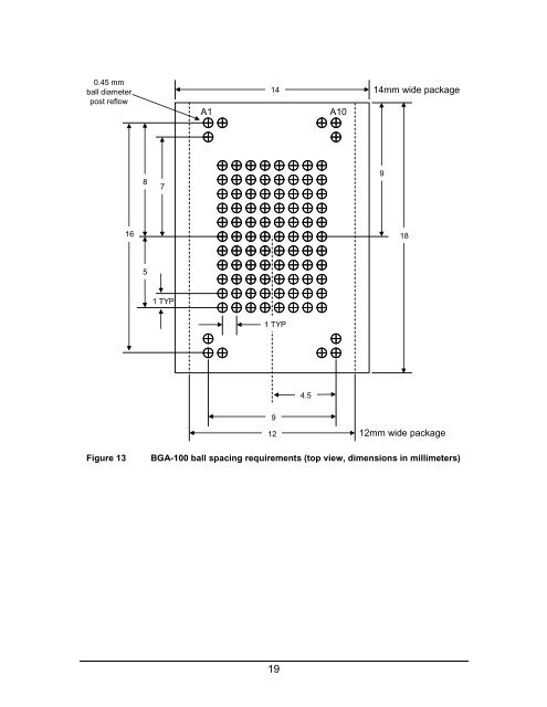
- Page 19 and 20: Note that WE_n is located at ball H
- Page 21 and 22: 0.45 mm ball diameter post reflow 0
- Page 23: A B C D E F G H J K L M N P R T U 1
- Page 27 and 28: does not implement that signal. Any
- Page 29 and 30: Signal Name M/O/R TSOP / WSOP Async
- Page 31 and 32: 2.6. CE_n Signal Requirements If on
- Page 33 and 34: 2.9. AC Overshoot/Undershoot Requir
- Page 35 and 36: Parameter Symbol Test Conditions Mi
- Page 37 and 38: capacitance may be used, or the typ
- Page 39 and 40: 2.16.2. R/B_n and SR[6] Relationshi
- Page 41 and 42: A block is the smallest erasable un
- Page 43 and 44: Multi-plane Multi-plane Lower Bit X
- Page 45 and 46: 3.2.2. Host Requirements The host s
- Page 47 and 48: 3.4. Discovery and Initialization 3
- Page 49 and 50: 4. Data Interface and Timing 4.1. D
- Page 51 and 52: CE_n ALE CLE W/R_n CLK Source Synch
- Page 53 and 54: � RE_n / W/R_n shall be set to on
- Page 55 and 56: Parameter Description tADL 3 ALE to
- Page 57 and 58: Figure 22 EZ NAND Output Reference
- Page 59 and 60: Table 23 Asynchronous Timing Modes
- Page 61 and 62: Table 24 Asynchronous Timing Modes
- Page 63 and 64: tITC 1 Interface and Timing Mode Ch
- Page 65 and 66: Description R_pulldown R_pullup Des
- Page 67 and 68: Output Impedance Maximum Minimum Un
- Page 69 and 70: The testing conditions that shall b
- Page 71 and 72: If timing mode 0 is selected, then
- Page 73 and 74: tDSS 0.2 — 0.2 — 0.2 — 0.2
- Page 75 and 76:
CLE CE_n 4.3.1.2. Address Latch Tim
- Page 77 and 78:
4.3.1.4. Data Output Cycle Timings
- Page 79 and 80:
CLE CE_n 4.3.1.6. Read Status Timin
- Page 81 and 82:
4.3.2. Source Synchronous For the c
- Page 83 and 84:
4.3.2.3. Data Input Cycle Timings D
- Page 85 and 86:
4.3.2.4. Data Input Cycle Timings,
- Page 87 and 88:
CE_n CLE ALE CLK W/R_n DQS DQ[7:0]
- Page 89 and 90:
CE_n CLE ALE CLK W/R_n DQS DQ[7:0]
- Page 91 and 92:
4.3.2.7. Satisfying Timing Requirem
- Page 93 and 94:
4.4. Command Examples 4.4.1. Asynch
- Page 95 and 96:
Figure 42 shows an example of Chang
- Page 97 and 98:
CLK CE_n CLE ALE W/R_n DQ[7:0] DQS
- Page 99 and 100:
CLK CE_n CLE ALE W/R_n DQ[7:0] DQS
- Page 101 and 102:
5. Command Definition 5.1. Command
- Page 103 and 104:
Type Opcode Vendor Specific 02h - 0
- Page 105 and 106:
CE_n CLE ALE WE_n RE_n IOx 85h Figu
- Page 107 and 108:
5.3. Reset Definition The Reset fun
- Page 109 and 110:
Cycle Type DQ[7:0] SR[6] 5.6. Read
- Page 111 and 112:
Figure 56 Read ID command using sou
- Page 113 and 114:
5.7.1. Parameter Page Data Structur
- Page 115 and 116:
Byte O/M Description 129-130 M Asyn
- Page 117 and 118:
Bit 3 when set to one indicates tha
- Page 119 and 120:
5.7.1.8. Byte 44-63: Device model T
- Page 121 and 122:
5.7.1.23. Byte 108-109: Block endur
- Page 123 and 124:
Bit 2 indicates whether the target
- Page 125 and 126:
us. As an example, if two LUNs are
- Page 127 and 128:
5.7.1.6. Byte 512-767: Redundant Pa
- Page 129 and 130:
Byte O/M Description Revision infor
- Page 131 and 132:
Bytes Value 0-15 UID 16-31 UID comp
- Page 133 and 134:
Status Register bit Composite statu
- Page 135 and 136:
Figure 62 Read Status command using
- Page 137 and 138:
program and erase operations. For E
- Page 139 and 140:
Cycle Type DQx SR[6] CMD 00h ADDR C
- Page 141 and 142:
Cycle Type DQx SR[6] As defined for
- Page 143 and 144:
Figure 67 defines the Read Cache (S
- Page 145 and 146:
Cycle Type DQx SR[6] CMD 80h ADDR C
- Page 147 and 148:
Cycle Type DQx SR[6] Cycle Type DQx
- Page 149 and 150:
C1-C2 Column address of the startin
- Page 151 and 152:
R1-R3 B Row address of the page to
- Page 153 and 154:
Cycle Type DQx SR[6] Cycle Type DQx
- Page 155 and 156:
Cycle Type DQx SR[6] Cycle Type DQx
- Page 157 and 158:
5.20. Change Read Column Definition
- Page 159 and 160:
5.22. Change Write Column Definitio
- Page 161 and 162:
5.24. Set Features Definition The S
- Page 163 and 164:
5.25. Get Features Definition The G
- Page 165 and 166:
5.26.2. I/O Drive Strength This set
- Page 167 and 168:
60h CMD D1h CMD Multi-plane Op 1 F
- Page 169 and 170:
R1B-R3B D0B-DnB Row address for pag
- Page 171 and 172:
The row addresses for all source pa
- Page 173 and 174:
6.5. Multi-plane Block Erase Figure
- Page 175 and 176:
Cycle Type DQx SR[6] B CMD 30h tWB
- Page 177 and 178:
Cycle Type DQx SR[6] Cycle Type DQx
- Page 179 and 180:
7. Behavioral Flows 7.1. Target beh
- Page 181 and 182:
7.1.3. Idle Read states T_Idle_Rd W
- Page 183 and 184:
T_CRE_RowAddrWait Wait for a row ad
- Page 185 and 186:
T_RST_LUN_AddrWait Wait for an addr
- Page 187 and 188:
T_RPP_ReadParams The target perform
- Page 189 and 190:
T_PP_LUN_Execute The target perform
- Page 191 and 192:
T_PP_RowChg_Addr Store the address
- Page 193 and 194:
7.1.10. Read command states T_RD_Ex
- Page 195 and 196:
7.1.11. Set Features command states
- Page 197 and 198:
7.1.14. Read Status Enhanced comman
- Page 199 and 200:
L_Idle_TargetRequest If Target indi
- Page 201 and 202:
7.2.4. Status states L_Status_Execu
- Page 203 and 204:
interleaving is supported. 1. Uncon
- Page 205 and 206:
L_RD_ArrayRead_Cont 1. Read of requ
- Page 207 and 208:
3. Command cycle 15h (cache program
- Page 209 and 210:
1. Unconditional � L_Idle L_PP_Ca
- Page 211 and 212:
} while(scanf("%x", &data_in) == 1)
- Page 213 and 214:
C. DEVICE SELF-INITIALIZATION WITH
- Page 215 and 216:
The following figures detail the te
- Page 217 and 218:
Cycle Type DQx R/B_n CMD 80h 212 Fi
- Page 219 and 220:
Cycle Type DQx R/B_n Cycle Type DQx
- Page 221 and 222:
Cycle Type DQ[7:0] R/B_n 216 IDLE F
- Page 223:
F. EZ NAND: END TO END DATA PATH PR