

Open NAND Flash Interface Specification - Micron
Open NAND Flash Interface Specification - Micron
Open NAND Flash Interface Specification - Micron

Create successful ePaper yourself
Turn your PDF publications into a flip-book with our unique Google optimized e-Paper software.
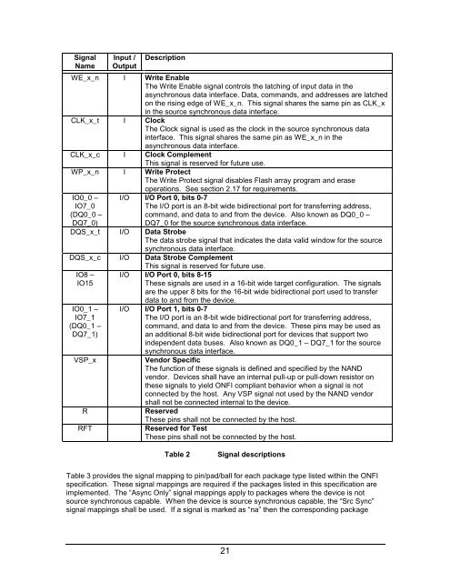
Signal<br />
Name<br />
Input /<br />
Output<br />
Description<br />
WE_x_n I Write Enable<br />
The Write Enable signal controls the latching of input data in the<br />
asynchronous data interface. Data, commands, and addresses are latched<br />
on the rising edge of WE_x_n. This signal shares the same pin as CLK_x<br />
in the source synchronous data interface.<br />
CLK_x_t I Clock<br />
The Clock signal is used as the clock in the source synchronous data<br />
interface. This signal shares the same pin as WE_x_n in the<br />
asynchronous data interface.<br />
CLK_x_c I Clock Complement<br />
WP_x_n<br />
IO0_0 –<br />
IO7_0<br />
(DQ0_0 –<br />
DQ7_0)<br />
This signal is reserved for future use.<br />
I Write Protect<br />
The Write Protect signal disables <strong>Flash</strong> array program and erase<br />
operations. See section 2.17 for requirements.<br />
I/O I/O Port 0, bits 0-7<br />
The I/O port is an 8-bit wide bidirectional port for transferring address,<br />
command, and data to and from the device. Also known as DQ0_0 –<br />
DQ7_0 for the source synchronous data interface.<br />
DQS_x_t I/O Data Strobe<br />
The data strobe signal that indicates the data valid window for the source<br />
synchronous data interface.<br />
DQS_x_c I/O Data Strobe Complement<br />
IO8 –<br />
IO15<br />
IO0_1 –<br />
IO7_1<br />
(DQ0_1 –<br />
DQ7_1)<br />
This signal is reserved for future use.<br />
I/O I/O Port 0, bits 8-15<br />
These signals are used in a 16-bit wide target configuration. The signals<br />
are the upper 8 bits for the 16-bit wide bidirectional port used to transfer<br />
data to and from the device.<br />
I/O I/O Port 1, bits 0-7<br />
The I/O port is an 8-bit wide bidirectional port for transferring address,<br />
command, and data to and from the device. These pins may be used as<br />
an additional 8-bit wide bidirectional port for devices that support two<br />
independent data buses. Also known as DQ0_1 – DQ7_1 for the source<br />
synchronous data interface.<br />
VSP_x Vendor Specific<br />
The function of these signals is defined and specified by the <strong>NAND</strong><br />
vendor. Devices shall have an internal pull-up or pull-down resistor on<br />
these signals to yield ONFI compliant behavior when a signal is not<br />
connected by the host. Any VSP signal not used by the <strong>NAND</strong> vendor<br />
shall not be connected internal to the device.<br />
R Reserved<br />
These pins shall not be connected by the host.<br />
RFT Reserved for Test<br />
These pins shall not be connected by the host.<br />
Table 2 Signal descriptions<br />
Table 3 provides the signal mapping to pin/pad/ball for each package type listed within the ONFI<br />
specification. These signal mappings are required if the packages listed in this specification are<br />
implemented. The “Async Only” signal mappings apply to packages where the device is not<br />
source synchronous capable. When the device is source synchronous capable, the “Src Sync”<br />
signal mappings shall be used. If a signal is marked as “na” then the corresponding package<br />
21


