

Open NAND Flash Interface Specification - Micron
Open NAND Flash Interface Specification - Micron
Open NAND Flash Interface Specification - Micron

Create successful ePaper yourself
Turn your PDF publications into a flip-book with our unique Google optimized e-Paper software.
output buffers. This ensures that only the LUN selected by the Read Status Enhanced command<br />
responds to a subsequent data output cycle. After a Read Status Enhanced command has been<br />
completed, the Read Status command may be used until the next multiple LUN operation is<br />
issued.<br />
When the host has issued Read Page commands to multiple LUNs at the same time, the host<br />
shall issue Read Status Enhanced before reading data from either LUN. This ensures that only<br />
the LUN selected by the Read Status Enhanced command responds to a data output cycle after<br />
being put in data output mode with a 00h command, and thus avoiding bus contention. If the host<br />
issues a Change Read Column (Enhanced) for any LUN that Read Page commands are<br />
outstanding for, then the host shall issue a Change Read Column (Enhanced) prior to transferring<br />
data from any subsequent LUN that is part of the multiple LUN read sequence. An example<br />
sequence is shown below:<br />
1) Read Page command issued to LUN 0<br />
2) Read Page command issued to LUN 1<br />
3) Read Status Enhanced selects LUN 0<br />
4) Change Read Column (Enhanced) issued to LUN 0 (if needed by host)<br />
5) Data transferred from LUN 0<br />
6) Read Status Enhanced selects LUN 1<br />
7) Change Read Column (Enhanced) issued to LUN 1 (required if action 4 taken)<br />
8) Data transferred from LUN 1<br />
The host may substitute Change Read Column Enhanced for the Read Status Enhanced /<br />
Change Read Column sequence if all LUNs are not busy.<br />
3.2. Factory Defect Mapping<br />
The <strong>Flash</strong> array is not presumed to be pristine, and a number of defects may be present that<br />
renders some blocks unusable. Block granularity is used for mapping factory defects since those<br />
defects may compromise the block erase capability.<br />
3.2.1. Device Requirements<br />
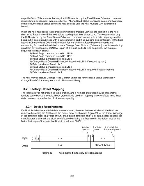
If a block is defective and 8-bit data access is used, the manufacturer shall mark the block as<br />
defective by setting the first byte in the defect area, as shown in Figure 20, of the first or last page<br />
of the defective block to a value of 00h. If a block is defective and 16-bit data access is used, the<br />
manufacturer shall mark the block as defective by setting the first word in the defect area of the<br />
first or last page of the defective block to a value of 0000h.<br />
Byte<br />
Area<br />
0 1 2<br />
…<br />
n/a<br />
Figure 20 Area marked in factory defect mapping<br />
39<br />
# of data<br />
bytes - 1<br />
# of data<br />
bytes<br />
…<br />
Defect Area<br />
# of data bytes +<br />
# of spare bytes - 1


