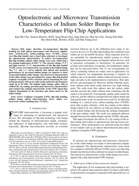
Optoelectronic and microwave transmission characteristics of indium ...
Optoelectronic and microwave transmission characteristics of indium ...
Optoelectronic and microwave transmission characteristics of indium ...

You also want an ePaper? Increase the reach of your titles
YUMPU automatically turns print PDFs into web optimized ePapers that Google loves.
IEEE TRANSACTIONS ON ADVANCED PACKAGING, VOL. 29, NO. 3, AUGUST 2006 409<br />
<strong>Optoelectronic</strong> <strong>and</strong> Microwave Transmission<br />
Characteristics <strong>of</strong> Indium Solder Bumps for<br />
Low-Temperature Flip-Chip Applications<br />
Kun-Mo Chu, Student Member, IEEE, Jung-Hwan Choi, Jung-Sub Lee, Han Seo Cho, Seong-Ook Park,<br />
Hyo-Hoon Park, Member, IEEE, <strong>and</strong> Duk Young Jeon<br />
Abstract—This paper describes low-temperature flip-chip<br />
bonding for both optical interconnect <strong>and</strong> <strong>microwave</strong> applications.<br />
Vertical-cavity surface-emitting laser (VCSEL) arrays<br />
were flip-chip bonded onto a fused silica substrate to investigate<br />
the optoelectronic <strong>characteristics</strong>. To achieve low-temperature<br />
flip-chip bonding, <strong>indium</strong> solder bumps were used, which had a<br />
low melting temperature <strong>of</strong> 156.7 C. The current–voltage ( – )<br />
<strong>and</strong> light–current ( – ) <strong>characteristics</strong> <strong>of</strong> the flip-chip bonded<br />
VCSEL arrays were improved by Ag coating on the <strong>indium</strong> bump.<br />
The – <strong>and</strong> – curves indicate that optical <strong>and</strong> electrical<br />
performances <strong>of</strong> Ag-coated <strong>indium</strong> bumps are superior to those<br />
<strong>of</strong> uncoated <strong>indium</strong> solder bumps. The <strong>microwave</strong> <strong>characteristics</strong><br />
<strong>of</strong> the solder bumps were investigated by using a flip-chip-bonded<br />
coplanar waveguide (CPW) structure <strong>and</strong> by measuring the scattering<br />
parameter with an on-wafer probe station for the frequency<br />
range up to 40 GHz. The <strong>indium</strong> solder bumps, either with or<br />
without the Ag coating, provided good <strong>microwave</strong> <strong>characteristics</strong><br />
<strong>and</strong> retained the original characteristic <strong>of</strong> the CPW signal lines<br />
without degradation <strong>of</strong> the insertion <strong>and</strong> return losses by the<br />
solder bumps.<br />
Index Terms—Coplanar waveguide (CPW), flip-chip bonding,<br />
<strong>indium</strong> bump, optical interconnection, silver, solder, vertical-cavity<br />
surface-emitting laser (VCSEL).<br />
I. INTRODUCTION<br />
FLIP-CHIP interconnection is becoming a popular technique<br />
for packaging <strong>of</strong> optoelectronic <strong>and</strong> <strong>microwave</strong><br />
devices. The advantages <strong>of</strong> flip-chip technology with bumps<br />
include the reduction <strong>of</strong> interconnection length, resistance,<br />
<strong>and</strong> inductance in high-frequency <strong>and</strong> wide-b<strong>and</strong> systems.<br />
Especially, flip-chip interconnection provides an excellent<br />
Manuscript received February 1, 2005; revised June 8, 2005. This work was<br />
supported in part by the Center for Electronic Packaging Materials (ERC) <strong>of</strong><br />
MOST/KOSEF under Grant R11-2000-085-10001-0 <strong>and</strong> in part by the Korea<br />
Ministry <strong>of</strong> Science <strong>and</strong> Technology (MOST) under the national program for<br />
tera-level nanodevices as one <strong>of</strong> the “21st century frontier R&D projects.”<br />
K.-M. Chu, <strong>and</strong> J.-S. Lee are with the Department <strong>of</strong> Materials Science <strong>and</strong><br />
Engineering, Korea Advanced Institute <strong>of</strong> Science <strong>and</strong> Technology, Daejeon<br />
305-701, Korea, <strong>and</strong> also with the Optical Interconnection <strong>and</strong> Switching Laboratory,<br />
Information <strong>and</strong> Communications University, Daejeon 305–714, Korea.<br />
J.-H. Choi <strong>and</strong> S.-O. Park are with the Microwave <strong>and</strong> Antenna Laboratory,<br />
Information <strong>and</strong> Communications University, Daejeon 305-714, Korea.<br />
H. S. Cho is with the Optical Interconnection <strong>and</strong> Switching Laboratory,<br />
Information <strong>and</strong> Communications University, Daejeon 305-714, Korea. He<br />
is also with the Samsung Electro-Mechanics Corporation, Ltd., Yeongi-Gun<br />
Chungnam 339-702, Korea.<br />
H.-H. Park is with the Optical Interconnection <strong>and</strong> Switching Laboratory, Information<br />
<strong>and</strong> Communications University, Daejeon 305-714, Korea.<br />
D. Y. Jeon is with the Department <strong>of</strong> Materials Science <strong>and</strong> Engineering,<br />
Korea Advanced Institute <strong>of</strong> Science <strong>and</strong> Technology, Daejeon 305-701, Korea.<br />
Digital Object Identifier 10.1109/TADVP.2006.875417<br />
electrical behavior up to the millimeter-wave range in <strong>microwave</strong><br />
devices [1]. For flip-chip bonding, the commonly used<br />
solders are Au–Sn <strong>and</strong> Pb–Sn alloys. These materials, however,<br />
are unsuitable for optoelectronic hybrid systems in which<br />
high-temperature processing can degrade optical devices, such<br />
as polymeric waveguides or microlenses. In particular, for<br />
acrylate series polymeric waveguides, low-temperature solders<br />
that can be processed below 160 C are recommended [2].<br />
Alloys containing <strong>indium</strong> are widely used in applications for<br />
which relatively low temperature processing is required. In<br />
addition, due to its ductility, <strong>indium</strong> solder has become increasingly<br />
prevalent in the implementation <strong>of</strong> photonics, fiber-optic<br />
devices, <strong>and</strong> packaging [3]. However, during soldering operations,<br />
<strong>indium</strong> easily forms oxides that have very high melting<br />
point. The solid oxide film adheres onto the molten solder<br />
<strong>and</strong> thus prevents the solder solution from contacting with the<br />
surface to be joined [4]. Consequently, quality joints cannot be<br />
achieved, <strong>and</strong> the adhesion strength between <strong>indium</strong> bump <strong>and</strong><br />
chip pad becomes weak. In our previous work [5], for flip-chip<br />
bonding <strong>of</strong> a vertical-cavity surface-emitting laser (VCSEL)<br />
array chip on glass substrate, a thin Ag coating on the <strong>indium</strong><br />
bumps found to be very effective at both preventing oxidation<br />
<strong>of</strong> the <strong>indium</strong> bumps <strong>and</strong> decreasing the melting temperature<br />
<strong>of</strong> the pure <strong>indium</strong> solder. The result was enhanced adhesion<br />
strength between the <strong>indium</strong> bumps <strong>and</strong> the VCSEL chip pads.<br />
This paper investigates the effects <strong>of</strong> a Ag coating on the <strong>indium</strong><br />
bump with respect to optoelectronic <strong>and</strong> <strong>microwave</strong> performances.<br />
These performances are analyzed using two kinds<br />
<strong>of</strong> test samples such as an optical interconnection plate <strong>and</strong> a<br />
coplanar waveguide (CPW) package.<br />
II. EXPERIMENT<br />
To measure the optoelectronic <strong>and</strong> <strong>microwave</strong> <strong>characteristics</strong><br />
<strong>of</strong> the solder bumps, two kinds <strong>of</strong> interconnection samples<br />
were prepared. The optoelectronic <strong>characteristics</strong> were tested<br />
for a sample in which the 850-nm VCSEL arrays were flip-chip<br />
bonded onto the fused silica substrate by means <strong>of</strong> solder bumps.<br />
The <strong>microwave</strong> <strong>characteristics</strong> <strong>of</strong> the solder bumps were investigated<br />
with a flip-chip-bonded CPW structure.<br />
A. Fabrication <strong>of</strong> Optical Interconnection Samples<br />
The application <strong>of</strong> low-temperature flip-chip bonding is targeted<br />
to the optical interconnection plate [2] where a thermally<br />
weak polymeric waveguide is integrated with optical devices, as<br />
1521-3323/$20.00 © 2006 IEEE
410 IEEE TRANSACTIONS ON ADVANCED PACKAGING, VOL. 29, NO. 3, AUGUST 2006<br />
Fig. 1.<br />
Architecture <strong>of</strong> the optical interconnection plate assembled with a conventional PCB. (Color version available online at http://ieeexplore.ieee.org.)<br />
Fig. 3. Flip-chip configuration in CPW test. (A 0 A : cross section <strong>of</strong><br />
flip-chip assembled CPW package). (Color version available online at<br />
http://ieeexplore.ieee.org.)<br />
Fig. 2. Images <strong>of</strong> (a) as-deposited solder bumps before reflow <strong>and</strong> (b) the<br />
flip-chip bonded VCSEL array on the quartz substrate. (Color version available<br />
online at http://ieeexplore.ieee.org.)<br />
shown in Fig. 1. The VCSEL <strong>and</strong> photo detector (PD) chips are<br />
flip-chip bonded onto the top surface <strong>of</strong> a transparent substrate,<br />
<strong>and</strong> a polymeric waveguide is formed on the bottom surface <strong>of</strong><br />
the substrate. In the fabrication <strong>of</strong> this interconnection plate, the<br />
waveguide is formed first <strong>and</strong> then the VCSEL/PD chips are<br />
bonded. If these processes were reversed, the spin-coating <strong>of</strong><br />
the waveguide materials would be difficult [2]. Thus, to protect<br />
the polymeric waveguide from thermal damage during flip-chip<br />
bonding, a low melting temperature bump material is needed.<br />
In the test sample for the bump metal, metal layers <strong>of</strong> both<br />
Ag-coated <strong>indium</strong> <strong>and</strong> uncoated <strong>indium</strong> were deposited for<br />
comparison. The dimensions <strong>of</strong> the bumps were 6 m in height<br />
<strong>and</strong> 80 m in diameter. The metal lines <strong>and</strong> bumps are shown<br />
in Fig. 2(a). When the VCSEL array chip was flip-chip bonded<br />
onto the substrate, the bonding temperatures was 150 C <strong>and</strong><br />
the bonding pressure was 500 gf. The two-channel VCSEL<br />
array is 500 470 m, with a thickness <strong>of</strong> 200 m. The<br />
flip-chip-bonded VCSEL array chip is shown in Fig. 2(b).<br />
B. Fabrication <strong>of</strong> CPW Flip-Chip Interconnection Samples<br />
The test sample to measure the <strong>microwave</strong> <strong>characteristics</strong> was<br />
composed <strong>of</strong> CPWs on a quartz substrate <strong>and</strong> a quartz chip,<br />
as shown in Fig. 3. The chip was flip-chip bonded onto the<br />
substrate using the bumps formed on the substrate, as shown<br />
in Fig. 4(a). The flip-chip-bonded CPW sample is shown in<br />
Fig. 4(b). The test chip with the dimensions <strong>of</strong> 1 1 0.7 mm<br />
has 50- CPW through lines. The substrate has the same 50-
CHU et al.: OPTOELECTRONIC AND MICROWAVE TRANSMISSION CHARACTERISTICS 411<br />
Fig. 5.<br />
EDS elemental distribution mapping <strong>of</strong> diffused Ag in <strong>indium</strong> solder.<br />
Fig. 4. Images <strong>of</strong> (a) as-deposited solder bumps before reflow <strong>and</strong> (b)<br />
the flip-chip bonded CPW structure. (Color version available online at<br />
http://ieeexplore.ieee.org.)<br />
TABLE I<br />
DESIGN TABLE FOR THE CPW TEST SYSTEMS<br />
Fig. 6. Experimental setup to measure the light output power <strong>of</strong><br />
flip-chip-assembled VCSEL array. (Color version available online at<br />
http://ieeexplore.ieee.org.)<br />
were deposited via e-beam evaporation. The Ti/Ni/Au layers<br />
were used for the under bump metallurgy (UBM). The solder<br />
bumps were formed only on the substrate by means <strong>of</strong> thermal<br />
evaporation <strong>and</strong> lift-<strong>of</strong>f processes. The thickness <strong>of</strong> the Ag<br />
layer coated on the <strong>indium</strong> was about 2000 . After deposition<br />
<strong>of</strong> solder bump, reflow processing was applied at a temperature<br />
above the melting point <strong>of</strong> <strong>indium</strong>. The chips were aligned <strong>and</strong><br />
bonded using a flip-chip bonder (Toray, FC1500 series). During<br />
the alignment process, a two-sight camera unit was inserted between<br />
the chip <strong>and</strong> the substrate. After the alignment operation,<br />
the bonding head was lowered, <strong>and</strong> the bonding operation was<br />
performed under a specific contact pressure <strong>of</strong> 500 gf [6].<br />
CPW lines as the test chip. Detailed dimensions <strong>and</strong> deduced<br />
parameters for the 50- CPW structure are listed in Table I.<br />
C. Solder Bump Formation <strong>and</strong> Flip-Chip Process<br />
The two solder bump materials, for a comparison <strong>of</strong> the<br />
Ag-coated <strong>indium</strong> <strong>and</strong> the uncoated <strong>indium</strong>, were formed in<br />
both optical <strong>and</strong> CPW interconnection samples. In the metal<br />
lines, three layers <strong>of</strong> metal, Ti (100 )/Ni (400 )/Au (3000 )<br />
III. RESULTS AND DISCUSSION<br />
A. Interface <strong>of</strong> Ag-Coated Indium Solder<br />
In our previous research [7], it was found that a fracture<br />
occurred between <strong>indium</strong> solder bump <strong>and</strong> the chip pad during<br />
a die shear test. The problem occurred because the bonding<br />
temperature was lower than the melting point <strong>of</strong> <strong>indium</strong>. The<br />
fracture is attributed to the formation <strong>of</strong> <strong>indium</strong> oxide, which<br />
prevents good adhesion between the <strong>indium</strong> bump <strong>and</strong> the<br />
VCSEL chip pad. However, a Ag layer coated onto the <strong>indium</strong><br />
solder bump effectively enhances the adhesion strength<br />
between the <strong>indium</strong> bump <strong>and</strong> the VCSEL chip pads by decreasing<br />
the melting temperature <strong>of</strong> the <strong>indium</strong> solder <strong>and</strong><br />
protecting it from oxidation [5]. In this paper, the alloying state
412 IEEE TRANSACTIONS ON ADVANCED PACKAGING, VOL. 29, NO. 3, AUGUST 2006<br />
Fig. 7. <strong>Optoelectronic</strong> <strong>characteristics</strong> <strong>of</strong> flip-chip-bonded VCSEL arrays<br />
(a) I–V curves <strong>and</strong> (b) L–I curves. (Color version available online at<br />
http://ieeexplore.ieee.org.)<br />
<strong>of</strong> the Ag/In interface is analyzed. Fig. 5 shows the energy<br />
dispersive spectroscopy (EDS) elemental distribution mapping<br />
<strong>of</strong> diffused Ag in an <strong>indium</strong> solder. It can be inferred that the<br />
Ag atoms are deeply diffused into the <strong>indium</strong> solder, despite<br />
the small amount <strong>of</strong> Ag involved. In general, the Ag diffuses<br />
rapidly into <strong>indium</strong> via an interstitial mechanism, <strong>and</strong> <strong>indium</strong><br />
diffuses into silver through grain boundaries with a diffusion<br />
coefficient <strong>of</strong> 2.4 10 m s <strong>and</strong> an activation energy<br />
<strong>of</strong> 0.42 eV [8]. Therefore, immediately after deposition, the<br />
Ag layer interacts with the <strong>indium</strong> to form a AgIn compound<br />
layer due to the high interdiffusion coefficient [9]. Formation<br />
<strong>of</strong> a AgIn compound was identified from scanning electron<br />
microscopy (SEM) <strong>and</strong> EDS analyses.<br />
B. <strong>Optoelectronic</strong> Characteristics <strong>of</strong> Flip-Chip-Bonded<br />
VCSEL Array<br />
Fig. 6 shows the experimental setup used to measure the light<br />
output power <strong>of</strong> the flip-chip assembled VCSEL array. The <strong>characteristics</strong><br />
<strong>of</strong> the VCSEL arrays that were flip-chip bonded using<br />
Fig. 8. Measured (a) insertion loss (S ) <strong>and</strong> (b) return loss (S ) for <strong>indium</strong><br />
bump <strong>and</strong> Ag-coated <strong>indium</strong> bump (total CPW line length: 4 mm). (Color<br />
version available online at http://ieeexplore.ieee.org.)<br />
either a Ag-coated <strong>indium</strong> bump or an uncoated <strong>indium</strong> bump<br />
are compared by means <strong>of</strong> – <strong>and</strong> – inspections. In this<br />
paper, two-channel VCSEL arrays operating at 850-nm wavelength<br />
range with rates <strong>of</strong> 2.5 Gb/s were used. Fig. 7(a) shows<br />
the – curves <strong>of</strong> the flip-chip-bonded VCSEL. It inferred that<br />
the resistance <strong>of</strong> a Ag-coated <strong>indium</strong> bump is slightly lower<br />
than that <strong>of</strong> the uncoated <strong>indium</strong> bump. The – <strong>characteristics</strong><br />
<strong>of</strong> the VCSELs were compared in Fig. 7(b). The light output<br />
power <strong>of</strong> the Ag-coated <strong>indium</strong> bump is higher than that <strong>of</strong> the<br />
<strong>indium</strong> bump. In addition, the Ag coating on the <strong>indium</strong> bumps<br />
decreases the threshold current <strong>of</strong> the VCSEL from 50 to 43 mA.<br />
Therefore, the – <strong>and</strong> – curves indicate that the Ag-coated<br />
<strong>indium</strong> bumps are superior to the uncoated <strong>indium</strong> solder bumps<br />
with regard to optical <strong>and</strong> electrical performances.<br />
C. Characterization <strong>of</strong> a Flip-Chip Interconnect at<br />
Frequencies Up to 40 GHz<br />
The RF <strong>and</strong> <strong>microwave</strong> <strong>characteristics</strong> <strong>of</strong> the flip-chipbonded<br />
CPW samples were analyzed for the entire frequency
CHU et al.: OPTOELECTRONIC AND MICROWAVE TRANSMISSION CHARACTERISTICS 413<br />
Fig. 10. Joint cross-sectional SEM images <strong>of</strong> CPW package using (a) <strong>indium</strong><br />
<strong>and</strong> (b) Ag-coated <strong>indium</strong> bumps.<br />
Fig. 9. Measured (a) insertion loss (S ) <strong>and</strong> (b) return loss (S ) for <strong>indium</strong><br />
bump <strong>and</strong> Ag-coated <strong>indium</strong> bump (total CPW line length: 10 mm). (Color<br />
version available online at http://ieeexplore.ieee.org.)<br />
range from 0.1 to 40 GHz. It has been reported that the RF<br />
performance <strong>of</strong> the flip-chip bonded structure is influenced by<br />
different bump materials [10], [11]. In this paper, the effect <strong>of</strong><br />
the Ag coating on the <strong>indium</strong> bumps on the RF performances<br />
was investigated.<br />
The measurement <strong>of</strong> the scattering parameters was performed<br />
using an Agilent 8722ES network analyzer with an on-wafer<br />
probe station for the frequency range up to 40 GHz. Figs. 8 <strong>and</strong><br />
9 show the measured reflection <strong>and</strong> insertion losses, in terms <strong>of</strong><br />
frequency, corresponding to total CPW lengths <strong>of</strong> 4 <strong>and</strong> 10 mm,<br />
respectively. In both cases, when the total CPW line length is<br />
10 mm, the insertion loss is about 3.3 dB/cm at 20 GHz <strong>and</strong> the<br />
return loss is less than 13 dB, as shown in Fig. 9. The <strong>microwave</strong><br />
<strong>transmission</strong> effect <strong>of</strong> the Ag coating is negligible by comparison<br />
with uncoated <strong>indium</strong> bumps. The measured results for the<br />
CPW only are an insertion loss <strong>of</strong> about 3.3 dB/cm at 20 GHz<br />
<strong>and</strong> a reflection loss <strong>of</strong> less than 14 dB. Thus, both Ag-coated<br />
<strong>and</strong> uncoated <strong>indium</strong> solder bumps can be used in flip-chip interconnects,<br />
while preserving the original <strong>characteristics</strong> <strong>of</strong> CPW<br />
signal lines.<br />
D. Cross Sections <strong>of</strong> Flip-Chip Assembled CPW Samples<br />
SEM <strong>and</strong> EDS analyses were performed on the joint cross<br />
sections <strong>of</strong> the CPW packages. Fig. 10(a) <strong>and</strong> (b), shows the<br />
joint cross-sectional SEM images <strong>of</strong> the CPW package using<br />
<strong>indium</strong> <strong>and</strong> Ag-coated <strong>indium</strong> bumps, respectively. The SEM<br />
<strong>and</strong> EDS results indicate that the joint [Fig. 10(a)] consists <strong>of</strong><br />
an <strong>indium</strong>–gold alloy with embedded intermetallic grains <strong>of</strong><br />
AuIn . In addition, SEM <strong>and</strong> EDS results indicate that the joint<br />
[Fig. 10(b)] consists <strong>of</strong> an In–Au–Ag mixture alloy with embedded<br />
intermetallic grains [5]. The joint microstructure <strong>of</strong> the<br />
Ag-coated <strong>indium</strong> solder is similar to that <strong>of</strong> <strong>indium</strong> solder. The<br />
height <strong>of</strong> the solder bump was changed from 6.0 to 3.6 m after<br />
the flip-chip bonding process.<br />
IV. CONCLUSION<br />
This paper presents low-temperature flip-chip bonding for<br />
both optical interconnect <strong>and</strong> <strong>microwave</strong> applications, comparing<br />
the use <strong>of</strong> a Ag-coated <strong>indium</strong> bump <strong>and</strong> an uncoated<br />
<strong>indium</strong> bump. Coating a thin Ag layer onto the <strong>indium</strong> surface<br />
enhanced the optoelectronic <strong>characteristics</strong> <strong>of</strong> an <strong>indium</strong><br />
bump. However, the effects <strong>of</strong> the Ag coating on <strong>microwave</strong><br />
<strong>characteristics</strong> are negligible. Both the Ag-coated <strong>and</strong> uncoated<br />
<strong>indium</strong> solder bumps maintain the original <strong>characteristics</strong> <strong>of</strong><br />
CPW signal lines almost without additional losses from the<br />
flip-chip-bonded bumps.
414 IEEE TRANSACTIONS ON ADVANCED PACKAGING, VOL. 29, NO. 3, AUGUST 2006<br />
REFERENCES<br />
[1] A. Koschel <strong>and</strong> S. Cyrusian, “Comprehensive characterization <strong>of</strong> flip<br />
chip contacting methods for <strong>microwave</strong> <strong>and</strong> optoelectronic applications,”<br />
in Proc. SBMO/IEEE MTT-S IMOC, 1995, pp. 340–345.<br />
[2] H. S. Cho, K.-M. Chu, S. K. Kang, B. S. Rho, W. H. Kim, J.-S. Kim,<br />
J.-J. Kim, <strong>and</strong> H.-H. Park, “Compact packaging <strong>of</strong> optical <strong>and</strong> electronic<br />
components for on board optical interconnects,” IEEE Trans. Adv.<br />
Packag., vol. 28, no. 1, pp. 114–120, Feb. 2005.<br />
[3] S. Choe, W. W. So, <strong>and</strong> C. C. Lee, “Low temperature fluxless bonding<br />
technique using In-Sn composite,” Proc. Electron. Compon. Technol.<br />
Conf., pp. 114–118, 2000.<br />
[4] Y. C. Chen, W. W. So, <strong>and</strong> C. C. Lee, “A fluxless bonding technology<br />
using <strong>indium</strong>–silver multiplayer composites,” IEEE Trans. Compon.,<br />
Packag., Manuf. Technol. A, vol. CPMT-20, no. 1, pp. 46–51, Mar. 1977.<br />
[5] K.-M. Chu, J.-S. Lee, H. S. Cho, H. H. Park, <strong>and</strong> D. Y. Jeon, “A fluxless<br />
flip chip bonding for VCSEL arrays using silver-coated <strong>indium</strong><br />
solder bumps,” IEEE Trans. Electron. Packag. Manuf., vol. 27, no. 4,<br />
pp. 246–253, Oct. 2004.<br />
[6] T. Suga, T. Itoh, Z. Xu, M. Tomita, <strong>and</strong> A. Yamauchi, “Surface-activated<br />
bonding for new flip chip <strong>and</strong> bumpless interconnect systems,” in Proc.<br />
Electron. Compon. Technol. Conf., 2002, pp. 105–111.<br />
[7] K.-M. Chu, J.-S. Lee, H. S. Cho, B. S. Rho, H.-H. Park, <strong>and</strong> D. Y.<br />
Jeon, “Characteristics <strong>of</strong> <strong>indium</strong> bump for flip-chip bonding used in<br />
polymeric-waveguide-integrated optical interconnection systems,” Jpn.<br />
J. Appl. Phys., vol. 43, no. 8B, pp. 5922–5927, 2004.<br />
[8] V. Simic <strong>and</strong> Z. Marinkovic, “Room temperature interactions in Ag<br />
metals thin film couples,” Thin Solid Films, vol. 61, pp. 149–160, 1979.<br />
[9] R. Roy <strong>and</strong> S. K. Sen, “The kinetics <strong>of</strong> formation <strong>of</strong> intermetallics in<br />
Ag/In thin film couples,” Thin Solid Films, vol. 197, pp. 303–318, 1992.<br />
[10] J. Heyen, J. Schroeder, <strong>and</strong> A. F. Jacob, “Low-cost flip-chip alternatives<br />
for millimeter wave applications,” in IEEE MTT-S Dig., 2002, pp.<br />
2205–2208.<br />
[11] J. M. Vahter, J. J. Heikkinen, J. J. Tanskanen, A. K. Seppala, <strong>and</strong> E. O.<br />
Ristolainen, “Rf-performance <strong>of</strong> a low-cost flip chip assembly,” in Proc.<br />
IPACK, 2001. 15609.<br />
Kun-Mo Chu (S’06) received the B.S. degree<br />
in materials science <strong>and</strong> engineering from Korea<br />
University, Seoul, in 2001 <strong>and</strong> the M.S. degree in<br />
materials science <strong>and</strong> engineering from the Korea<br />
Advanced Institute <strong>of</strong> Science <strong>and</strong> Technology<br />
(KAIST), Daejeon, in 2003, where he is currently<br />
pursuing the Ph.D. degree.<br />
He is also a Research Assistant with the Optical<br />
Interconnection <strong>and</strong> Switching Laboratory, Information<br />
<strong>and</strong> Communications University, Daejeon. His<br />
research interests include optical interconnection architecture<br />
<strong>and</strong> flip-chip technology for electronic <strong>and</strong> photonic devices.<br />
Jung-Hwan Choi received the B.S. degree in<br />
computer engineering <strong>and</strong> electrical engineering<br />
from H<strong>and</strong>ong University, Pohang, Korea, in 2002<br />
<strong>and</strong> the M.S. degree in electrcal engineering from<br />
the Information <strong>and</strong> Communications University,<br />
Daejeon, Korea, in 2005, where he is currently<br />
pursuing the Ph.D. degree.<br />
His research interests include millimeter/<strong>microwave</strong><br />
measurement systems.<br />
Jung-Sub Lee received the B.S. degree in materials<br />
science <strong>and</strong> engineering from the Korea Advanced<br />
Institute <strong>of</strong> Science <strong>and</strong> Technology (KAIST),<br />
Daejeon, in 2002, where he is currently pursuing the<br />
Ph.D. degree.<br />
He is also a Research Assistant with the Optical<br />
Interconnection <strong>and</strong> Switching Laboratory, Information<br />
<strong>and</strong> Communications University, Daejeon. His<br />
research interests include flip-chip technology <strong>and</strong><br />
solder bumping processes in SIP systems.<br />
Han Seo Cho received the Ph.D. degree in materials<br />
science <strong>and</strong> engineering from the Korea Advanced<br />
Institute <strong>of</strong> Science <strong>and</strong> Technology (KAIST), Daejeon,<br />
in 1999.<br />
He worked as a Postdoctoral Researcher with The<br />
Johns Hopkins University, Baltimore, MD, until<br />
2001. He is currently a Research Pr<strong>of</strong>essor in the<br />
Information <strong>and</strong> Communications University (ICU),<br />
Daejeon, , <strong>and</strong> his research interests include optical<br />
material characterization, design <strong>and</strong> demonstration<br />
<strong>of</strong> chip-to-chip optical interconnection using<br />
electrooptical printed circuit boards (EOCBs). He is also with the Samsung<br />
Electro-Mechanics Corporation, Ltd., Chungnam, Korea.<br />
Seong-Ook Park received the Ph.D. degree in<br />
electrical engineering from Arizona State University<br />
(ASU), Tempe, in 1997.<br />
From March 1989 to August 1993, he was a<br />
Research Engineer with Korea Telecom, Daejeon,<br />
working with <strong>microwave</strong> systems <strong>and</strong> networks. He<br />
later joined the Telecommunication Research Center,<br />
ASU, until his departure in September 1997. Since<br />
October 1997, he has been with the Information <strong>and</strong><br />
Communications University, Daejeon, as an Associate<br />
Pr<strong>of</strong>essor. His research interests include 4G<br />
h<strong>and</strong>set antennas, millimeter/<strong>microwave</strong> systems, <strong>and</strong> analytical <strong>and</strong> numerical<br />
techniques in the area <strong>of</strong> electromagnetics.<br />
Dr. Park is a member <strong>of</strong> the Phi Kappa Phi.<br />
Hyo-Hoon Park (M’94) received the Ph.D. degree<br />
in material science <strong>and</strong> engineering from the Korea<br />
Advanced Institute <strong>of</strong> Science <strong>and</strong> Technology<br />
(KAIST), Daejeon, in 1985.<br />
From 1985 to 1986, he worked in the area <strong>of</strong> compound<br />
semiconductor devices at Stanford University,<br />
Stanford, CA, as a Postdoctoral Scholar. From 1986<br />
to 1997, he worked at the Electronics <strong>and</strong> Telecommunications<br />
Research Institute in area <strong>of</strong> high-speed<br />
electronic devices <strong>and</strong> vertical-cavity surface-emitting<br />
lasers. Since 1998, he has been a Pr<strong>of</strong>essor in<br />
the Optical Communication Group, Optical Interconnection <strong>and</strong> Switching Laboratory,<br />
Information <strong>and</strong> Communications University (ICU), Daejeon. Since<br />
joining ICU, he has been studying optical interconnection for chip-to-chip <strong>and</strong><br />
board-to-board data links, optical transceiver modules, <strong>and</strong> optical switching<br />
components for optical communication systems <strong>and</strong> networks.<br />
Duk Young Jeon received the B.S. degree from<br />
Seoul National University, Seoul, Korea, in 1976,<br />
the M.S. degree in applied physics from the Korea<br />
Advanced Institute <strong>of</strong> Science <strong>and</strong> Technology<br />
(KAIST), Daejeon, in 1979, <strong>and</strong> the Ph.D. degree in<br />
physics from Lehigh University, Bethlehem, PA, in<br />
1988.<br />
In 1988, he joined AT&T Bell Laboratories, Allentown,<br />
PA, as a Member <strong>of</strong> Technical Staff, where<br />
he was involved in the development <strong>of</strong> advanced<br />
lithography for submicron CMOS technology. Later,<br />
he was involved in researching gate technology for 0.1-m CMOS, <strong>and</strong><br />
plasma processing <strong>and</strong> device study for the high-speed BiCMOS technology at<br />
AT&T, Holmdel, NJ, <strong>and</strong> backend integration for deep submicrometer modular<br />
BiCMOS technology at AT&T, Murray Hill, NJ. Since 1994, he has been with<br />
KAIST, as a Pr<strong>of</strong>essor <strong>of</strong> Materials Science <strong>and</strong> Engineering. His research<br />
interests are in display materials <strong>and</strong> devices, such as phosphors, carbon<br />
nanotubes, optical packaging, <strong>and</strong> optical MEMs devices.