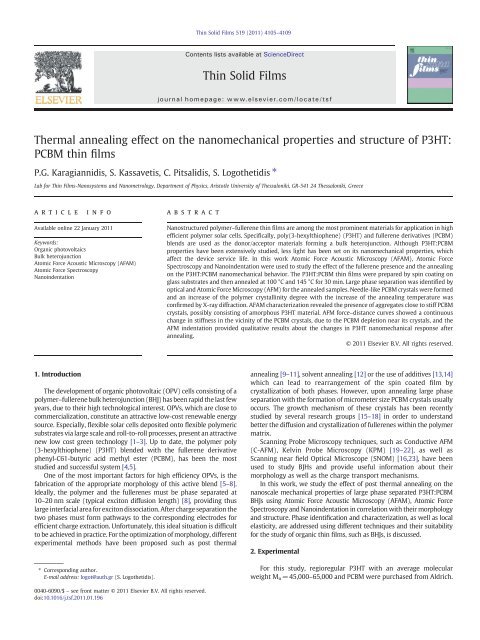
Thermal annealing effect on the nanomechanical properties and ...
Thermal annealing effect on the nanomechanical properties and ...
Thermal annealing effect on the nanomechanical properties and ...

You also want an ePaper? Increase the reach of your titles
YUMPU automatically turns print PDFs into web optimized ePapers that Google loves.
Thin Solid Films 519 (2011) 4105–4109<br />
C<strong>on</strong>tents lists available at ScienceDirect<br />
Thin Solid Films<br />
journal homepage: www.elsevier.com/locate/tsf<br />
<str<strong>on</strong>g>Thermal</str<strong>on</strong>g> <str<strong>on</strong>g>annealing</str<strong>on</strong>g> <str<strong>on</strong>g>effect</str<strong>on</strong>g> <strong>on</strong> <strong>the</strong> <strong>nanomechanical</strong> <strong>properties</strong> <strong>and</strong> structure of P3HT:<br />
PCBM thin films<br />
P.G. Karagiannidis, S. Kassavetis, C. Pitsalidis, S. Logo<strong>the</strong>tidis ⁎<br />
Lab for Thin Films-Nanosystems <strong>and</strong> Nanometrology, Department of Physics, Aristotle University of Thessal<strong>on</strong>iki, GR-541 24 Thessal<strong>on</strong>iki, Greece<br />
article<br />
info<br />
abstract<br />
Available <strong>on</strong>line 22 January 2011<br />
Keywords:<br />
Organic photovoltaics<br />
Bulk heterojuncti<strong>on</strong><br />
Atomic Force Acoustic Microscopy (AFAM)<br />
Atomic Force Spectroscopy<br />
Nanoindentati<strong>on</strong><br />
Nanostructured polymer–fullerene thin films are am<strong>on</strong>g <strong>the</strong> most prominent materials for applicati<strong>on</strong> in high<br />
efficient polymer solar cells. Specifically, poly(3-hexylthiophene) (P3HT) <strong>and</strong> fullerene derivatives (PCBM)<br />
blends are used as <strong>the</strong> d<strong>on</strong>or/acceptor materials forming a bulk heterojuncti<strong>on</strong>. Although P3HT:PCBM<br />
<strong>properties</strong> have been extensively studied, less light has been set <strong>on</strong> its <strong>nanomechanical</strong> <strong>properties</strong>, which<br />
affect <strong>the</strong> device service life. In this work Atomic Force Acoustic Microscopy (AFAM), Atomic Force<br />
Spectroscopy <strong>and</strong> Nanoindentati<strong>on</strong> were used to study <strong>the</strong> <str<strong>on</strong>g>effect</str<strong>on</strong>g> of <strong>the</strong> fullerene presence <strong>and</strong> <strong>the</strong> <str<strong>on</strong>g>annealing</str<strong>on</strong>g><br />
<strong>on</strong> <strong>the</strong> P3HT:PCBM <strong>nanomechanical</strong> behavior. The P3HT:PCBM thin films were prepared by spin coating <strong>on</strong><br />
glass substrates <strong>and</strong> <strong>the</strong>n annealed at 100 °C <strong>and</strong> 145 °C for 30 min. Large phase separati<strong>on</strong> was identified by<br />
optical <strong>and</strong> Atomic Force Microscopy (AFM) for <strong>the</strong> annealed samples. Needle-like PCBM crystals were formed<br />
<strong>and</strong> an increase of <strong>the</strong> polymer crystallinity degree with <strong>the</strong> increase of <strong>the</strong> <str<strong>on</strong>g>annealing</str<strong>on</strong>g> temperature was<br />
c<strong>on</strong>firmed by X-ray diffracti<strong>on</strong>. AFAM characterizati<strong>on</strong> revealed <strong>the</strong> presence of aggregates close to stiff PCBM<br />
crystals, possibly c<strong>on</strong>sisting of amorphous P3HT material. AFM force–distance curves showed a c<strong>on</strong>tinuous<br />
change in stiffness in <strong>the</strong> vicinity of <strong>the</strong> PCBM crystals, due to <strong>the</strong> PCBM depleti<strong>on</strong> near its crystals, <strong>and</strong> <strong>the</strong><br />
AFM indentati<strong>on</strong> provided qualitative results about <strong>the</strong> changes in P3HT <strong>nanomechanical</strong> resp<strong>on</strong>se after<br />
<str<strong>on</strong>g>annealing</str<strong>on</strong>g>.<br />
© 2011 Elsevier B.V. All rights reserved.<br />
1. Introducti<strong>on</strong><br />
The development of organic photovoltaic (OPV) cells c<strong>on</strong>sisting of a<br />
polymer–fullerene bulk heterojuncti<strong>on</strong> (BHJ) has been rapid <strong>the</strong> last few<br />
years, due to <strong>the</strong>ir high technological interest. OPVs, which are close to<br />
commercializati<strong>on</strong>, c<strong>on</strong>stitute an attractive low-cost renewable energy<br />
source. Especially, flexible solar cells deposited <strong>on</strong>to flexible polymeric<br />
substrates via large scale <strong>and</strong> roll-to-roll processes, present an attractive<br />
new low cost green technology [1–3]. Up to date, <strong>the</strong> polymer poly<br />
(3-hexylthiophene) (P3HT) blended with <strong>the</strong> fullerene derivative<br />
phenyl-C61-butyric acid methyl ester (PCBM), has been <strong>the</strong> most<br />
studied <strong>and</strong> successful system [4,5].<br />
One of <strong>the</strong> most important factors for high efficiency OPVs, is <strong>the</strong><br />
fabricati<strong>on</strong> of <strong>the</strong> appropriate morphology of this active blend [5–8].<br />
Ideally, <strong>the</strong> polymer <strong>and</strong> <strong>the</strong> fullerenes must be phase separated at<br />
10–20 nm scale (typical excit<strong>on</strong> diffusi<strong>on</strong> length) [8], providing thus<br />
large interfacial area for excit<strong>on</strong> dissociati<strong>on</strong>. After charge separati<strong>on</strong> <strong>the</strong><br />
two phases must form pathways to <strong>the</strong> corresp<strong>on</strong>ding electrodes for<br />
efficient charge extracti<strong>on</strong>. Unfortunately, this ideal situati<strong>on</strong> is difficult<br />
to be achieved in practice. For <strong>the</strong> optimizati<strong>on</strong> of morphology, different<br />
experimental methods have been proposed such as post <strong>the</strong>rmal<br />
⁎ Corresp<strong>on</strong>ding author.<br />
E-mail address: logot@auth.gr (S. Logo<strong>the</strong>tidis).<br />
<str<strong>on</strong>g>annealing</str<strong>on</strong>g> [9–11], solvent <str<strong>on</strong>g>annealing</str<strong>on</strong>g> [12] or <strong>the</strong> use of additives [13,14]<br />
which can lead to rearrangement of <strong>the</strong> spin coated film by<br />
crystallizati<strong>on</strong> of both phases. However, up<strong>on</strong> <str<strong>on</strong>g>annealing</str<strong>on</strong>g> large phase<br />
separati<strong>on</strong> with <strong>the</strong> formati<strong>on</strong> of micrometer size PCBM crystals usually<br />
occurs. The growth mechanism of <strong>the</strong>se crystals has been recently<br />
studied by several research groups [15–18] in order to underst<strong>and</strong><br />
better <strong>the</strong> diffusi<strong>on</strong> <strong>and</strong> crystallizati<strong>on</strong> of fullerenes within <strong>the</strong> polymer<br />
matrix.<br />
Scanning Probe Microscopy techniques, such as C<strong>on</strong>ductive AFM<br />
(C-AFM), Kelvin Probe Microscopy (KPM) [19–22], as well as<br />
Scanning near field Optical Microscope (SNOM) [16,23], have been<br />
used to study BJHs <strong>and</strong> provide useful informati<strong>on</strong> about <strong>the</strong>ir<br />
morphology as well as <strong>the</strong> charge transport mechanisms.<br />
In this work, we study <strong>the</strong> <str<strong>on</strong>g>effect</str<strong>on</strong>g> of post <strong>the</strong>rmal <str<strong>on</strong>g>annealing</str<strong>on</strong>g> <strong>on</strong> <strong>the</strong><br />
nanoscale mechanical <strong>properties</strong> of large phase separated P3HT:PCBM<br />
BHJs using Atomic Force Acoustic Microscopy (AFAM), Atomic Force<br />
Spectroscopy <strong>and</strong> Nanoindentati<strong>on</strong> in correlati<strong>on</strong> with <strong>the</strong>ir morphology<br />
<strong>and</strong> structure. Phase identificati<strong>on</strong> <strong>and</strong> characterizati<strong>on</strong>, as well as local<br />
elasticity, are addressed using different techniques <strong>and</strong> <strong>the</strong>ir suitability<br />
for <strong>the</strong> study of organic thin films, such as BHJs, is discussed.<br />
2. Experimental<br />
For this study, regioregular P3HT with an average molecular<br />
weight M n =45,000–65,000 <strong>and</strong> PCBM were purchased from Aldrich.<br />
0040-6090/$ – see fr<strong>on</strong>t matter © 2011 Elsevier B.V. All rights reserved.<br />
doi:10.1016/j.tsf.2011.01.196
4106 P.G. Karagiannidis et al. / Thin Solid Films 519 (2011) 4105–4109<br />
Fig. 1. Optical microscopy images of <strong>the</strong> P3HT:PCBM annealed: at 100 °C (left) <strong>and</strong> 145 °C (right) for 30 min.<br />
A soluti<strong>on</strong> of <strong>the</strong> blend P3HT:PCBM (1:0.8 w/w) was prepared in<br />
chlorobenzene with a total c<strong>on</strong>centrati<strong>on</strong> of 18 mg/ml. The soluti<strong>on</strong><br />
was stirred at for least 24 h <strong>and</strong> filtered prior to spin coating through a<br />
0.45 μm syringe filter. Samples were prepared by spin coating<br />
(1000 rpm for 30 s) <strong>on</strong> microscope glass slides under nitrogen<br />
atmosphere in a glove box. The glass substrates were carefully<br />
cleaned: first with a detergent <strong>and</strong> <strong>the</strong>n <strong>the</strong>y were ultras<strong>on</strong>icated in<br />
dei<strong>on</strong>ized water, acet<strong>on</strong>e, isopropanol <strong>and</strong> methanol. Finally, <strong>the</strong>y<br />
were dried <strong>on</strong> a hot plate <strong>and</strong> <strong>the</strong>n were UV irradiated for 10 min.<br />
After spin coating <strong>the</strong> <str<strong>on</strong>g>annealing</str<strong>on</strong>g> procedure was d<strong>on</strong>e <strong>on</strong> a hot plate<br />
inside a glove box. For simplicity <strong>the</strong> unannealed sample will be<br />
referred as Sample-RT <strong>and</strong> <strong>the</strong> annealed samples as Sample-100<br />
(100 °C) <strong>and</strong> Sample-145 (145 °C).<br />
For <strong>the</strong> Nanoindentati<strong>on</strong> (NI) testing, <strong>the</strong> C<strong>on</strong>tinuous Stiffness<br />
Measurements opti<strong>on</strong> of <strong>the</strong> NanoIndenter XP was used, in order to<br />
study <strong>the</strong> <strong>nanomechanical</strong> <strong>properties</strong> of <strong>the</strong> P3HT:PCBM nanocomposites.<br />
The indents were made in several regi<strong>on</strong>s of <strong>the</strong> samples <strong>and</strong><br />
specifically am<strong>on</strong>g <strong>the</strong> PCBM crystals in <strong>the</strong> case of <strong>the</strong> annealed samples,<br />
using a Berkovich diam<strong>on</strong>d indenter. The hardness of <strong>the</strong> thin films is<br />
c<strong>on</strong>tinuously measured versus <strong>the</strong> penetrati<strong>on</strong> depth using <strong>the</strong> following<br />
equati<strong>on</strong>:<br />
H =<br />
P<br />
Ah ð c Þ<br />
where P is <strong>the</strong> normal applied load <strong>and</strong> A(h c ) is <strong>the</strong> c<strong>on</strong>tact area<br />
between <strong>the</strong> indenter <strong>and</strong> <strong>the</strong> sample. The h c is <strong>the</strong> indentati<strong>on</strong><br />
c<strong>on</strong>tact depth estimated using <strong>the</strong> Oliver–Pharr method [24].<br />
AFAM <strong>and</strong> Atomic Force Spectroscopy (AFS) measurements were<br />
made with a Scannning Probe Microscope (SOLVER P47 SPM, NT-MDT).<br />
AFAM measurements were performed in c<strong>on</strong>tact mode, using rectangular<br />
silic<strong>on</strong> cantilevers with 10 nm nominal tip curvature. More details about<br />
<strong>the</strong> cantilever geometrical characteristics used for AFS are given in <strong>the</strong><br />
results <strong>and</strong> discussi<strong>on</strong> secti<strong>on</strong>. AFAM was employed for <strong>the</strong> investigati<strong>on</strong><br />
of <strong>the</strong> near-surface mechanical <strong>properties</strong> of <strong>the</strong> P3HT:PCBM thin films.<br />
AFAM is a n<strong>on</strong> destructive AFM technique, in which <strong>the</strong> AFM probe scans<br />
<strong>the</strong> sample's surface in c<strong>on</strong>tact mode <strong>and</strong> “records” <strong>the</strong> out-of-plane<br />
vibrati<strong>on</strong>s of <strong>the</strong> sample surface, which are caused by l<strong>on</strong>gitudinal acoustic<br />
waves emitted by a piezoelectric transducer, with 2.5 MHz central<br />
frequency. The transducer is placed below <strong>and</strong> in c<strong>on</strong>tact with <strong>the</strong><br />
sample. This technique can provide sharp c<strong>on</strong>trast variati<strong>on</strong>s of elasticity,<br />
while topography is simultaneously recorded in c<strong>on</strong>tact mode [25].<br />
The X-ray study was performed with a D-5000 Siemens diffractometer,<br />
equipped with a c<strong>on</strong>venti<strong>on</strong>al Cu Ka source. Informati<strong>on</strong><br />
about <strong>the</strong> structural characteristics of <strong>the</strong> P3HT:PCBM thin films was<br />
deduced by employing <strong>the</strong> X-ray diffracti<strong>on</strong> (XRD) technique. The<br />
XRD measurements were performed at <strong>the</strong> 3–30° angular range,<br />
where <strong>the</strong> main reflecti<strong>on</strong>s of <strong>the</strong> P3HT <strong>and</strong> <strong>the</strong> PCBM are apparent,<br />
with 0.04° step size <strong>and</strong> 0.5°/min scan speed.<br />
ð1Þ<br />
3. Results <strong>and</strong> discussi<strong>on</strong><br />
The <strong>the</strong>rmal <str<strong>on</strong>g>annealing</str<strong>on</strong>g> of <strong>the</strong> P3HT:PCBM nanocomposites at<br />
100 °C <strong>and</strong> 145 °C for 30 min caused <strong>the</strong> formati<strong>on</strong> of large PCBM<br />
crystals, as it is shown in <strong>the</strong> optical microscopy images (Fig. 1). In<br />
sample-RT, <strong>the</strong>se needle-like features (<strong>the</strong> PCBM crystals) are not<br />
visible. The size of <strong>the</strong> needle-like PCBM crystals is up to 20 μm <strong>and</strong><br />
50 μm, for T=100 °C <strong>and</strong> T=145 °C respectively, with r<strong>and</strong>om<br />
orientati<strong>on</strong> [15–18]. In additi<strong>on</strong>, smaller disc-like crystals are present,<br />
which possibly corresp<strong>on</strong>d to an earlier stage of <strong>the</strong> needle-like<br />
crystal growth. In areas where <strong>the</strong> density of <strong>the</strong> crystals is high,<br />
brush-like needles <strong>and</strong> pinholes are also observed.<br />
The structural analysis of <strong>the</strong> samples was made using X-ray<br />
diffracti<strong>on</strong> (XRD). Fig. 2 illustrates <strong>the</strong> <str<strong>on</strong>g>effect</str<strong>on</strong>g> of <str<strong>on</strong>g>annealing</str<strong>on</strong>g> <strong>on</strong> <strong>the</strong><br />
structure of <strong>the</strong> P3HT:PCBM thin films. All <strong>the</strong> XRD profiles show a peak<br />
at 5.20° to 5.24°, which is associated with <strong>the</strong> (100) reflecti<strong>on</strong> of <strong>the</strong><br />
P3HT. Specifically, this peak corresp<strong>on</strong>ds to a-axis orientati<strong>on</strong>, with <strong>the</strong><br />
main polymer chain parallel <strong>and</strong> <strong>the</strong> side chains perpendicular to<br />
substrate [26]. After <str<strong>on</strong>g>annealing</str<strong>on</strong>g>, <strong>the</strong> intensity of this peak increases,<br />
indicating an improvement of <strong>the</strong> degree of crystallinity. In additi<strong>on</strong>,<br />
intense peaks at 13.9° <strong>and</strong> 16.7°, as well as less intense <strong>on</strong>es at 25.3° <strong>and</strong><br />
29.3°, associated with <strong>the</strong> PCBM, are observed. The foregoing peaks are<br />
<strong>the</strong> result of PCBM diffusi<strong>on</strong> in <strong>the</strong> polymer matrix <strong>and</strong> <strong>the</strong> formati<strong>on</strong> of<br />
large PCBM crystals, as shown in Fig. 1 [27]. The size of <strong>the</strong> P3HT<br />
crystallites was calculated using <strong>the</strong> (100) reflecti<strong>on</strong> <strong>and</strong> <strong>the</strong> Scherrer<br />
formula:<br />
D hkl =0:9λ = β hkl cosθ<br />
Fig. 2. XRD patterns of <strong>the</strong> P3HT:PCBM thin films before (RT) <strong>and</strong> after <str<strong>on</strong>g>annealing</str<strong>on</strong>g> at<br />
100 °C <strong>and</strong> 145 °C for 30 min.<br />
ð2Þ
P.G. Karagiannidis et al. / Thin Solid Films 519 (2011) 4105–4109<br />
4107<br />
Fig. 3. AFM topography (c<strong>on</strong>tact mode) <strong>and</strong> <strong>the</strong> corresp<strong>on</strong>ding AFAM image. Scan size is 14.5 ×14.5 μm 2 .<br />
where D hkl is <strong>the</strong> apparent crystallite size al<strong>on</strong>g <strong>the</strong> [hkl] directi<strong>on</strong> <strong>and</strong><br />
β hkl is <strong>the</strong> full width at half maximum (FWHM) of an (hkl) diffracti<strong>on</strong><br />
(in radians). Statistical analysis of <strong>the</strong> peak profile reveals an increase<br />
of <strong>the</strong> FWHM (D 100 ) (0.47° to 0.55°) with <strong>the</strong> increase of <strong>the</strong> <str<strong>on</strong>g>annealing</str<strong>on</strong>g><br />
temperature <strong>and</strong> as c<strong>on</strong>sequence, a decrease of <strong>the</strong> P3HT grain size.<br />
Particularly, <strong>the</strong> P3HT crystallite size for sample-RT is 16.8 nm,<br />
whereas of <strong>the</strong> annealed samples at 100 °C <strong>and</strong> 145 °C is 15.5 nm<br />
<strong>and</strong> 14.1 nm, respectively. The observed decrease of <strong>the</strong> P3HT<br />
crystallite size is associated with <strong>the</strong> disordering of <strong>the</strong> polymer<br />
chains caused by <strong>the</strong> large PCBM clusters [28].<br />
The <str<strong>on</strong>g>effect</str<strong>on</strong>g> of <str<strong>on</strong>g>annealing</str<strong>on</strong>g> <strong>on</strong> <strong>the</strong> local near-surface <strong>nanomechanical</strong><br />
<strong>properties</strong> was studied using AFAM. By setting <strong>the</strong> SPM probe<br />
(cantilever) in c<strong>on</strong>tact with <strong>the</strong> sample surface, <strong>the</strong> so-called acoustic<br />
images can be acquired, which represent <strong>the</strong> vibrati<strong>on</strong> amplitude of <strong>the</strong><br />
cantilever. The latter vibrates in c<strong>on</strong>tact with <strong>the</strong> sample surface at a<br />
fixed frequency, close to <strong>the</strong> res<strong>on</strong>ance <strong>on</strong>e. The acoustic images of each<br />
sample were acquired simultaneously with <strong>the</strong> topographic <strong>on</strong>es, in<br />
order to study in terms of surface morphology <strong>and</strong> <strong>nanomechanical</strong><br />
<strong>properties</strong> exactly <strong>the</strong> same surface areas of <strong>the</strong> samples.<br />
AFAM enables <strong>the</strong> mapping of <strong>the</strong> surface mechanical <strong>properties</strong> so<br />
that <strong>the</strong> surface regi<strong>on</strong>s with different mechanical resp<strong>on</strong>ses can be<br />
distinguished. In Fig. 3 <strong>the</strong> topography <strong>and</strong> <strong>the</strong> corresp<strong>on</strong>ding AFAM<br />
image of <strong>the</strong> P3HT:PCBM thin film annealed at 100 °C are presented. A<br />
typical PCBM needle-like crystal with 20 μm length <strong>and</strong> 300 nm<br />
height can be seen. Disc-like crystals are also observed in <strong>the</strong> upright<br />
corner of <strong>the</strong> image. In <strong>the</strong> topography image, <strong>the</strong> dark regi<strong>on</strong>s that<br />
surround <strong>the</strong> PCBM crystal indicate <strong>the</strong> large height deviati<strong>on</strong><br />
between <strong>the</strong> PCBM crystal <strong>and</strong> <strong>the</strong> polymer, which occurred by <strong>the</strong><br />
PCBM molecules diffusi<strong>on</strong> into <strong>the</strong> growing crystal <strong>and</strong> resulted to <strong>the</strong><br />
local decrease of <strong>the</strong> thin film thickness [29]. In additi<strong>on</strong>, P3HT<br />
aggregates are observed close to <strong>the</strong> PCBM crystals. In <strong>the</strong> AFAM<br />
image, <strong>the</strong> lighter surface regi<strong>on</strong>s corresp<strong>on</strong>d to material with greater<br />
stiffness. The PCBM crystals show sharp c<strong>on</strong>trast comparing to <strong>the</strong><br />
surrounding regi<strong>on</strong>s. While this was expected, <strong>the</strong> more interesting is<br />
that <strong>the</strong> P3HT aggregates, which are close to <strong>the</strong> PCBM crystals, appear<br />
to be darker compared to <strong>the</strong> rest of <strong>the</strong> P3HT. Thus, <strong>the</strong>se aggregates<br />
are c<strong>on</strong>sisted of amorphous P3HT.<br />
In Fig. 4 <strong>the</strong> NI hardness (H) of <strong>the</strong> P3HT:PCBM/glass samples,<br />
before (left) <strong>and</strong> after (right) <str<strong>on</strong>g>annealing</str<strong>on</strong>g> at 145 °C, versus <strong>the</strong> c<strong>on</strong>tact<br />
depth (h c ) is presented.<br />
In <strong>the</strong> case of <strong>the</strong> sample-RT, <strong>the</strong> H values for h c =0–40 nm appear to<br />
be higher than those of <strong>the</strong> value plateau (H≈0.25GPa) for h c N40 nm.<br />
This happens due to: i) <strong>the</strong> NI inherent limitati<strong>on</strong>s. The A(h c )doesnot<br />
accurately describe <strong>the</strong> indenter geometry for very swallow depths <strong>and</strong><br />
as a c<strong>on</strong>sequence <strong>the</strong> H is overestimated <strong>and</strong> ii) <strong>the</strong> nanocomposite<br />
organic material mechanical <strong>properties</strong>, which are generally time-<br />
Fig. 4. The hardness of <strong>the</strong> P3HT:PCBM, before (left) <strong>and</strong> after <strong>the</strong> <str<strong>on</strong>g>annealing</str<strong>on</strong>g> at 145 °C (right), versus <strong>the</strong> nanoindentati<strong>on</strong> c<strong>on</strong>tact depth.
4108 P.G. Karagiannidis et al. / Thin Solid Films 519 (2011) 4105–4109<br />
Fig. 5. Representative Force (nN)–Piezo Displacement (nm) curves <strong>on</strong> PCBM crystal <strong>and</strong><br />
in various distances from <strong>the</strong> edge of <strong>the</strong> PCBM crystal.<br />
depended. It should also be noted that <strong>the</strong> <strong>nanomechanical</strong> behavior of<br />
<strong>the</strong> sample-RT is uniform, because <strong>the</strong> H values at <strong>the</strong> plateau regi<strong>on</strong> are<br />
almost <strong>the</strong> same no matter <strong>the</strong> surface locati<strong>on</strong> of <strong>the</strong> indent.<br />
In c<strong>on</strong>trast, <strong>the</strong> H values of <strong>the</strong> annealed P3HT:PCBM coming from<br />
different indents present a variati<strong>on</strong> that corresp<strong>on</strong>ds to an inhomogeneous<br />
material. The indents to this sample were made in regi<strong>on</strong>s<br />
between <strong>the</strong> PCBM crystals. Also, an abrupt increase of <strong>the</strong> H values after<br />
acertainh c is observed. This happens due to <strong>the</strong> so-called substrate<br />
<str<strong>on</strong>g>effect</str<strong>on</strong>g> [30]. The substrate <str<strong>on</strong>g>effect</str<strong>on</strong>g> at <strong>the</strong> different surface locati<strong>on</strong>s starts at<br />
different h c due to <strong>the</strong> inhomogeneous P3HT:PCBM thickness, which is<br />
occurred after <strong>the</strong> <str<strong>on</strong>g>annealing</str<strong>on</strong>g>.<br />
Atomic Force Spectroscopy has been successfully used for <strong>the</strong><br />
investigati<strong>on</strong> of <strong>the</strong> local mechanical <strong>properties</strong> of soft, polymeric <strong>and</strong><br />
biological materials [31]. Using cantilevers with low spring c<strong>on</strong>stant (k),<br />
forces in <strong>the</strong> range of nN can be applied <strong>and</strong> deform <strong>the</strong> sample. The elastic<br />
deformati<strong>on</strong> of <strong>the</strong> samples is comm<strong>on</strong>ly evaluated with elastic<br />
c<strong>on</strong>tinuum c<strong>on</strong>tact <strong>the</strong>ories, such as <strong>the</strong> Hertzian <strong>and</strong> <strong>the</strong> Johns<strong>on</strong>–<br />
Kendall–Roberts [31].<br />
In this work, stiff (k=12–22.5 N/m), rectangular Si cantilevers <strong>and</strong><br />
applied forces up to few μN were used to study <strong>the</strong> local mechanical<br />
<strong>properties</strong> of <strong>the</strong> P3HT:PCBM. It should be noted that: i) <strong>the</strong> cantilevers'<br />
tips are coated with 70 nm thick diam<strong>on</strong>d coating <strong>and</strong> ii) <strong>the</strong> nominal<br />
radius of <strong>the</strong> tip curvature is 70 nm. The spring c<strong>on</strong>stant of each<br />
cantilever was measured by <strong>the</strong> normal Sader method [32], which is<br />
reliable for rectangular cantilevers.<br />
Before AFS <strong>the</strong> samples were scanned in AFM semi-c<strong>on</strong>tact mode, in<br />
order to locate <strong>the</strong> appropriate surface regi<strong>on</strong>s. Then, for <strong>the</strong> AFS,<br />
switching to c<strong>on</strong>tact mode was made <strong>and</strong> a calibrati<strong>on</strong> of <strong>the</strong> optical<br />
system sensitivity was performed. The vertical deflecti<strong>on</strong> DFL (nA)<br />
signal was recorded <strong>and</strong> c<strong>on</strong>verted to force by taking into account <strong>the</strong><br />
cantilever's k <strong>and</strong> <strong>the</strong> Hooke's law. So, <strong>the</strong> corresp<strong>on</strong>ding Force (nN)–<br />
Piezo Displacement (nm) (F–D) curves were produced for each AFS at<br />
various locati<strong>on</strong>s <strong>on</strong> <strong>the</strong> sample's surface.<br />
Over 100 curves at various applied loads were obtained at different<br />
sample areas of interest. Fig. 5 shows representative force–distance curves<br />
for <strong>the</strong> annealed Sample-100. The F–D curves are from <strong>the</strong> PCBM crystal<br />
<strong>and</strong> from regi<strong>on</strong>s at various distances from <strong>the</strong> PCBM edge (1–3 μm). The<br />
maximum applied force is 2 μN. On <strong>the</strong> right part of <strong>the</strong> curve (parallel to<br />
X-axis), <strong>the</strong> probe is approaching <strong>the</strong> surface <strong>and</strong> interact with <strong>the</strong><br />
material via l<strong>on</strong>g range repulsive force. When <strong>the</strong> probe is close to <strong>the</strong><br />
surface, <strong>the</strong> attractive Van der Waals <strong>and</strong> capillary forces cause a jump-in<br />
to c<strong>on</strong>tact with <strong>the</strong> sample's surface. This ‘snap in to c<strong>on</strong>tact’ point is easily<br />
defined <strong>on</strong> hard surfaces, like this of <strong>the</strong> PCBM crystal. From this c<strong>on</strong>tact<br />
point, <strong>the</strong> tip starts to apply force <strong>on</strong> <strong>the</strong> surface <strong>and</strong> <strong>the</strong> curve slope can<br />
provide informati<strong>on</strong> about <strong>the</strong> <strong>nanomechanical</strong> <strong>properties</strong> of <strong>the</strong> sample.<br />
Thus, from <strong>the</strong> F–D curves <strong>the</strong> PCBM appears to be stiffer than <strong>the</strong><br />
surrounding P3HT material, in accordance with <strong>the</strong> AFAM results. The F–D<br />
curves show a progressive increase of <strong>the</strong> surface stiffness with <strong>the</strong><br />
increase of <strong>the</strong> distance from <strong>the</strong> PCBM crystal edge. This means that <strong>the</strong><br />
areas close to <strong>the</strong> PCBM crystals are P3HT-rich or PCBM-depleted [16,18].<br />
C<strong>on</strong>cerning <strong>the</strong> required force, which should be applied in order to<br />
plastically deform <strong>the</strong> several areas of <strong>the</strong> annealed P3HT:PCBM<br />
samples, it was found that:<br />
i) For F≤1 μN <strong>on</strong>ly <strong>the</strong> P3HT aggregates, which are close to <strong>the</strong><br />
PCBM crystals, were plastically deformed.<br />
ii) For F≥4 μΝ (Fig. 6) <strong>the</strong> sample-RT was plastically deformed.<br />
For F=4 μΝ, <strong>the</strong> indent impressi<strong>on</strong> was ~30 nm deep.<br />
iii) For F≈18 μΝ <strong>the</strong> annealed Sample-100 was plastically deformed<br />
<strong>and</strong> <strong>the</strong> indent impressi<strong>on</strong> was 28 nm deep.<br />
iv) The maximum force that can be applied by this type of Si<br />
cantilevers is F max ≈18 μΝ <strong>and</strong> it was not possible to plastically<br />
deform <strong>the</strong> PCBM crystals with such low applied force.<br />
In Fig. 6, <strong>the</strong> previously described residual impressi<strong>on</strong>s of <strong>the</strong> indents<br />
are presented.<br />
4. C<strong>on</strong>clusi<strong>on</strong>s<br />
Polyalkylthiophene/fullerene nanocomposites are <strong>the</strong> most promising<br />
materials for applicati<strong>on</strong> in organic photovoltaic devices. Their efficiency<br />
is directly c<strong>on</strong>nected to <strong>the</strong> structure <strong>and</strong> phase separati<strong>on</strong>, while <strong>the</strong><br />
nanocomposite mechanical <strong>properties</strong> affect <strong>the</strong> device service life.<br />
The <str<strong>on</strong>g>effect</str<strong>on</strong>g> of <strong>the</strong> <strong>the</strong>rmal <str<strong>on</strong>g>annealing</str<strong>on</strong>g> <strong>on</strong> <strong>the</strong> structure <strong>and</strong> <strong>the</strong> surface<br />
distributi<strong>on</strong> of <strong>the</strong> several structural features formed after <str<strong>on</strong>g>annealing</str<strong>on</strong>g><br />
was studied in <strong>the</strong> light of <strong>the</strong>ir <strong>nanomechanical</strong> resp<strong>on</strong>se. The increase<br />
of <strong>the</strong> <strong>the</strong>rmal <str<strong>on</strong>g>annealing</str<strong>on</strong>g> temperature caused an increase to <strong>the</strong> size of<br />
Fig. 6. AFM images showing <strong>the</strong> residual impressi<strong>on</strong> of <strong>the</strong> indents made <strong>on</strong> <strong>the</strong> surface of <strong>the</strong> P3HT:PCBM samples by AFS.
P.G. Karagiannidis et al. / Thin Solid Films 519 (2011) 4105–4109<br />
4109<br />
<strong>the</strong> PCBM crystallites <strong>and</strong> to <strong>the</strong> crystallinity of <strong>the</strong> two phases (PCBM<br />
<strong>and</strong> P3HT). In additi<strong>on</strong> to <strong>the</strong> capability of measuring with nanometer<br />
precisi<strong>on</strong> <strong>the</strong> local mechanical <strong>properties</strong> of BHJs by AFM Force<br />
Spectroscopy, in both elastic <strong>and</strong> plastic regimes, enabled <strong>the</strong><br />
discriminati<strong>on</strong> of <strong>the</strong> several structural features of <strong>the</strong> P3HT <strong>and</strong> <strong>the</strong>ir<br />
mapping/distributi<strong>on</strong> in relati<strong>on</strong> to <strong>the</strong>ir distance from <strong>the</strong> PCBM<br />
crystallites.<br />
Acknowledgements<br />
This work was partially supported by <strong>the</strong> EC R&D Project ICT-<br />
STREP-216211 OLAtr<strong>on</strong>ics (www.olatr<strong>on</strong>ics.org) <strong>and</strong> <strong>the</strong> EC Coordinati<strong>on</strong><br />
Acti<strong>on</strong> Project FP7-NMP-218659 NANOINDENT.<br />
References<br />
[1] S. Logo<strong>the</strong>tidis, Mater. Sci. Eng., B 152 (2008) 96.<br />
[2] A.C. Mayer, S.R. Scully, B.E. Hardin, M.W. Rowell, M.D. McGehee, Mater. Today 10<br />
(2007) 28.<br />
[3] M.-C. Choi, Y. Kim, C.-S. Ha, Prog. Polym. Sci. 33 (2008) 581.<br />
[4] P.A. Troshin, H. Hoppe, J. Renz, M. Egginger, J.Yu. Mayorova, A.E. Goryachev, A.S.<br />
Peregudov, R.N. Lyubovskaya, G. Gobsch, N.S. Sariciftci, V.F. Razumov, Adv. Funct.<br />
Mater. 19 (2009) 779.<br />
[5] H. Hoppe, N.S. Sariciftci, J. Mater. Chem. 16 (2006) 45.<br />
[6] S.S. van Bavel, E. Sourty, G. de With, J. Loos, Nano Lett. 9 (2009) 507.<br />
[7] K. Maturova, S.S. van Bavel, M.M. Wienk, R.A.J. Janssen, M. Kemerink, Nano Lett. 9<br />
(2009) 3032.<br />
[8] P.A. Troshin, E.A. Khakina, M. Egginger, A.E. Goryachev, S.I. Troyanov, A.<br />
Fuchsbauer, A.S. Peregudov, R.N. Lyubovskaya, V.F. Razumov, N.S. Sariciftci,<br />
ChemSusChem 3 (2010) 356.<br />
[9] Wanli Ma, Cuiying Yang, Alan J. Heeger, Adv. Mater. 19 (2007) 1387.<br />
[10] F. Padinger, R.S. Rittberger, N.S. Sariciftci, Adv. Funct. Mater. 13 (2003) 85.<br />
[11] W. Ma, C. Yang, X. G<strong>on</strong>g, K. Lee, A.J. Heeger, Adv. Funct. Mater. 15 (2005) 1617.<br />
[12] G. Li, Y. Yao, H. Yang, V. Shrotriya, G. Yang, Y. Yang, Adv. Funct. Mater. 17 (2007)<br />
1636.<br />
[13] J.K. Lee, Wan L. Ma, C.J. Brabec, J. Yuen, J.S. Mo<strong>on</strong>, J.Y. Kim, K. Lee, G.C. Bazan, A.J.<br />
Heeger, J. Am. Chem. Soc. 130 (2008) 3619.<br />
[14] L.-M. Chen, Z. H<strong>on</strong>g, G. Li, Y. Yang, Adv. Mater. 21 (2009) 1434.<br />
[15] A. Swinnen, I. Haeldermans, M. v<strong>and</strong>e Ven, J. D'Haen, G. Vanhoyl<strong>and</strong>, S. Aresu, M.<br />
D'Olieslaeger, J. Manca, Adv. Funct. Mater. 16 (2006) 760.<br />
[16] E. Klimov, W. Li, X. Yang, G.G. Hoffmann, J. Loos, Macromolecules 39 (2006) 4493.<br />
[17] J. Jo, S.-S. Kim, S.-I. Na, B.-K. Yu, D.-Y. Kim, Adv. Funct. Mater. 19 (2009) 866.<br />
[18] B. Watts, W.J. Belcher, L. Thomsen, H. Ade, P.C. Dastoor, Macromolecules 42<br />
(2009) 8392.<br />
[19] L.S.C. Pingree, O.G. Reid, D.S. Ginger, Adv. Mater. 21 (2009) 19.<br />
[20] O. Douhéret, L. Lutsen, A. Swinnen, M. Breselge, K. V<strong>and</strong>ewal, L. Goris, J. Manca,<br />
Appl. Phys. Lett. 89 (2006) 032107.<br />
[21] Y.-C. Huang, S.-Y. Chuang, M.-C. Wu, H.-L. Chen, C.-W. Chen, W.-F. Su, J. Appl. Phys.<br />
106 (2009) 034506.<br />
[22] H. Hoppe, T. Glatzel, M. Niggemann, A. Hinsch, M.Ch. Lux-Steiner, N.S. Sariciftci,<br />
Nano Lett. 5 (2) (2005) 269.<br />
[23] M.-C. Wu, H.-H. Lo, H.-C. Liao, S. Chen, Y.-Y. Lin, W.-C. Yen, T.-W. Zeng, Y.-F. Chen,<br />
C.-W. Chen, W.-F. Su, Sol. Energy Mater. Sol. Cells 93 (2009) 869.<br />
[24] W.C. Oliver, G.M. Pharr, J. Mater. Res. 7 (1992) 1564.<br />
[25] NT-MDT, Atomic Force Acoustic Microscopy – Instructi<strong>on</strong> Manual.<br />
[26] T. Erb, S. Raleva, U. Zhokhavets, G. Gobsch, B. Stühn, M. Spode, O. Ambacher, Thin<br />
Solid Films 450 (2004) 97.<br />
[27] D. Chirvase, J. Parisi, J.C. Hummelen, V. Dyak<strong>on</strong>ov, Nanotechnology 15 (2004)<br />
1317.<br />
[28] M.-Y. Chiu, U.-S. Jeng, C.-H. Su, K.S. Liang, K.H. Wei, Adv. Mater. 20 (2008) 2573.<br />
[29] H. Zh<strong>on</strong>g, X. Yang, B. de With, J. Loos, Macromolecules 39 (2006) 218.<br />
[30] S. Logo<strong>the</strong>tidis, S. Kassavetis, C. Charitidis, Y. Panayiotatos, A. Laskarakis, Carb<strong>on</strong><br />
42 (2004) 1133.<br />
[31] B. Cappella, G. Dietler, Surf. Sci. Rep. 34 (1999) 1.<br />
[32] J.E. Sader, J.W.M. Ch<strong>on</strong>, Rev. Sci. Instrum. 70 (10) (1999) 3967.