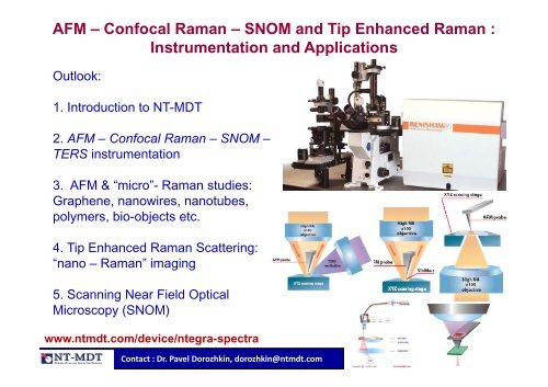
NTEGRA Spectra - NT-MDT
NTEGRA Spectra - NT-MDT
NTEGRA Spectra - NT-MDT

Create successful ePaper yourself
Turn your PDF publications into a flip-book with our unique Google optimized e-Paper software.
<strong>NT</strong>-<strong>MDT</strong> Basic offices modes worldwide<strong>NT</strong>-<strong>MDT</strong> EuropeEindhoven, NL<strong>NT</strong>-<strong>MDT</strong> Head Office,Moscow, Russia<strong>NT</strong>-<strong>MDT</strong> ShanghaiShanghai, China<strong>NT</strong>-<strong>MDT</strong> AmericaSanta Clara, USADistributorsSales Representatives<strong>NT</strong>-<strong>MDT</strong> S&LLimerick, Irelandwww.ntmdt.com
NANOFABsNO<strong>NT</strong>-<strong>MDT</strong> Product lineNanoLabsEducationsAccessories• More than 20 years on the SPM/AFM markety• More than 2400 SPM installations Worldwide• Offices: Moscow, Eindhoven, Limerick, San-Francisco, Shanghai
SPM modes:AFM (contact, intermittent contact), STM
ALL major AFM modes are integrated with RAMAN<strong>NT</strong>-<strong>MDT</strong> Standard Measuring modesMore than 30 possible different AFM modesI<strong><strong>NT</strong>EGRA</strong>TED with Raman-Confocal• STM• Contact AFM• Lateral Force Microscopy• Resonant Mode -Semicontact• Noncontact AFM mode• Phase Imaging• Force Modulation (viscoelastisity)• Magnetic force Microcopy• Electrostatic Force Microscopy• Adhesion Force Imaging• AFM Lithography-Force• Spreading Resistance Imaging (SRI) in Currents 30fA-50nA• AFM Nanolitogrphy (voltage and scratching)• Scanning Capacitance Imaging (SCI) (dC/dZ, dC/dV)• Scanning Kelvin probe microscopy (SKM)• Force distance curves• Force Volume• Nanomanipulation• Piezoresponce Mode• Sample heating for in-situ melting• I/V spectroscopy, I(Z) spectroscopy etc.• Electrochemistryt• SNOM• ….SPM PROBES:- AFM cantilever (any type)- STM- tuning fork (shear force)- tuning fork (normal force)
InvertedUpright
ONE SPM BASEME<strong>NT</strong> & CO<strong>NT</strong>ROLLER –DIFFERE<strong>NT</strong> INSTRUME<strong>NT</strong>SAFM + STMAFM - Confocal Raman -SNOM (UPRIGHT)SNOMAFM - Confocal Raman - SNOM (INVERTED)<strong>NT</strong>-<strong>MDT</strong> SPM’s abilities
<strong><strong>NT</strong>EGRA</strong> <strong>Spectra</strong>Inverted microscope setup (for transparent samples)“AFM + SNOM + 3D confocal Raman microscope + TERS” systemAFM-headRaman unit (<strong>NT</strong>-<strong>MDT</strong>)LasersSample scanning stage(100x,1.4 NA objective inside)<strong><strong>NT</strong>EGRA</strong> universalSPM platformInverted microscope(Olympus, Nikon …)<strong><strong>NT</strong>EGRA</strong> <strong>Spectra</strong>
<strong><strong>NT</strong>EGRA</strong> <strong>Spectra</strong> in Upright setup“AFM + SNOM + 3D confocal Raman microscope + TERS”system for non-transparent samplesRaman unit (Renishaw)Optical AFM-headwith integrated 100x objectiveSample scanner<strong><strong>NT</strong>EGRA</strong> universalSPM platform<strong><strong>NT</strong>EGRA</strong> <strong>Spectra</strong>
Combination of AFM with Raman<strong><strong>NT</strong>EGRA</strong> <strong>Spectra</strong>One object – many techniquesConfocalRaman:imaging andspectroscopyAtomic-forcemicroscopy:mechanical,electrical, magneticproperties p andnanomanipulationsNear-fieldopticalmicroscopyConfocalfluorescence:imaging i andspectroscopyOptical (white light)microscopy andreflected laserconfocal imagingTip Enhanced Raman andFluorescence microscopyMeasurements in air, in liquid or in a controlled environment<strong><strong>NT</strong>EGRA</strong> <strong>Spectra</strong><strong><strong>NT</strong>EGRA</strong> <strong>Spectra</strong>
<strong><strong>NT</strong>EGRA</strong> <strong>Spectra</strong><strong><strong>NT</strong>EGRA</strong> <strong>Spectra</strong>Confocal Raman/Fluorescence - critical resolution
Resolution test: features 200 nm apart are clearly resolvedSample: Mineralic toothpasteResolution: < 200 nmLine #1, Integral intensityRaman map measurement parameters:Objective: 100x, oil immersionLaser: 473 nm, Grating: 150 lines/mmExposure time 0.3 sec<strong>Spectra</strong> per sec: >3Point number: 200x200 pix200 nm300 nm
Very high spectral resolution by Echelle gratingMeasurement parametersLaser: 473 nmObjective: 100x, 0.95 NAGrating: EchelleActual pixels of CCD camera are plotted(26 µm pixel size)<strong>Spectra</strong>l resolution:0281/cm(pixel 0.28 to pixel) for 473 nm laser0.11 1/cm (pixel to pixel) for 785 nm laserSi line, 1 st order
3D Raman mapping, Polystyrene microspheres3D Raman imageX,Y - resolution: 200 nmZ – resolution: 500 nmscan size 10x10x14 µm1010 0 1/cmXY cross-section
<strong><strong>NT</strong>EGRA</strong> <strong>Spectra</strong>Upright configuration for AFM – Confocal Raman – TERSU i i t ti fAFM ithUnique integration of AFM withhigh resolution optical microscopy and spectroscopy
AFM with 100x 0.7 NA objective in upright configuration –for non-transparent samplesCCD video cameraProbedeflectometerOptical AFM head(100x,0.7 NAobjective inside)Imaging opticsBeam splitter 2Beam splitter 1AFM probeExcitation lightScattered lightLaserdeflectometerobjectiveLaserinput&scanningmoduleXYZ scannerNA=0.7400 nm resolutionSample<strong><strong>NT</strong>EGRA</strong> <strong>Spectra</strong>
AFM cantilever under 100x objective (in upright geometry)Cantilever1 µm height letters arereadable – thanks to100x objective(see next slide for AFM)Black spot at the apex ofcantilever is the exactpoint there the tiptouches substrate !!!AFMOptical ImageAFM probe over a structured Si substrate.View through 0.7N 100x objective, resolution 400 nmApex of opaque Si tip looks transparent on the imageThis unique observation is due to high aperture (0.7 NA) of the imaging objective<strong><strong>NT</strong>EGRA</strong> <strong>Spectra</strong>
<strong><strong>NT</strong>EGRA</strong> <strong>Spectra</strong>AFM – Confocal Raman “classical applications”Stress in SiliconSilicon nanowiresCarbon nanotubesGrapheneBio objects…
Mapping stress in Si by spectral shift of 520 cm -1 lineStress distribution around nanoindentation in Silicon substrateScan size: 12x x12 micro on0.5 1/cmAFM topography of indentation insilicon substrateσ(MPa) = -435 ∆ω (1/cm)Center of mass position shift of 520 1/cm siliconline – proportional to stress distribution aroundthe indentation.<strong>Spectra</strong>l resolution: better then 0.1 1/cm<strong><strong>NT</strong>EGRA</strong> <strong>Spectra</strong>
Si nanowire – snapshot from the experimentcantilevercantilevercantilever apexnanowirenanowirelaser spot<strong><strong>NT</strong>EGRA</strong> <strong>Spectra</strong> + Renishaw Raman microscope
Si nanowire - comprehensive characterization in onesample scanOptical imageRaman map (main Si band)Stressed SiAFM topography_____ 5 µm _____ 5 µmRaman map, Si bandcenter of mass positionPristine Si_____ 5 µm _____ 5 µmFluorescence mapRaman map(Si nanoparticles band)_____ 5 µmSi nanoparticles<strong>NT</strong>-<strong>MDT</strong> <strong><strong>NT</strong>EGRA</strong> <strong>Spectra</strong> + Renishaw Raman microscope
Sample: SWCNs, Raman spectrum of nanotube bundleGrating: 600 lines/mmG +Laser: 473 nmRBMDG -2D<strong><strong>NT</strong>EGRA</strong> <strong>Spectra</strong>
Intensity distribution of different Raman bands &AFM topography image of individual <strong>NT</strong> bundleRBM-band D-band G - - band G + - bandAFM height AFM phaseIntegration time: 100 ms / point. 50*150 points.Total spectrum was acquired at each point of the scan. After measurement, different Ramanbands are chosen and their intensity distribution is analyzed. All the images (AFM + all Ramanmaps) can obtained simultaneously, in a single experiment, without any moving of the sampleor objective<strong><strong>NT</strong>EGRA</strong> <strong>Spectra</strong>
Sensing individual SW<strong>NT</strong>s on Si substrate2 nmE (Horizontal pol.)<strong>Spectra</strong>l integration time at 1 point : 100 msecE (vertical pol.)TopographyRaman map (G-band)
<strong><strong>NT</strong>EGRA</strong> <strong>Spectra</strong>AFM – Confocal Raman of Graphene
Graphene, AFM + Confocal RamanOne experiment - multiple dataLateral Force MicroscopyElectrostatic ForceMicroscopyForce Modulation MicroscopyScanning Kelvin ProbeMicroscopyCapacitanceMicroscopyAFM Topography, Size: 30*30 µmRaman Map, G-bandIntensityRaman Map, Mass Center of2D (G’) BandConfocal RayleighMicroscopyData from: E. Kuznetsov,S. Timofeev, P. Dorozhkin, <strong>NT</strong>-<strong>MDT</strong> Co.
HIGH RESOLUTION AFM & STMThe high-resolution AFM image showingan assembly of single-layer,functionalized Graphene sheets.Some of the sheets are many squaremicrometers large. The thickness of eachsheet is less than 1 nm.Atomic resolution STM image of graphite(HOPG)Image courtesy:Dr. Hannes Schniepp (The College of William & Mary, USA)
Light Transport studies with <strong><strong>NT</strong>EGRA</strong> <strong>Spectra</strong>Laser excitation BNanowireFibe er probe(X,Y Y,Z scan)AFM probe (X,Y,Z scan)Detection pointExcitation pointExcitation ti pointsSample (on X,Y,Z-stage)High NA 100x objective(Z-movable)`Emission from endsEmission from endEdge filterLaser excitation ACollected lightX,Y,Z-movable objectiveExcitation pointPinhole: adjustable (0-2 mm) & X,Y-movable<strong><strong>NT</strong>EGRA</strong> <strong>Spectra</strong>To light registration:
Light Transport studies with <strong>NT</strong>egra <strong>Spectra</strong>Emission from endExcitation pointNanowire is locally ll excited at the bottom end. Red curve showsfluorescence spectrum taken at the excitation point. Blue curve is thetransmitted light spectrum taken at the upper end of the nanowire. Greencurve shows spectral transmission function of the nanowire<strong><strong>NT</strong>EGRA</strong> <strong>Spectra</strong>
Beta-carotene distribution in algal cellsOptical image Confocal Laser AFM topographyβ-carotene Raman bandSample courtesy of Don McNaughton,Monash University, AustraliaTail of luminescence(centered at ~630 nm)<strong><strong>NT</strong>EGRA</strong> <strong>Spectra</strong>
Beta-carotene distribution in algal cellsOptical microscope image(with 100x objective)Image size:25x25 µmConfocal laser imageRaman map (ß-carotene) Luminescence map<strong><strong>NT</strong>EGRA</strong> <strong>Spectra</strong>AFM-imageMagnetic-,Kelvin-,Electrostatic-Acoustic Force-Capacitance –Spreading resistance …Scanning Probe images
Malaria infected red blood cell, AFM-RamanAFM topographyRaman mapHemozoin HemoglobinCRaman spectraAFM image of a trophozoite iRBC and a false color 3-cluster UHCA map of the same cell generated fromthe Raman spectra. Mean cluster spectra from the two clusters associated with hemozoin (blue) andhemoglobin (green) are shown. This fixation protocol preserved the structural integrity of the iRBC andsub-micron sized knobs can be seen on the surface of the cell in the AFM image.The size of these knobs were 20-50 nm in height and 100-150 nm in width which is the same as valuespreviously reported and measured by SEM, TEM, and AFM.<strong><strong>NT</strong>EGRA</strong> <strong>Spectra</strong>Data courtesy: Don MacNaughton, Monash Univ.
Polymer sample with protective cover layer - depth profileRaman spectrum versus sample depthample de epth, mSLayer #2Layer #1Zoomed regionRaman shift0.5 mTwo layers are observed.The 2nd layer is 500 nm below the first layerand has a characteristic Raman line (620 cm -1 )<strong><strong>NT</strong>EGRA</strong> <strong>Spectra</strong>
Polymer blendAFM ->Scan size: 40 x 40 µmRaman -><strong>NT</strong>-<strong>MDT</strong> <strong><strong>NT</strong>EGRA</strong> <strong>Spectra</strong> + Renishaw Raman microscope
<strong>NT</strong>-<strong>MDT</strong> + Renishaw I<strong><strong>NT</strong>EGRA</strong>TED systemAdvertising leaflets of the Integrated system (issued by Renishaw and by <strong>NT</strong>-<strong>MDT</strong>)
<strong>NT</strong>-<strong>MDT</strong> + Renishaw I<strong><strong>NT</strong>EGRA</strong>TED software1. Renishaw measurement setupmenu is opened andcontrolled from <strong>NT</strong>-<strong>MDT</strong>NOVA software2. <strong>NT</strong>-<strong>MDT</strong> software FULLYcontrols the AFM-Ramanexperiment (except rareadjustments or calibrations ofthe system)<strong><strong>NT</strong>EGRA</strong> <strong>Spectra</strong>
<strong>NT</strong>-<strong>MDT</strong> + Renishaw I<strong><strong>NT</strong>EGRA</strong>TED softwareEXACTLY THE SAME DATA in two programs: <strong>NT</strong>-<strong>MDT</strong> & Wire-3All scans can be seen and analyzed in any software: AFM (height, phase etc) & Ramanmaps. Data from <strong>NT</strong>-<strong>MDT</strong> Nova was exported into WIRE-3
Tip Enhanced Raman Scattering (TERS)A route to Raman microscopy with subwavelength spatialresolution and single molecule sensitivityTERS – “inverted” SERS effect (scanning metal tip is a HOT SPOT)Metal AFM probeElectromagnetic fieldintensity aroundmetal tip2RR)200-600 nmEnhanced RamansignalFocused laser spot<strong><strong>NT</strong>EGRA</strong> <strong>Spectra</strong>
<strong>NT</strong>-<strong>MDT</strong> provides all possible AFM/Raman/TERS configurationsINVERTED UPRIGHT Side illumination + UPRIGHTTERS collectionexcitationTERS collectionEexcitationexcitationTERS collectionDifferent probe types and feedback mechanisms:AFM (contact, intermittent contact), STM, Tuning fork (normal force and shear force)Dual scan: 6 piezodriven coordinates (“laser + sample” or “tip + sample”)
Tip Enhanced RamanINVERTED geometry (transparent samples)Shear force
To find HOT POI<strong>NT</strong> (Maximum enhancement):Scan - BY TIP; Measure - intensity of laser light scattered by the tipMetal AFM probexy&z-scanx,y EFocused laser spotHot point !1. Scan (XY&Z) by tip acrossthe laser spot.Measure Raman or Rayleighscattered light2. Position tip inside “hot point”with high precision200 nm ____Etched Au wireScan by the sample to getTERS mapData courtesy of S. Kharintsev, J. Loos, G. Hoffman, G. de With, TUE, the Netherlands and P. Dorozhkin, <strong>NT</strong>-<strong>MDT</strong>
TERS imaging of single-walled C<strong>NT</strong> bundle__ 200 nmTip is awayTube image widthAFM topography(height is ~250ht ~ 5 nm nm)(limited bywavelength of light)200 Raman map(G-line)__ 200 nmTip is approachedLaser: 633 nmTube image width isTip: Etched gold wire ~50 nm (limited(only by size of the tip)S.S. Kharintsev, G. Hoffmann, P.S. Dorozhkin,G. de With, and J. LoosNanotechnology 18 (2007), 315502Raman spectra and 2D confocal Raman maps (G-line) of carbon nanotuberope with and without enhancing AFM tip (GOLD wire)<strong><strong>NT</strong>EGRA</strong> <strong>Spectra</strong>
TERS with Silver coated cantileversScan size: 2x3 micronAFM image of carbon nanotubebundleTERS image of the samebundleImage courtesy: Jacon Jao, Renato Zenobi ETH Zurich, Switzerland; G.Hoffman, J. Loos, TUE, Eindhoven; and Pavel Dorozhkin, <strong>NT</strong>-<strong>MDT</strong> Russia<strong><strong>NT</strong>EGRA</strong> <strong>Spectra</strong> `
Tip Enhanced RamanUPRIGHT geometry (non-transparent t samples)100x0.7 NATERS excitationTERS collection100xTERS collection 0.7 NAE0.7 NAexcitation45°
Looking for Hot Spot –laser beam is scanned across the cantilever0.7 NA45°Laser scanning module allows to position laser beam precisely at the apex of AFMtip and fix it there - thanks to closed-loop operation of the scanning mirror
TERS in UPRIGHT geometry – GrapheneFinding HOT SPOT on AFM tipRaman spectra from Graphene flake:cantilever--- Inside “hotspot”--- Outside “hotspot”--- Signal from tip (sample is removed)Data from: A. Schokin &P. Dorozhkin, <strong>NT</strong>‐<strong>MDT</strong>Laser beam is scanned across cantilever tipRaman signal from substrate measured
TERS on periodic Si-Ge structure, resolution ~50 nmData courtesy: Dr. Peter Hermann et at., Fraunhofer C<strong>NT</strong> & AMD, DresdenTERS tool evaluation project, AMD Dresden & <strong>NT</strong>-<strong>MDT</strong>
Successful Tip Enhanced Raman experiment:Major requirements to experimental setup (AFM – Raman combination)1. Different geometry of AFM and high resolution Raman optics: bottomillumination/collection, top illumination/collection, side illumination/ topcollection.2. Dual scan option (6 closed loop piezo coordinates): sample+laserscanning OR sample+tip scanning3. All AFM and Raman control must be integrated into one software package4. Very low AFM noise (to keep TERS tip safely veryclose to sample), low drifts and high stability(to keep laser exactly on the hotspot – with 10 nm precision)5. Good TERS tip
SCANNING NEAR-FIELD OPTICAL MICROSCOPYStraight quartz fiber withaperture (glued to tuning fork)Silicon cantilevers withaperture100x, 0.7 NAAll SNOM modes are available:Collection, Transmission, Reflection(for all signals/modes: laser, fluorescence and spectroscopy)
AUTOMATIC alignment of laser spot and SNOM aperturelaser spot is scanned: x,yIntensity of light transmittedthrough cantileverPrecise location of SNOM aperture___ 10µmLaser spot is scanned in automatic regime across SNOM cantilever and transmittedsignal is measured – to locate the SNOM aperture with very high accuracy (
SNOM transmission: Single lipofuscin granuleShear force topographySNOM transmissionSingle lipofuscin granule 400 nm in height and 1.7 – 2.7 µm indiameter. Two “humps” can be seen as well at shear-force image(left one). On the right image transmission at 420 nm can be seen.Quartz substrate transmission was subtracted so negative values canbe referred to sample absorption and positive ones (most probably)to sample fluorescence.<strong><strong>NT</strong>EGRA</strong> <strong>Spectra</strong>
SNOM spectroscopy: Single lipofuscin granulePoint-localized spectroscopy of putative fluorescent region. Thespectrum obtained corresponds well with the spectrum of pureA2E fluorophore thought to be the major cause of aging-relatedretina degeneration.<strong><strong>NT</strong>EGRA</strong> <strong>Spectra</strong>
SNOM on photonicSNOM Lithographycrystalperformanceoptical fibersOverlay of simultaneously measured:Sample topography (orange/red palette) andSNOM intensity (green palette)<strong><strong>NT</strong>EGRA</strong> <strong>Spectra</strong>Data courtesy:Yinlan Ruan, Heike Ebendorff-Heidepriem, Tanya M. MonroCentre of Expertise in Photonics, School of Chemistry &Physics, University of Adelaide, Adelaide, 5000 Australia
SNOM measurements (VIS & IR) : Cr:YAG optical fibers
SNOM on Surface Plasmon PolaritonsData from:Antonell Nesci and Olivier J.F. Martin,EPFL, Lausanne, Switzerland
SNOM on Surface Plasmon PolaritonsData from:Antonell Nesci and Olivier J.F. Martin,EPFL, Lausanne, Switzerland
<strong><strong>NT</strong>EGRA</strong> <strong>Spectra</strong><strong><strong>NT</strong>EGRA</strong> <strong>Spectra</strong>AFM – Raman – SNOM in controlled environment
AFM + Raman + SNOM in LIQUIDSNOMAFM<strong>NT</strong>-<strong>MDT</strong> Closed-liquid cell with heatingPossible to use with AFM + SNOM + Confocal Raman (Confocalfluorescence), work with living cells. Flow-trough possibility.WORKS WITH AFM/SNOM/ RAMAN (INVERTED)<strong><strong>NT</strong>EGRA</strong> <strong>Spectra</strong>
AFM – Raman – SNOM in Upright configuration in liquid100x100xNA = 1NA = 1280 nm280 nm2 mm- NA=1 (120º)- TERS in liquid for opaque samples- Cantilever based SNOM in liquid
Electrochemical cell for AFM – Raman in external magnetic fieldAFM quartz noseEC cellEC cellTransparent sampleCantileverobjectiveobjective• Microscope configuration: Inverted• Objectives used: any objective (Olympus,Nikon)• AFM modes in liquid: contact, noncontact• Sample: transparent (ITO, quartz withthin metal layer etc.)• Stabilized temperature (-10º - +60º)• External magnetic field (up to 0.2 T)<strong><strong>NT</strong>EGRA</strong> <strong>Spectra</strong>
Ultra Stable AFM – Confocal Raman – TERS measurementsin wide temperature range3000Raman spectra of Grapheneflake at T = -20, +20, +80 ºC2750250022502000Raman spectrums vs temperatureT=25 CT= 80 CT= -20 CCou unts175015001250T = -30 - +80 ºCDrifts < 10 nm per 1ºC< 10 nm per hour at all temperatures100075050012001400 1800 2200 2600 30001600 2000 2400 2800 3200Raman shift, cm-1
AFM-Raman-SNOM-TERS in CO<strong>NT</strong>ROLLED ATMOSPHEREControlled atmosphere chamber for AFM-Raman-TERS(controlled temperature, humidity, inert gases etc.)<strong><strong>NT</strong>EGRA</strong> <strong>Spectra</strong>
Modes<strong>NT</strong> <strong>MDT</strong> integratesAFM, SNOM, Confocal Raman/Fluorescence and TERSin one deviceControlled environment• AFM (mechanical, electrical, magnetic propertiesand nanomanipulation – more than 30 modes)• White Light Microscopy and Reflected Laser(Rayleigh) Confocal Imaging• Confocal Raman Imaging and Spectroscopy• Confocal Fluorescence Imaging g andSpectroscopy• Scanning Near-Field Optical Microscopy•Temperature•Humidity•Gases•Liquid•Electrochemical environment•External magnetic field• Tip Enhanced Raman and FluorescenceMicroscopy (TERS, TEFS)www.ntmdt.com/device/ntegra-spectraContact : Dr. Pavel Dorozhkin, dorozhkin@ntmdt.com