A New Scanning Method for Fast Atomic Force Microscopy - NT-MDT
A New Scanning Method for Fast Atomic Force Microscopy - NT-MDT
A New Scanning Method for Fast Atomic Force Microscopy - NT-MDT

You also want an ePaper? Increase the reach of your titles
YUMPU automatically turns print PDFs into web optimized ePapers that Google loves.
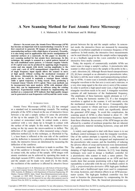
This article has been accepted <strong>for</strong> publication in a future issue of this journal, but has not been fully edited. Content may change prior to final publication.1A <strong>New</strong> <strong>Scanning</strong> <strong>Method</strong> <strong>for</strong> <strong>Fast</strong> <strong>Atomic</strong> <strong>Force</strong> <strong>Microscopy</strong>I. A. Mahmood, S. O. R. Moheimani and B. BhikkajiAbstract—In recent years, the <strong>Atomic</strong> <strong>Force</strong> Microscope (AFM)has become an important tool in nanotechnology research. It wasfirst conceived to generate 3D images of conducting as well asnonconducting surfaces with a high degree of accuracy. Presently,it is also being used in applications that involve manipulation ofmaterial surfaces at a nanoscale. In this paper we describe anew scanning method <strong>for</strong> fast atomic <strong>for</strong>ce microscopy. In thistechnique, the sample is scanned in a spiral pattern instead ofthe well established raster pattern. A Constant Angular Velocity(CAV) spiral scan can be produced by applying single frequencycosine and sine signals with slowly varying amplitudes to thex-axis and y-axis of AFM nanopositioner respectively. The useof single frequency input signals allows the scanner to moveat high speeds without exciting the mechanical resonance ofthe device. Alternatively, the frequency of the sinusoidal setpointscan be varied to maintain a constant linear velocitywhile a spiral trajectory is being traced. Thus, producing aConstant Linear Velocity (CLV) spiral. These scan methods canbe incorporated into most modern AFMs with minimal ef<strong>for</strong>tsince they can be implemented in software using the existinghardware. Experimental results obtained by implementing themethod on a commercial AFM indicate that high-quality imagescan be generated at scan frequencies well beyond the raster scans.I. I<strong>NT</strong>RODUCTION<strong>Atomic</strong> <strong>Force</strong> Microscope (AFM) [1], [2] has emergedas a standard tool in nanotechnology research. The workingprinciple of the AFM is based on the use of interactive <strong>for</strong>cesbetween a tip and a sample surface to sense the proximityof the tip to the sample [3]. The AFM can be used eitherin contact or noncontact mode. In contact mode, a microcantileverwith a very sharp tip is brought in contact withthe surface of the sample. In this mode, the repulsive <strong>for</strong>ceacting on the tip causes the micro-cantilever to deflect. Thedeflection of the cantilever is often measured using a beamdeflectionmethod [2]. In this technique, as illustrated in Fig.1, a laser beam is reflected at the rear side of the cantileverand the deflection is measured by a photodetector. In contactmode, the interactive <strong>for</strong>ces are determined by measuring thedeflection of the cantilever.In noncontact mode the cantilever is made to oscillate. Thetip of the cantilever is brought close to, but without comingin contact with, the surface of the sample. AFM images withatomic resolution can be achieved by operating this mode inultra-high vacuum (UHV), where the distance between the tipand the sample can be made very small [3]. In this mode,the oscillation of the cantilever is affected by attractive <strong>for</strong>cesI. A. Mahmood and S. O. R. Moheimani are with School of Electrical Engineeringand Computer Science, The University of <strong>New</strong>castle, Callaghan, NSW2308, Australia. B. Bhikkaji is with Department of Electrical Engineering, IITMadras, Chennai 600036, India. Email: Reza.Moheimani@newcastle.edu.au.Copyright (c) 2009 IEEE. Personal use of this material is permitted.However, permission to use this material <strong>for</strong> any other other purposes must beobtained from the IEEE by sending a request to pubs-permissions@ieee.org.present between the tip and the sample surface. In noncontactmode, the interactive <strong>for</strong>ces are measured by measuringchanges in oscillation amplitude or resonance frequency of thecantilever. In both modes, the interactive <strong>for</strong>ce measurementscan be used directly to generate the sample surface topographyor as a feedback signal to the z-axis controller to keep theinteractive <strong>for</strong>ce nearly constant.Today, the majority of commercially available AFMs useraster scans to image a sample’s surface. A piezoelectric tubescanner is often used to move the sample or the probe in the x,y and z directions [4]. Although flexure-based nanopositioners[5], [6] have emerged as an alternative to piezoelectric tubes,the latter is still the most widely used nanopositioning technologyin AFMs. A raster scan is normally attained by applying atriangular wave<strong>for</strong>m to the fast axis (x-axis) and a staircase, ora very slow ramp signal to the slow axis (y-axis) of the scanner.In order to per<strong>for</strong>m a high-speed raster scan, a high frequencytriangular wave<strong>for</strong>m needs to be used. A triangular wave<strong>for</strong>mcontains all odd harmonics of the fundamental frequency.The amplitudes of these harmonic signals attenuate as 1/n 2 ,with n being the harmonic number [7]. If a fast triangularwave<strong>for</strong>m is applied to the scanner, it will inevitably excitethe mechanical resonance of the device. Consequently, thiscauses the scanner to vibrate and trace a distorted triangularwave<strong>for</strong>m along the x-axis which can significantly distortthe generated AFM image. To avoid this complication, thescanning speed of AFMs is often limited to about 10 - 100times lower then the scanner’s first resonance frequency. Apartfrom these vibrations, the accuracy of the AFM images are alsoaffected by a number of nonlinear properties that are inherentto piezoelectric material including hysteresis, creep and drift[8], [9].A widely used approach to deal with these issues is to usefeedback control techniques to track the triangular wave<strong>for</strong>m.One of the earliest attempts is reported in [10], where Lagleadand H ∞ controllers were designed and implemented onthe piezoelectric tube scanner, and the feasibility of reducingthe adverse effects of creep and hysteresis were demonstrated.The authors also reported that the H ∞ controller achieveddamping of high-frequency vibrations. In [11], loop shapingtechniques were used to design a feedback controller <strong>for</strong>a piezoelectric tube scanner to track a raster pattern. Theclosed-loop system was implemented on an AFM and theirresults show that accurate positioning with a high degree ofrepeatability is achievable with the use of feedback control. In[12], a proportional-plus-derivative (PD) high-gain feedbackcontroller and a feed<strong>for</strong>ward input were used to compensate<strong>for</strong> creep, hysteresis, and vibration effects in an AFM piezoactuatorsystem. The high-gain feedback controller was firstused to linearize the piezoactuator by compensating <strong>for</strong> thecreep and hysteresis. Then, the linearized piezoactuator wasCopyright (c) 2009 IEEE. Personal use is permitted. For any other purposes, Permission must be obtained from the IEEE by emailing pubs-permissions@ieee.org.Authorized licensed use limited to: University of <strong>New</strong>castle. Downloaded on November 26, 2009 at 00:02 from IEEE Xplore. Restrictions apply.
This article has been accepted <strong>for</strong> publication in a future issue of this journal, but has not been fully edited. Content may change prior to final publication.2Figure 1.z-axiscontrollerx, y-axiscontrollerSample-1-1Piezoelectric tubescannerPhotodetectorLaserBasic AFM schematic with feedback controllers.Micro-cantileverTipx, y positionsensorsmodeled to determine the feed<strong>for</strong>ward input to account <strong>for</strong> thevibration effects. Their results indicated that the inclusion offeed<strong>for</strong>ward input reduces the tracking error more as comparedto using only feedback control. Other examples of successfulapplications of feedback control techniques include [13]–[17]. An exhaustive review of the literature can be found inreference [9].The use of feedback controllers in damping and linearizingthe piezoelectric tube scanner has been shown to be successfulin the above mentioned works [10]–[17]. However,these feedback controllers have little success in tracking highfrequency triangular wave<strong>for</strong>ms. Closed-loop tracking of thesewave<strong>for</strong>ms typically results in the corners of the triangularwave<strong>for</strong>m to be rounded off. This is due to the presenceof high frequency harmonics that are inevitably outside ofthe bandwidth of the closed-loop system. Consequently, AFMimages generated at high speeds often demonstrate significantdistortions especially around the edges of the image.This paper proposes a new scan technique <strong>for</strong> fast atomic<strong>for</strong>ce microscopy by <strong>for</strong>cing the scanner to follow a spiraltrajectory over the surface that is to be imaged. A constant angularvelocity (CAV) spiral scan can be produced by applyingslowly varying-amplitude single frequency sinusoidal signalsto the x- and y-axes of the piezoelectric tube scanner. The useof the single frequency input signals allows <strong>for</strong> scanning to beper<strong>for</strong>med at very high speeds without exciting the resonanceof the scanner and with relatively small control ef<strong>for</strong>ts. Analternative method is to generate the spiral pattern in a constantlinear velocity (CLV) approach. The latter method has beenimplemented in some disk storage devices, such as CompactDisk-Read Only Memory (CD-ROM) where the in<strong>for</strong>mationis stored in a continuous spiral track over the disk’s surface[18]. The proposed method is an alternative to raster-basedsinusoidal scan methods that are used to achieve fast scans ine.g., scanning near-field optical microscopy (SNOM) [19]. Inspiral scanning, both axes follow sinusoidal signals of identicalfrequencies resulting in a smooth trajectory. This avoids thetransient behavior that may occur in sinusoidal scans as theprobe moves from one line to the next. Furthermore, theproposed method does not require specialized hardware, e.g.a tuning <strong>for</strong>k actuator, and can be implemented on a standardAFM with minor software modifications.It should be noted that recently a few prototype laboratoryAFMs have been developed that are capable of imaging asample at, or close to, video-rates, [20]–[23]. Such a functionalityis particularly useful in a number of applications, e.g.when capturing the dynamic behavior of certain biomolecularprocesses is needed. In order to achieve video rates, using araster scanned AFM, the scan frequency has to be quite high,close to 5 kHz or higher. The spiral scanning method proposedin this paper may be a good candidate <strong>for</strong> such applications.This scheme can be easily implemented on a commercial,or prototype AFM, with minimal software modifications. Itshould be pointed out that to operate an AFM at such high scanfrequencies one has to overcome other technical challenges,such as the need to utilize very small micro-cantilevers withextremely high resonance frequencies [20].The remainder of this paper is organized as follows. Thegeneration of input signals to produce the spiral pattern is describedin detail in Section II. Section III provides descriptionsof the AFM and other experimental setups used in this work.Modeling and identification of the system transfer functionsare presented in Section IV. Control schemes <strong>for</strong> the AFMscanner are devised in Section V. In Section VI experimentalresults are presented to illustrate the drastic improvement inimaging speed that can be achieved with the proposed newscan trajectory. Finally, Section VII concludes the paper.II. SPIRAL SCA<strong>NT</strong>his section deals with the generation of input signals thatare needed to move the AFM scanner in a spiral pattern,illustrated in Fig. 2. The pattern is known as the Archimedeanspiral. A property of this spiral is that its pitch P, which isdistance between two consecutive intersections of the spiralcurve with any line passing through the origin, is constant[24]. Depending on how this trajectory is traced, the shape isreferred to as either a Constant Angular Velocity (CAV) spiral,or a Constant Linear Velocity (CLV) spiral. In the <strong>for</strong>mer case,the pattern is traced at a constant angular velocity, while inthe latter at a constant linear velocity.A. The CAV spiralThe equation that generates a CAV spiral of pitch P atan angular velocity of ω can be derived from a differentialequation given in [18] asdrdt = Pω(1)2πwhere r is the instantaneous radius at time t. Equation (1) issolved <strong>for</strong> r by integrating both sides to obtain∫dr = Pω ∫dt. (2)2πFor r = 0 at t = 0,r = P ωt. (3)2πHere, P is calculated asspiral radius × 2P = (4)number o f curves − 1Copyright (c) 2009 IEEE. Personal use is permitted. For any other purposes, Permission must be obtained from the IEEE by emailing pubs-permissions@ieee.org.Authorized licensed use limited to: University of <strong>New</strong>castle. Downloaded on November 26, 2009 at 00:02 from IEEE Xplore. Restrictions apply.
This article has been accepted <strong>for</strong> publication in a future issue of this journal, but has not been fully edited. Content may change prior to final publication.363Pxs (µm)6303(a)ys (µm)0361 2 3 4 5 6 76 3 0 3 6x s (µm)Figure 2. Spiral scan of 6 µm radius with number o f curve = 8.where number o f curves is defined as the number of timesthe spiral curve crosses through the line y = 0. This isexemplified in Fig. 2 where the crossing points are numbered.The figure illustrates a spiral scan of 6 µm radius withnumber o f curves = 8.The equation that describes the total scanning time t total associatedwith a CAV spiral scan can be derived by integratingboth sides of equation (1) as∫r end∫t enddr = Pω dt (5)2πr start t startwhere r start and r end are initial and final values of the spiralradius, and t start and t end are initial and final values of thescanning time. From equation (5), if r start = 0 at t start = 0 andt total = t end −t start , we obtaint total = 2πr endPω . (6)In order to implement the spiral scans using a piezoelectrictube scanner, equation (3) needs to be translated into cartesiancoordinates. The trans<strong>for</strong>med equations areandx s = r cosθ (7)y s = r sinθ (8)where x s and y s are input signals to be applied to the scanner inthe x and y axes respectively and θ is the angle. From ω =dt dθ ,θ is obtained as θ = ωt. An example of input signals x s andy s that can generate the spiral in Fig. 2 is plotted in Fig. 3.The figure illustrates constant phase errors between the inputsignals and measured outputs. Such errors are due to the nonidealfrequency response of the controlled nanopositioner. Fora CAV spiral, these phase errors can be easily eliminated byadding phase constants α x and α y to shape the input signalsasX s = r cos(θ + α x ) (9)andY s = r sin(θ + α y ). (10)8ys (µm)60 0.04 0.08 0.12t (s)(b)630360 0.04 0.08 0.12t (s)Figure 3. Input signals to be applied to the scanner in the x and y axes ofthe scanner to generate CAV spiral scan with ω = 188.50 radians/sec. Solidline is the achieved response and dashed line is the desired trajectory.Here, α x and α y are determined by measuring the closed-loopfrequency response of the system at the scan frequency. Theymay also be determined off-line if a model of the system isat hand.A key advantage of using a CAV spiral is that closed-looptracking of this pattern when implemented via the cartesianequations only involves tracking single frequency sinusoidalsignals with slowly varying amplitudes. This advantage, whencombined with the use of the shaped input signals (9) and (10),enables the AFM’s scanner to track a high frequency CAVspiral resulting in fast atomic <strong>for</strong>ce microscopy. A drawbackof this method is that its linear velocity v is not constant. Thus,it may not be suitable <strong>for</strong> scanning some samples where theinteraction between the probe and the sample needs to be doneat linear velocity. The CLV spiral presented next overcomesthis problem.B. The CLV spiralIn order to generate a CLV spiral, the radius ˜r and angularvelocity ˜ω need to be varied simultaneously in a way thatthe linear velocity of the nanopositioner is kept constant atall times. The expressions <strong>for</strong> ˜r and ˜ω are first derived bysubstituting ω = v rinto equation (1) to obtaindrdt = Pv(11)2πrwhere v is the linear velocity of the CLV spiral. Then, equation(11) is solved <strong>for</strong> r by integrating both sides of the equationas∫rdr = Pv ∫dt. (12)2πFor r = 0 at t = 0, we obtain√Pv˜r = t. (13)πFrom equation (13), by substituting ˜r = ṽ the expression <strong>for</strong>ω˜ω is obtained as √πv˜ω =Pt . (14)Copyright (c) 2009 IEEE. Personal use is permitted. For any other purposes, Permission must be obtained from the IEEE by emailing pubs-permissions@ieee.org.Authorized licensed use limited to: University of <strong>New</strong>castle. Downloaded on November 26, 2009 at 00:02 from IEEE Xplore. Restrictions apply.
This article has been accepted <strong>for</strong> publication in a future issue of this journal, but has not been fully edited. Content may change prior to final publication.4It is worth noting that ˜r and ˜ω are non-linear functions of time,and ˜ω approaches infinity at t = 0. For practical reasons duringdigital implementation of the CLV spiral, t = 0 is approximatedwith t = sampling period of the digital system.The equation <strong>for</strong> total scanning time ˜t total of a CLV spiralscan can be derived in a similar manner to the CAV spiral.From equation (11), ˜t total is derived as˜t total = πr2 endPv . (15)By choosing v = ˜ω end r end where ˜ω end is the instantaneousangular velocity at r end , the equation <strong>for</strong> ˜t total can be rewrittenas˜t total = πr endP˜ω end. (16)It can be inferred from equation (16) that if ˜ω end = ω, the totalscanning time of a CLV spiral is half of the total scanning timeof a CAV spiral. This makes the CLV spiral a more attractiveoption. However, as we will see later, this gain in scanningtime comes at the expense of introducing distortion at thecenter of the AFM image.Similar to the CAV spiral, equation (13) can be describedin cartesian coordinates asand˜x s = ˜r cos ˜θ (17)ỹ s = ˜r sin ˜θ (18)where ˜θ <strong>for</strong> time varying ˜ω is obtained as√4πv˜θ = t. (19)PFig. 4 illustrates the input signals ˜x s and ỹ s that can be used togenerate a spiral similar to the one shown in Fig. 2. However,as illustrated in the figure, the input signals are implementedin a reversed order, that is from r end to r start . To generate aCLV spiral, that starts from ˜r = 0, one requires a closed-loopsystem with extremely high bandwidth (ideally ∞ bandwidth)and a closed loop system with a flat phase and magnituderesponse. This of course, is not practical. Thus, if the spiral isstarted from ˜r = 0, the initial error that is inevitably generatedwill propagate all the way through to the end. In the nextsection, we propose an inversion algorithm that can minimizethe tracking error arising from the limited bandwidth and nonidealfrequency response of the closed loop system.C. Inversion Technique <strong>for</strong> CLV spiralIn this section a technique to shape inputs such that theresulting trajectory will be a CLV spiral with minimal trackingerror is presented. As the implementation of the entire schemewill be in discrete time, the input shaping method presentedhere is also described in discrete time.The goal is to design input signals {u x [k]} N k=0 and{uy [k] } Nsuch that their outputs, along the x and y axes are,k=0{x[k] = ˜x(kT)} N k=0 and {y[k] = ỹ(kT)}N k=0 respectively. Here,T denotes the sampling interval and ˜x and ỹ are as definedin equations (17) and (18). In the following only designing˜xs (µm)ỹs (µm)630360 0.02 0.04 0.06t (s)(b)6303(a)60 0.02 0.04 0.06t (s)Figure 4. Input signals to be applied to the scanner in the x and y axes ofthe scanner to generate CLV spiral scan with v = 1.13 mm/sec (or ˜ω end =188.50 radians/sec). Solid line is the achieved response and dashed line is thedesired trajectory.of {u x [k]} N k=0 will be described, with the understanding that{uy [k] } Ncan be generated by adopting the same procedure.k=0Assume that the transfer function relating the input and theoutput along the x direction is given byG x (z) =b 0 + b 1 z −1 + b 2 z −2 +...+b m z −m1+a 1 z −1 + a 2 z −2 , (20)+...+a m z−m which is stable but has non-minimum phase zeros, i.e. all ofzeros are outside the unit circle. As G x (z) is non-minimumphase, a direct inversion is not possible. Furthermore, as ˜xand ỹ are not periodic, a frequency domain inversion of thetype presented in [15] will not be accurate.Note that equation (20) in the discrete time corresponds tothe difference equationThis impliesx[n]+a 1 x[n − 1]+...+a m x[n − m]= b 0 u x [n]+b 1 u x [n − 1]+...+b m u x [n − m]. (21)u x [n − m] = 1b m(x[n]+a 1 x[n − 1]+...+a m x[n − m]−b n u x [n] −... − b m−1 u x [n −(m − 1)]). (22)As {x[k]} N k=0 is given, assuming arbitrary values <strong>for</strong>u x [N],u x [N −1],...,u x [N −(m−1)], the input sequence u x [N −(m−1)],u x [N −(m−2)],...,u x [1],u x [0] can be calculated fromequation (22). As an example consider m = 2 in (21). Thisimpliesandx[n]+a 1 x[n − 1]+a 2 x[n − 2]= b 0 u x [n]+b 1 u x [n − 1]+b 2 u x [n − 2] (23)u x [n − 2] = 1 b 2(x[n]+a 1 x[n − 1]+a 2 x[n − 2] − b 0 u x [n] − b 1 u x [n − 1]). (24)Copyright (c) 2009 IEEE. Personal use is permitted. For any other purposes, Permission must be obtained from the IEEE by emailing pubs-permissions@ieee.org.Authorized licensed use limited to: University of <strong>New</strong>castle. Downloaded on November 26, 2009 at 00:02 from IEEE Xplore. Restrictions apply.
This article has been accepted <strong>for</strong> publication in a future issue of this journal, but has not been fully edited. Content may change prior to final publication.5Setting u x [N] and u x [N − 1] to arbitrary values, u x [N − 2]can be back calculated from equation (24). Similarly, usingthe calculated u x [N − 2] and the arbitrarily chosen u x [N − 1],u x [N −3] can be computed. Thus, traversing backwards in timeone can compute u x [n] up to n = 0.The above mentioned procedure can be proved to be stable,and can be shown to converge to an input sequence that wouldgenerate the output ˜x(kT). However, the proof is beyond thescope of this paper. If a user has to deal with a continuoustime transfer function G x (s), he or she could approximateit by a discrete transfer function G x (z) using the bilineartrans<strong>for</strong>mation or any other approximation technique.D. Total scan time: Spiral scan vs. Raster scanA fair comparison of the total scanning time <strong>for</strong> spiral andraster scans can be made by evaluating the time required <strong>for</strong>both methods to generate images of equal areas and pitchlengths. The area of a circular spiral scanned image A spiralwith a radius of r end can be calculated asA spiral = πr 2 end . (25)The area of a rectangular raster scanned image A raster can becalculated usingA raster = L 2 (26)where L is length of the square image. For both images to havean equal area, equations (25) and (26) are equated to obtainL = √ πr end . (27)The number of lines in a raster scanned image with pitch Pcan be calculated asnumber o f lines = L + 1. (28)PThe total scan time to generate a raster scanned image can beobtained usingt total raster =number o f linesf(29)where f is the scan frequency. Thus, by substituting equations(27) and (28) into equation (29), the total scan time <strong>for</strong>generating a raster scanned image with an area of πrend 2 canbe determined ast total raster =√πrendP f+ 1 f . (30)The total scanning time to generate a spiral scanned imagein a CAV mode can be calculated using equation (6) and bysubstituting ω = 2π f into equation (6),t total = r endP f . (31)It can be deduced from equations (30) and (31), by ignoringthe term 1 fin equation (30), <strong>for</strong> the same scan frequency, animage of equal area and pitch can be generated √ π (≈ 1.77)times faster using a CAV spiral scan than a raster scan.In order to compare the total scanning time <strong>for</strong> a CLV spiralscan and a raster scan, the linear velocity of the raster scanv r = 2L f is introduced into equation (30) to obtainedt total raster = 2πr2 endPv r(32)with the term 1 fignored. It can be deduced from equations(32) and (15), <strong>for</strong> the same linear velocity, v r = v, an imageof equal area and pitch can be generated two times faster usinga CLV spiral scan than a raster scan.E. Total trajectory distance : Spiral scan vs. Raster scanIn this section, total trajectory distance in generating imagesof equal area and pitch length using spiral and raster scans arecompared. The total trajectory distance of a spiral scan s spiralcan be derived from equation (15) ass spiral = πr2 endP . (33)Note that, (33) also holds <strong>for</strong> a CAV spiral scan.The total trajectory of a raster scan s raster can be written ass raster = 2L × number o f lines. (34)By substituting equations (28) and (27) into equation (34),s raster can be obtained ass raster = 2πr2 end+ 2 √ πr end . (35)PIt can be deduced from equation (35) and (33) that, s raster isat least two times longer than s spiral . An immediate advantageof this is that, there will be less wear on the AFM tip whenthe spiral scan is used instead of the raster scan.F. Mapping Spiral Points to Raster PointsIn this work, the spiral-scanned images are plotted bymapping the sampling points along the spiral trajectory (called“spiral points”) to points or pixels (called “raster points”) thatmake up a raster-scanned image placed on top of the spiralpoints as shown in Fig. 5 (a) and (b) <strong>for</strong> CAV and CLV spiralsrespectively. A major advantage of mapping the spiral pointsto the raster points is that it allows the user to utilize existingimage processing software developed specifically <strong>for</strong> rasterscannedimages, to plot the generated spiral image.In this mapping procedure, the dimension of the rasterscannedimage is set to spiral diameter × spiral diameterwhere the spiral diameter ≈ spiral radius × 2, and the pitchof the raster-scanned image is chosen to be equal to thepitch P of the spiral. Consequently, the number of lines inthe raster-scanned image will be equal to the number ofcurves in the spiral trajectory. Then, each raster point locatedwithin the spiral radius is mapped to the nearest spiral point.Since position of the raster and spiral points are known <strong>for</strong>any scan frequency and dimension, the nearest spiral pointcorresponding to each raster point can be identified and storedin an indexed matrix be<strong>for</strong>e per<strong>for</strong>ming the sample scans. Bydoing this, the image of the sample can be plotted in real-time,i.e., as the AFM is scanning the sample.Copyright (c) 2009 IEEE. Personal use is permitted. For any other purposes, Permission must be obtained from the IEEE by emailing pubs-permissions@ieee.org.Authorized licensed use limited to: University of <strong>New</strong>castle. Downloaded on November 26, 2009 at 00:02 from IEEE Xplore. Restrictions apply.
This article has been accepted <strong>for</strong> publication in a future issue of this journal, but has not been fully edited. Content may change prior to final publication.7+yA/DdSPACE1103D/Aux, uxcx, cxChargeamplifiers+x −xSAMCapacitivesensorsPiezoelectrictubeScannerFigure 7. Top view of the piezoelectric tube with the internal and externalelectrode wired in a bridge configuration.feedback control. In these experiments, a closed-loop scanner<strong>NT</strong>-<strong>MDT</strong> Z50309cl was used to per<strong>for</strong>m 3D positioning inthe SPM. It has a scanning range of 100 × 100 × 10 µm.The capacitive sensors that are incorporated into the scannerapparatus allow <strong>for</strong> direct measurements of the scanner displacementin x, y and z axes. The bandwidth of these capacitivesensors is tunable and has a maximum value of 10 kHz. Inthese experiments the bandwidth is set to the maximum inorder to minimize the effect of the capacitive sensors dynamicson the displacement measurements. The sensitivity of thecapacitive sensors was determined by making the scanner tracka 0.5 Hz triangular wave of 100 µm amplitude in closed-loopusing the standard <strong>NT</strong>-<strong>MDT</strong> SPM controller. Simultaneously,the corresponding output voltages from the capacitive sensorswere also measured. From these two values, the sensitivity ofthe capacitive sensors incorporated into the x and y axes wascalculated to be 6.33 µm/volt. In this test, a low frequencytriangular wave was used to ensure perfect tracking by thestandard <strong>NT</strong>-<strong>MDT</strong> SPM controller.The piezoelectric tube in the scanner has quartered internaland external electrodes. Such electrode arrangement allowsthe scanner to be driven in a bridge configuration [26] wherethe electrodes are wired in pairs as illustrated in Fig. 7. Theseelectrode pairs are referred to as +x, −x, +y and −y electrodepairs. An advantage of using the bridge configuration is thatit halves the input voltage requirement as compared to themore widely-used grounded internal electrode configuration.Nevertheless, in these experiments the −x and −y electrodesare grounded in order to simplify the experimental setup.Furthermore, the need <strong>for</strong> a large scanning range does notarise here since the scanner is only made to operate within12 % of its full lateral scanning range.During scans, measurements from the capacitive sensors andphotodiode are recorded and processed in Matlab to generateAFM images.−yIV. SYSTEM IDE<strong>NT</strong>IFICATIONIn this section, the procedure used to model the AFM scanneris described. The scanner is treated as a two single-inputsingle-output (SISO) systems in parallel. The inputs being theFigure 8. Block diagram of the experimental setup used <strong>for</strong> systemidentification of the scanner.voltage signals applied to the charge amplifiers driving +xelectrode pair, u x and +y electrode pair, u y . The outputs ofthe system are the scanner displacement measurements fromthe capacitive sensors in x-axis, c x , and in y-axis, c y . Here,accurate models of the systems were obtained through systemidentification. System identification is an experimental approachto modeling where mathematical models are obtainedfrom a set of input and output data [27].Fig. 8 illustrates the experimental setup used <strong>for</strong> the systemidentification experiment. A dual-channel HP35670A spectrumanalyzer was used to obtain the following frequencyresponse functions (FRFs) nonparametricallyandG cx u x(iω) = c x(iω)u x (iω)(37)G cy u y(iω) = c y(iω)u y (iω) . (38)A band-limited random noise signal of amplitude 0.5 Vpkwithin the frequency range of 1 Hz to 1600 Hz was generatedusing the spectrum analyzer and applied to the chargeamplifiers as the input. The corresponding outputs from thecapacitive displacement sensors were also recorded using thespectrum analyzer. These input-output data were processed togenerate the FRF (37) and (38) in a non-parametric <strong>for</strong>m asillustrated in Fig. 9. Note that the 0 dB (unity gain) at DCin both FRFs was achieved by introducing appropriate inputgains in the dSPACE system.Two second order models were fitted to the FRFs data usingthe frequency domain subspace-based system identificationapproach as described in [28] and [29]. The following transferfunctions were found to be a good fit as illustrated in Fig. 9,andG cx u x(s) = 0.1254s2 − 1784s+1.309 × 10 7s 2 + 28.35s+1.309 × 10 7 (39)G cy u y(s) = 0.1006s2 − 1610s+1.318 × 10 7s 2 + 57.59s+1.318 × 10 7 . (40)It can be inferred from transfer functions (39) and (40)that the piezoelectric tube scanner has very weakly dampedCopyright (c) 2009 IEEE. Personal use is permitted. For any other purposes, Permission must be obtained from the IEEE by emailing pubs-permissions@ieee.org.Authorized licensed use limited to: University of <strong>New</strong>castle. Downloaded on November 26, 2009 at 00:02 from IEEE Xplore. Restrictions apply.
This article has been accepted <strong>for</strong> publication in a future issue of this journal, but has not been fully edited. Content may change prior to final publication.8Magnitude (dB)Phase (deg)4020020050100150200(a)10 1 10 2 10 310 1 10 2 10 3f (Hz)4020020050100150200(b)10 1 10 2 10 310 1 10 2 10 3f (Hz)Figure 9. Experimental (−−) and identified model (—) frequency responseof (a) G cxux (s) and (b) G cyuy (s).resonances in x and y axes. In the x-axis the resonance isat 576 Hz with a damping ratio of 0.004 and in the y-axisthe resonance is at 578 Hz with a damping ratio of 0.008. Itmust be mentioned here that the non-minimum phase zerosin both transfer functions do not reflect the physical nature ofthe scanner, but are rather artifacts of the system identification.The subspace-based system identification approach introducesthese non-minimum phase zeros in order to model delayswhich exist in the system due to the capacitive sensor signalprocessing electronics and dSPACE sampling time.V. CO<strong>NT</strong>ROLLER DESIG<strong>NT</strong>his section addresses design of feedback controllers undertakenin this work. Feedback controllers <strong>for</strong> the x and yaxes were designed independently since the scanner is treatedas a two SISO systems in parallel. The key objectives of thecontroller design are to achieve good damping ratio <strong>for</strong> the firstresonant mode of the piezoelectric tube scanner and to achievea high closed-loop bandwidth to allow accurate tracking of theCAV and CLV spirals. Although the use of CAV spiral allowsus to select the frequencies that will not excite the resonanceof the scanner, it is still important to actively damp the scanner.External vibration and noise can result in perturbations in theAFM image if scanner’s mechanical resonance is not damped.The need to damp the scanner becomes more important whenit is used to track a CLV spiral input. This is because theCLV spiral input consists of high frequency components thatwill inevitably excite the mechanical resonance of the scanner.Additionally, the feedback controller can minimize the effectof piezoelectric creep, that can cause further perturbation inthe image [30].Structure of the x-axis feedback controller is illustrated inFig. 10. A similar controller was designed <strong>for</strong> the y-axis. Theoverall control structure consists of an inner and an outerloop. The inner loop contains a Positive Position Feedback(PPF) controller that works to increase the overall damping ofthe scanner. The outer loop contains a high-gain integral conrxux cxI(s)TubeKPPFxFigure 10. Structure of the x-axis feedback controller. The inner feedbackloop is a positive position feedback (PPF) controller designed to damp thehighly resonant mode of the tube. Integral action is also incorporated toachieve satisfactory tracking.troller to provide tracking. The PPF controllers were initiallydesigned to suppress mechanical vibrations of highly resonantaerospace structures [31]. They have been successfullyimplemented on a range of lightly damped structures [32]–[34]. Their effectiveness in improving accuracy and bandwidthof nanopositioning systems was recently investigated in [15],and their important stability properties were established in[35]. PPF controllers have a number of important features.In particular, they have a simple structure which makes theirimplementation straight <strong>for</strong>ward and their transfer functionsroll off at a rate of 40 dB/decade at higher frequencies. Thelatter is important in terms of the overall effect of sensornoise on the scanner’s positioning accuracy. The details of theprocedure that was followed to design these PPF controllersis documented in reference [15]. The obtained PPF controllerscan be described asandK PPFx (s) =K PPFy (s) =9.282 × 10 6s 2 + 6062s+2.736 × 10 7 (41)9.313 × 10 6s 2 + 6071s+2.758 × 10 7 . (42)The designed control system also includes a high-gainintegral controllerI(s) = K I(43)sas illustrated in Fig. 10. Inclusion of an integrator amountsto applying a high gain at low frequencies that reduces theeffects of thermal drift, piezoelectric creep and hysteresisto a minimum. Another important benefit of the proposedcombined feedback structure is the significant reduction thatcan be achieved in cross-coupling between various axes of thescanner.The use of high gain in the integral controllers is madepossible by the suppression of the sharp resonant peaks in the xand y axes due to the PPF controllers. Fig. 11 illustrates Bodediagrams showing gain margins when a unity gain integralcontroller is cascaded with undamped scanner’s transfer functions,1) G cx u x(s) and 2) G cy u y(s), and with damped scanner’stransfer functions 3) T cx u x(s) and 4) T cy u y(s), whereandT cx u x(s) =T cy u y(s) =G cx u x(s)1 − K PPFx (s)G cx u x(s)(44)G cy u y(s)1 − K PPFy (s)G cy u y(s) . (45)Copyright (c) 2009 IEEE. Personal use is permitted. For any other purposes, Permission must be obtained from the IEEE by emailing pubs-permissions@ieee.org.Authorized licensed use limited to: University of <strong>New</strong>castle. Downloaded on November 26, 2009 at 00:02 from IEEE Xplore. Restrictions apply.
This article has been accepted <strong>for</strong> publication in a future issue of this journal, but has not been fully edited. Content may change prior to final publication.9Magnitude (dB)Phase (deg)0255075100090180(a)(b)060.8 dB 30.2 dB 61.0 dB 36.1 dB2510 1 10 2 10 310 1 10 2 10 3f (Hz)507510009018010 1 10 2 10 310 1 10 2 10 3f (Hz)Figure 11. Bode diagrams showing gain margins when a unity gain integralcontroller is cascaded with undamped (−−) and damped (—) scanner’stransfer functions in (a) x and (b) y axes.The gain margins <strong>for</strong> the undamped systems are 30.2 dB and36.1 dB in x and y axes respectively. This implies that thegain of the integrator K I is limited to less than 32 and 64 inthe x and y axes respectively <strong>for</strong> stability of the closed-loopsystems. However, the gain margins <strong>for</strong> the damped systemsare 60.8 dB and 61.0 dB in x and y axes respectively. Thisimplies that the gain of the integrator K I can be increasedsignificantly from 1 to up to 1097 and 1122 in the x and y axesrespectively, be<strong>for</strong>e the closed-loop systems become unstable.In this work, the gain of the integrators were tuned to providehigh closed-loop system bandwidth but with reasonable gainand phase margin.A. Tracking Per<strong>for</strong>manceVI. RESULTSThe closed-loop frequency responses of the piezoelectrictube scanner were first measured using the spectrum analyzer.Fig. 12 illustrates the closed-loop frequency responses whenplotted together with the open-loop frequency responses of thesystem. By examining these FRFs we can see that a dampingof more than 30 dB is apparent at each resonant mode. Theuse of the high-gain integral controllers has resulted in a highclosed-loop system bandwidth of about 540 Hz in both axes.However, in the closed-loop system, the frequency responsesexhibit a faster phase drop rate as compared to the openloopsystem. Consequently this results in greater phase shiftsbetween the desired and the achieved trajectories. In this work,the phase shifts are handled by shaping the input signals asdiscussed in Section II-B.The frequency responses <strong>for</strong> the cross-coupling of the AFMscanner in open and closed loop were also obtained andare illustrated in the off-diagonal frequency response plotsof Fig. 12. In open loop, significant cross-coupling of about30 dB can be observed between lateral axes of the scanner. Inclosed loop, the cross-coupling was substantially reduced as aresult of the integral action. In particular, the cross-couplingTo: uyTo: uxMagnitude (dB) Magnitude (dB)To: uyTo: uxMagnitude (dB) Magnitude (dB)30030609030030609020002004006002000200400600From: u x10 1 10 2 10 310 1 10 2 10 3f (Hz)From: u x10 1 10 2 10 310 1 10 2 10 3f (Hz)(a)300306090300306090(b)20002004006002000200400600From: u y10 1 10 2 10 310 1 10 2 10 3f (Hz)From: u y10 1 10 2 10 310 1 10 2 10 3f (Hz)Figure 12. Open-loop (−−) and closed-loop (—) frequency responses ofthe scanner. The closed-loop system bandwidth of both axes is about 540 Hzand the resonant behavior of the scanner is improved by over 30 dB due tocontrol action.is less than 50 dB <strong>for</strong> low frequency ranges (i.e. ≤ 8 Hz).To illustrate the improvement achieved in the cross-coupling,we per<strong>for</strong>med the following experiments in open and closedloop. A 5 Hz sinusoidal signal was applied to the +x electrodeto produce a 12 µm displacement range in the x-axis of thescanner. As a result of the cross-coupling from x to y-axis,the scanner also produced a smaller displacement range inthe y-axis. Both displacements were then recorded and plottedin Fig. 13 (a). Similar experiments were also carried out byapplying the 5 Hz sinusoidal signal to the +y electrode. Thesubsequent displacements in the y and x axes were recordedand plotted in Fig. 13 (b). A significant improvement canbe observed by comparing the cross-coupling in open andclosed loop. In closed loop, the root-mean-square (rms) crosscouplingfrom x to y-axis and from y to x-axis was reducedto about 6 % of the cross-coupling in open-loop.The per<strong>for</strong>mance of the closed-loop systems were thenevaluated <strong>for</strong> high-speed tracking of the CAV and CLVspirals. Both types of spiral were setup to produce spiralscans with r end = 6 µm and number o f curves = 512, i.e.Copyright (c) 2009 IEEE. Personal use is permitted. For any other purposes, Permission must be obtained from the IEEE by emailing pubs-permissions@ieee.org.Authorized licensed use limited to: University of <strong>New</strong>castle. Downloaded on November 26, 2009 at 00:02 from IEEE Xplore. Restrictions apply.
This article has been accepted <strong>for</strong> publication in a future issue of this journal, but has not been fully edited. Content may change prior to final publication.10cx (µm)cy (µm)840480 0.2 0.4 0.6t (s)840480 0.2 0.4 0.6t (s)cy (µm)(a)0.40.200.20.40 0.2 0.4 0.6(b)t (s)cx (µm)0.40.200.20.40 0.2 0.4 0.6t (s)Figure 13. Closed-loop (—) and open-loop (− − −) tracking trajectory of5 Hz sinusoidal signal (left) and their corresponding cross-coupling (right).(A small phase shift was purposely added into the close-loop time responsesin order to clearly display the open- and closed-loop time responses.)the diameter of the resulting circular image consists of 512pixels. Fig. 14 (a) to (f) illustrate tracking trajectories of theCAV spirals <strong>for</strong> ω s = 31.4, 94.3, 188.5, 565.5, 754.0 and1131.0 radians/s. This corresponds to scanning frequenciesof f s = 5, 15, 30, 90, 120 and 180 Hz, respectively. Inorder to allow visual comparison of the tracking trajectories,plots in Fig. 14 (a) to (f) were made to display only thetrajectories between ±0.15 µm. It can be observed that the useof the designed feedback controllers and the shaped input haveresulted in excellent tracking per<strong>for</strong>mance of the CAV spiralsup to ω s = 1131.0 radians/s. In order to quantify the trackingper<strong>for</strong>mance, the rms tracking errors between the desired andthe achieved trajectories were calculated and are tabulated inTable I. The rms tracking error is defined as√∫1 ttotalE rms = (r(t) − r a (t)) 2 dt (46)t total 0√where r is the desired trajectory (or the radius) and r a =c 2 x + c 2 y is the achieved trajectory. Table I shows that E rmsincreases as the spiral frequency increases. This increase ismainly due to the inability of the feedback controller toaccurately track the rapid changes in the amplitude of the spiralinputs as ω s is increased. Nevertheless, at ω s = 1130.97 radians/s,E rms still remains relatively low, i.e. only 0.15 % of themaximum scanning range (spiral’s diameter).Fig. 14 (g), (h) and (i) illustrate the tracking trajectoriesbetween ±0.30 µm of the CLV spirals <strong>for</strong> v s = 0.2, 0.6 and1.1 mm/s. The values of v s were calculated using v s = ˜ω end r endwhere ˜ω end = 31.4, 94.3, 188.5 radians/s. As mentionedearlier, the CLV spiral scans were implemented in a reversedorder, that is from r end to r start . Fig. 14 (g) shows that relativelygood tracking was obtained <strong>for</strong> v s = 0.2 mm/s. However <strong>for</strong>v s = 0.6 and 1.1 mm/s, Fig. 14 (h) and (i) illustrate verylittle tracking were achieved in a small region surroundingthe center of the spirals where the frequency components ofTable IRMS VALUES OF TRACKING ERROR AND TOTAL SCANNING TIME FORCAV AND CLV SPIRAL SCANS. THE number o f curve FOR THESE SPIRALSCANS WAS SET TO 512.CAV SpiralCLV Spiralω s E rms t total v s E rms ˜t total(radians/s) (nm) (s) (mm/s) (nm) (s)31.4 2.81 51.10 0.19 3.60 25.5594.3 4.60 17.03 0.57 7.26 8.52188.5 5.19 8.52 1.13 10.67 4.26565.5 10.38 2.84 - - -754.0 11.30 2.13 - - -1131.0 18.16 1.42 - - -Table IIRMS VALUES OF SPIRAL TO RASTER POI<strong>NT</strong>S MAPPING ERROR FOR CAVAND CLV SPIRAL SCANS.CAV SpiralCLV Spiralω s f samp E mapRMS v s f samp E mapRMS(radians/s) (kHz) (nm) (mm/s) (kHz) (nm)31.4 10 2.49 0.19 10 2.6194.3 20 2.64 0.57 20 2.83188.5 20 3.12 1.13 20 3.49565.5 40 3.42 - - -754.0 60 3.51 - - -1131.0 60 3.75 - - -the input signals have increased to well beyond the bandwidthof the closed-loop system. Nonetheless, Table I shows thatthe E rms <strong>for</strong> the CLV spirals is still relatively small since mostof the tracking errors were limited only to the center of theresulting spiral scan.B. AFM ImagingHaving analyzed the per<strong>for</strong>mance of the closed-loop systemin tracking the CAV and CLV spirals, we then moved onto investigate the use of spiral scanning in generating AFMimages. The spiral scans were setup to produce images withr end = 6.5 µm and number o f curves = 512, i.e., the diameterof the resulting circular image consists of 512 pixels. Howeverbe<strong>for</strong>e per<strong>for</strong>ming the spiral scans, the RMS of mapping errorsE mapRMS <strong>for</strong> the CAV and CLV spirals scans at different angularand linear velocities are calculated and tabulated in Table II.Note that, different sampling frequencies f samp were used inorder to minimize the computing time <strong>for</strong> searching the nearestspiral point corresponding the each raster point. Additionally,the sampling frequency is also limited by computational powerof the dSPACE rapid prototyping system. Table II shows thatthe E mapRMS are very small and less then the pitch of the spiraltrajectory and the raster points, i.e., 25.44 nm. Thus, they canbe ignored.A calibration grating <strong>NT</strong>-<strong>MDT</strong> TGQ1 with a 20 nm featureheightand a 3 µm period was used as an imaging sample. TheAFM was setup to scan the sample in constant-height contactmode using a contact AFM probe with a nominal springconstant of 0.2 N/m and resonance frequency of 13 kHz. Theconstant-height contact mode was used here as the commercialAFM controller that controls the vertical positioning of thescanner is not fast enough to track the sample topography<strong>for</strong> high-speed scans. During each scan, the AFM probe isCopyright (c) 2009 IEEE. Personal use is permitted. For any other purposes, Permission must be obtained from the IEEE by emailing pubs-permissions@ieee.org.Authorized licensed use limited to: University of <strong>New</strong>castle. Downloaded on November 26, 2009 at 00:02 from IEEE Xplore. Restrictions apply.
This article has been accepted <strong>for</strong> publication in a future issue of this journal, but has not been fully edited. Content may change prior to final publication.110.15(a) ωs = 31.4 radians/s0.15(d) ωs = 565.5 radians/s0.3(g) vs = 0.2 mm/s0.10.10.150.050.05y (µm)0y (µm)0y (µm)00.050.050.150.10.10.150.15 0.1 0.05 0 0.05 0.1 0.15x (µm)0.15(b) ωs = 94.3 radians/s0.150.15 0.1 0.05 0 0.05 0.1 0.15x (µm)0.15(e) ωs = 754.0 radians/s0.30.3 0.15 0 0.15 0.3x (µm)(h) vs = 0.6 mm/s0.30.10.050.10.050.15y (µm)0y (µm)0y (µm)00.050.050.150.10.10.150.15 0.1 0.05 0 0.05 0.1 0.15x (µm)0.15(c) ωs = 188.5 radians/s0.150.15 0.1 0.05 0 0.05 0.1 0.15x (µm)0.15(f) ωs = 1131.0 radians/s0.30.3 0.15 0 0.15 0.3x (µm)(i) vs = 1.1 mm/s0.30.10.050.10.050.15y (µm)0y (µm)0y (µm)00.050.050.150.10.10.150.15 0.1 0.05 0 0.05 0.1 0.15x (µm)0.150.15 0.1 0.05 0 0.05 0.1 0.15x (µm)0.30.3 0.15 0 0.15 0.3x (µm)Figure 14. First two columns: (a) - (f) Tracking trajectories of CAV spirals between between ±0.15 µm in closed-loop <strong>for</strong> ω s = 31.4, 94.3, 188.5, 565.5,754.0 and 1131.0 radians/s. Third column: (g) - (i) Tracking trajectories of CLV spirals between ±0.30 µm in closed-loop <strong>for</strong> v s = 0.2, 0.6 and 1.1 mm/s.The pitch of the spirals was set at 0.0235 µm. Solid line is the achieved response and dashed line is the desired trajectory.deflected due to its interactions with the sample. The probedeflection was measured and later used to construct AFMimages of the sample topography. Figs. 15 (a) to (f) illustrateAFM images generated using the CAV spiral scans with ω s =31.4, 94.3, 188.5, 565.5, 754.0 and 1131.0 radians/s. It can beobserved from these figures that the obtained images are of agood quality and the profile of the calibration grating is wellcaptured. In particular, the images are free from typical distortionscaused by tracking errors, scanner vibrations, hysteresisand creep. It is also worth mentioning that the areas aroundthe outer edges of the images was also relatively well imaged.However, during high-speed scans with ω s = 565.5 radians/sand above, a wave-like artifact can be observed around theouter edge of the AFM images. Upon a closer examinationof the probe deflection signals, we found that the artifactswere a result of the excitation of the probe’s resonance.Fig. 16 illustrates the probe deflection signals between r =0.597 µm and 0.6 µm <strong>for</strong> ω s = 31.4 and 1131.0 radians/s.Fig. 16 (a) shows that during a low-speed scan the probedeflection signal is free of vibrations. However at a high-speedscan, Fig. 16 (b) shows that the probe vibrates at its resonancefrequency (≈ 12 kHz) after every step change in the sampleprofile. Thus, the image quality can be improved by usinga stiffer micro-cantilever. This would allow <strong>for</strong> much higherscan frequencies, approaching the mechanical resonance of thescanner.Next, a similar AFM setting was used to generate similarimages using the CLV spiral scanning mode. Fig. 15 (g), (h)and (i) illustrate the generated AFM images <strong>for</strong> v s = 0.2, 0.6and 1.1 mm/s. For v s = 0.2 mm/s, it can be observed thatthe profile of the calibration grating was well imaged. Thisis in agreement with the good tracking per<strong>for</strong>mance achievedat this scanning speed as illustrated in Fig. 14 (g). However,<strong>for</strong> higher values of v s , Fig. 15 (h) and (i) illustrate that aCopyright (c) 2009 IEEE. Personal use is permitted. For any other purposes, Permission must be obtained from the IEEE by emailing pubs-permissions@ieee.org.Authorized licensed use limited to: University of <strong>New</strong>castle. Downloaded on November 26, 2009 at 00:02 from IEEE Xplore. Restrictions apply.
This article has been accepted <strong>for</strong> publication in a future issue of this journal, but has not been fully edited. Content may change prior to final publication.12Figure 15. AFM images of <strong>NT</strong>-<strong>MDT</strong> TGQ1 grating scanned in closed-loop using the CAV spiral scanning mode <strong>for</strong> (a) - (f) f s = 5, 15, 30, 90, 120 and180 Hz (which corresponds to ω s = 31.4, 94.3, 188.5, 565.5, 754.0 and 1131.0 radians/s) and using the CLV spiral scanning mode <strong>for</strong> (g) - (i) v s = 0.2, 0.6and 1.1 mm/s. The number o f curve <strong>for</strong> these AFM images was set to 512.small hole-like artifact is <strong>for</strong>med at the center of each image.This is due to the loss of tracking control when the frequencycomponents of the input signals have increased to well beyondthe bandwidth of the closed-loop system. The lack of trackingcontrol has also resulted in a slightly skewed AFM imagearound the center of the spiral <strong>for</strong> v s = 1.1 mm/s.Finally, we would like to evaluate the capability of the CAVspiral scans in generating the AFM images when operated inopen loop . The use of single frequency input as mentioned inSection II-A would allow the open-loop tracking of the CAVspirals to be per<strong>for</strong>med rather accurately. However, to achievethis, one has to deal with the nonlinearities of the piezoelectrictube scanner, particularly with hysteresis and creep. In thiswork, the effect of hysteresis was significantly reduced by theuse of the charge amplifiers instead of voltage amplifiers todrive both axes of the scanner. As <strong>for</strong> the creep, its effect wasminimized by simply waiting a considerable amount of time<strong>for</strong> it to disappear be<strong>for</strong>e per<strong>for</strong>ming the scans. Fig. 17 (a), (b)and (c) illustrate AFM images generated using the CAV spiralscans operated in open loop <strong>for</strong> f s = 5, 30 and 90 Hz. Itcan be observed from these images that the spiral scanningmethods works surprisingly well when operated in open-loop.This could be partially due to the fact that by controllingcharge, we have managed to substantially minimize the effectof hysteresis. However, even if the scanner were driven withvoltage amplifiers, the hysteresis nonlinearity could have beencompensated <strong>for</strong> by perturbing the input signal. This would berather straight <strong>for</strong>ward due to the single-tone nature of signalsapplied to the x- and y- electrodes of the piezoelectric tubescanner.VII. CONCLUSIONS AND FUTURE WORKIn conclusion, in this paper we demonstrated how a CAVand CLV spiral scans can be used to obtain AFM images. It isCopyright (c) 2009 IEEE. Personal use is permitted. For any other purposes, Permission must be obtained from the IEEE by emailing pubs-permissions@ieee.org.Authorized licensed use limited to: University of <strong>New</strong>castle. Downloaded on November 26, 2009 at 00:02 from IEEE Xplore. Restrictions apply.
This article has been accepted <strong>for</strong> publication in a future issue of this journal, but has not been fully edited. Content may change prior to final publication.13Figure 17. AFM images of <strong>NT</strong>-<strong>MDT</strong> TGQ1 grating scanned in open-loop using the CAV spiral <strong>for</strong> (a) - (c) f s = 5, 30, and 90 Hz. The number o f curve<strong>for</strong> these AFM images was set to 512.Deflection (volt)Deflection (volt)0.80.60.40.250.85 50.9 50.95 51 51.05 51.1t (s)(b) w s = 1131.0 radians/s0.80.60.4(a) w s = 31.4 radians/s0.21.413 1.414 1.415 1.416 1.417 1.418 1.419t (s)Figure 16. Probe deflection signals showing the profile of the calibrationgrating <strong>for</strong> (a) ω s = 31.4 radians/s and (b) ω s = 754.0 radians/s.possible to achieve high-speed atomic <strong>for</strong>ce microscopy usingthe CAV spiral scanning, but other issues like the vibrationsin the AFM probe need to be considered and addressed. Theuse of CLV mode spiral scanning requires a high-bandwidthcontroller <strong>for</strong> accurate tracking of the input signals. Apartfrom the above mentioned artifacts <strong>for</strong>med at the center of theCLV spiral, the obtained AFM images have good qualities.We also demonstrated that the proposed method could workwell without using a feedback controller around the AFMscanner. The possibility of using spiral scanning in other SPMapplications such as STM should also be explored in the future.REFERENCES[1] G. Binnig, C. F. Quate, and C. Gerber, “<strong>Atomic</strong> <strong>for</strong>ce microscope,” Phys.Rev. Lett., vol. 56, no. 9, pp. 930–933, Mar. 1986.[2] E. Meyer, H. J. Hug, and R. Bennewitz, <strong>Scanning</strong> Probe <strong>Microscopy</strong>.Germany: Springer, 2004.[3] B. Bhushan, Springer Handbook of Nanotechnology. Springer, 2006.[4] S. O. R. Moheimani, “Invited review article: Accurate and fast nanopositioningwith piezoelectric tube scanners: Emerging trends and futurechallenges,” Rev. Sci. Instrum., vol. 79, no. 7, pp. 071 101(1–11), July2008.[5] Y. K. Yong, S. Aphale, and S. O. R. Moheimani, “Design, identification,and control of a flexure-based xy stage <strong>for</strong> fast nanoscale positioning,”Nanotechnology, IEEE Transactions on, vol. 8, no. 1, pp. 46 – 54, Jan.2009.[6] G. Schitter, K. Astrom, B. DeMartini, P. Thurner, K. Turner, andP. Hansma, “Design and modeling of a high-speed afm-scanner,” ControlSystems Technology, IEEE Transactions on, vol. 15, no. 5, pp. 906 – 915,Sept. 2007.[7] B. P. Lathi, Linear Systems and Signals, 2nd ed. Ox<strong>for</strong>d UniversityPress, 2004.[8] D. Croft, G. Shed, and S. Devasia, “Creep, hysteresis, and vibrationcompensation <strong>for</strong> piezoactuators: <strong>Atomic</strong> <strong>for</strong>ce microscopy application,”J. Dyn. Sys., Meas., Control, vol. 123, no. 1, pp. 35 – 43, March 2001.[9] S. Devasia, E. Eleftheriou, and S. Moheimani, “A survey of controlissues in nanopositioning,” Control Systems Technology, IEEE Transactionson, vol. 15, no. 5, pp. 802 – 823, Sept. 2007.[10] N. Tamer and M. Dahleh, “Feedback control of piezoelectric tubescanners,” in Decision and Control, 1994., Proceedings of the 33rd IEEEConference on, vol. 2, Dec 1994, pp. 1826 – 1831 vol.2.[11] A. Daniele, S. Salapaka, M. Salapaka, and M. Dahleh, “Piezoelectricscanners <strong>for</strong> atomic <strong>for</strong>ce microscopes: Design of lateral sensors,identification and control,” in American Control Conference, 1999.Proceedings of the 1999, vol. 1, 1999, pp. 253 – 257 vol.1.[12] K. Leang and S. Devasia, “Feedback-linearized inverse feed<strong>for</strong>ward <strong>for</strong>creep, hysteresis, and vibration compensation in AFM piezoactuators,”Control Systems Technology, IEEE Transactions on, vol. 15, no. 5, pp.927 – 935, Sept. 2007.[13] S. Salapaka, A. Sebastian, J. P. Cleveland, and M. V. Salapaka, “Highbandwidth nano-positioner: A robust control approach,” Rev. Sci. Instrum.,vol. 73, no. 9, pp. 3232–3241, Sept. 2002.[14] G. Schitter and A. Stemmer, “Identification and open-loop trackingcontrol of a piezoelectric tube scanner <strong>for</strong> high-speed scanning-probe microscopy,”Control Systems Technology, IEEE Transactions on, vol. 12,no. 3, pp. 449 – 454, May 2004.[15] B. Bhikkaji, M. Ratnam, A. Fleming, and S. Moheimani, “Highper<strong>for</strong>mancecontrol of piezoelectric tube scanners,” Control SystemsTechnology, IEEE Transactions on, vol. 15, no. 5, pp. 853 – 866, Sept.2007.[16] W. Zhang, L. Miao, Y. Zheng, Z. Dong, and N. Xi, “Feedback controlimplementation <strong>for</strong> AFM contact-mode scanner,” in Nano/MicroEngineered and Molecular Systems, 2008. NEMS 2008. 3rd IEEEInternational Conference on, Jan. 2008, pp. 617–621.[17] C. Lee and S. M. Salapaka, “Robust broadband nanopositioning: Fundamentaltrade-offs, analysis, and design in a two-degree-of-freedomcontrol framework,” Nanotechnology, vol. 20, no. 3, p. 035501 (16pp),2009.[18] A. N. Labinsky, G. A. J. Reynolds, and J. Halliday, “A disk recordingsystem and a method of controlling the rotation of a turn table in sucha disk recording system,” WO, vol. 93/13524, July 2001.[19] A. D. L. Humphris, J. K. Hobbs, and M. J. Miles, “Ultrahigh-speedscanning near-field optical microscopy capable of over 100 frames persecond,” Applied Physics Letters, vol. 83, no. 1, pp. 6 – 8, 2003.[20] G. Schitter and M. J. Rost, “<strong>Scanning</strong> probe microscopy at video-rate,”Materials Today, vol. 11, no. Supplement 1, pp. 40 – 48, 2008.Copyright (c) 2009 IEEE. Personal use is permitted. For any other purposes, Permission must be obtained from the IEEE by emailing pubs-permissions@ieee.org.Authorized licensed use limited to: University of <strong>New</strong>castle. Downloaded on November 26, 2009 at 00:02 from IEEE Xplore. Restrictions apply.
This article has been accepted <strong>for</strong> publication in a future issue of this journal, but has not been fully edited. Content may change prior to final publication.14[21] T. Ando, T. Uchihashi, and T. Fukuma, “High-speed atomic <strong>for</strong>cemicroscopy <strong>for</strong> nano-visualization of dynamic biomolecular processes,”Progress in Surface Science, vol. 83, no. 7-9, pp. 337 – 437, November2008.[22] L. M. Picco, L. Bozec, A. Ulcinas, A. J. Engledew, M. Antognozzi,M. A. Horton, and M. J. Miles, “Breaking the speed limit with atomic<strong>for</strong>ce microscopy,” Nanotechnology, vol. 18, no. 4, p. 044030 (4pp),2007.[23] H. Yamashita, K. Voitchovsky, T. Uchihashi, S. A. Contera, R. J. F., andT. Ando, “Dynamics of bacteriorhodopsin 2d crystal observed by highspeedatomic <strong>for</strong>ce microscopy,” Journal of Structural Biology, no. 2,pp. 153 – 158, 2009.[24] J. W. Rutter, Geometry of Curves. Boca Raton: Chapman and Hall/CRC,2000.[25] A. J. Fleming and S. O. R. Moheimani, “Sensorless vibration suppressionand scan compensation <strong>for</strong> piezoelectric tube nanopositioners,”Control Systems Technology, IEEE Transactions on, vol. 14, no. 1, pp.33 – 44, Jan. 2006.[26] A. Fleming and K. Leang, “Charge drives <strong>for</strong> scanning probe microscopepositioning stages,” Ultramicroscopy, vol. 108, no. 12, pp. 1551 – 1557,2008.[27] R. Pintelon and J. Schoukens, System Identification: A FrequencyDomain Approach. <strong>New</strong> York: IEEE Press, 2001.[28] T. McKelvey, H. Akcay, and L. Ljung, “Subspace-based multivariablesystem identification from frequency response data,” Automatic Control,IEEE Transactions on, vol. 41, no. 7, pp. 960 – 979, July 1996.[29] T. McKelvey, A. Fleming, and S. O. R. Moheimani, “Subspace-basedsystem identification <strong>for</strong> an acoustic enclosure,” Journal of Vibrationand Acoustics, vol. 124, no. 3, pp. 414 – 419, 2002.[30] S. O. R. Moheimani and A. J. Fleming, Piezoelectric Transducers <strong>for</strong>Vibration Control and Damping. Germany: Springer, 2006.[31] J. L. Fanson and T. K. Caughey, “Positive position feedback-control <strong>for</strong>large space structures,” AIAA Journal, vol. 28, no. 4, pp. 717 – 724,April 1990.[32] K. H. Rew, J. H. Han, and I. Lee, “Multi-modal vibration controlusing adaptive positive position feedback,” Joural of Intelligent MaterialSystems and Structures, vol. 13, no. 1, pp. 13 – 22, Jan. 2002.[33] G. Song, S. P. Schmidt, and B. N. Agrawal, “Experimental robustnessstudy of positive position feedback control <strong>for</strong> active vibration suppression,”Journal of Guidance, Control and Dynamics, vol. 25, no. 1, pp.179 – 182, 2002.[34] S. Moheimani, B. Vautier, and B. Bhikkaji, “Experimental implementationof extended multivariable ppf control on an active structure,”Control Systems Technology, IEEE Transactions on, vol. 14, no. 3, pp.443 – 455, May 2006.[35] A. Lanzon and I. Petersen, “Stability robustness of a feedback interconnectionof systems with negative imaginary frequency response,”Automatic Control, IEEE Transactions on, vol. 53, no. 4, pp. 1042–1046, May 2008.Iskandar A. Mahmood was born in Malaysia in1975. He received the B. Eng. and M.Sc. degrees inmechatronics engineering from the International IslamicUniversity Malaysia, Kuala Lumpur, Malaysia,in 1999 and 2004, respectively. He is currently workingtoward the Ph.D. degree in electrical engineeringat the University of <strong>New</strong>castle, Callaghan, N.S.W.,Australia.Since 2005, he has been with the Laboratory ofDynamics and Control of Nanosystems, Universityof <strong>New</strong>castle.S. O. Reza Moheimani (SM00) received the Ph.D.degree in electrical engineering from the Universityof <strong>New</strong> South Wales at the Australian Defence <strong>Force</strong>Academy, Canberra, A.C.T., Australia, in 1996.He is currently a Professor in the School of ElectricalEngineering and Computer Science, Universityof <strong>New</strong>castle, Callaghan, N.S.W., Australia, wherehe holds an Australian Research Council FutureFellowship. He is the Associate Director of the AustralianResearch Council (ARC) Centre <strong>for</strong> ComplexDynamic Systems and Control, an Australian GovernmentCentre of Excellence. He has held several visiting appointmentsat IBM Zurich Research Laboratory, Switzerland. He has published twobooks, several edited volumes, and more than 200 refereed articles in archivaljournals and conference proceedings. His current research interests includeapplications of control and estimation in nanoscale positioning systems <strong>for</strong>scanning probe microscopy, and control of electrostatic microactuators inmicroelectromechanical systems (MEMS) and data storage systems.Prof. Moheimani is a Fellow of the Institute of Physics, U.K. He is therecipient of the 2007 IEEE TRANSACTIONS ON CO<strong>NT</strong>ROL SYSTEMSTECHNOLOGY Outstanding Paper Award. He has served on the EditorialBoard of a number of journals including the IEEE TRANSACTIONS ONCO<strong>NT</strong>ROL SYSTEMS TECHNOLOGY, and chaired several internationalconferences and workshops.Bharath Bhikkaji received his bachelors in Mathematicsfrom University of Madras, Chennai in theyear 1994, and obtained his Masters in Engineeringfrom the Electrical Communication Engineering inIndian Institute of Science, in the year 1998. Hereceived his PhD in Signal Processing in 2004, fromUppsala University, Uppsala, Sweden.After serving as a Research Associate in Universityof <strong>New</strong>castle, Australia, during (2004-2009),he has joined the Dept of Electrical Engineeringin Indian Institute of Technology Madras, Chennai,as an Assistant Professor. His main interests are in applications of SystemIdentification, Signal Processing and Control systems design to Vibrationdamping in flexible Structures.Copyright (c) 2009 IEEE. Personal use is permitted. For any other purposes, Permission must be obtained from the IEEE by emailing pubs-permissions@ieee.org.Authorized licensed use limited to: University of <strong>New</strong>castle. Downloaded on November 26, 2009 at 00:02 from IEEE Xplore. Restrictions apply.