2011 Annual Report - Center for Integrated Nanotechnologies - Los ...
2011 Annual Report - Center for Integrated Nanotechnologies - Los ...
2011 Annual Report - Center for Integrated Nanotechnologies - Los ...

You also want an ePaper? Increase the reach of your titles
YUMPU automatically turns print PDFs into web optimized ePapers that Google loves.
Integration Focus Activities<br />
Integration Focus Activities<br />
Integration Focus Activities (IFAs) are initiatives aimed at nanoscale integration challenges within the context of specific classes<br />
of materials, systems, or phenomena that will have high scientific and technological impact. These topics are developed from a<br />
“bottoms-up” process within the CINT community. They are cross-thrust activities, which provide canonical examples of integration<br />
science and are intended to become strong attractors <strong>for</strong> users and collaborators. The IFAs both emerge out of a particular thrust ef<strong>for</strong>t<br />
and build on areas of strength across thrusts. The studies center on particular classes of materials, systems, or phenomena and<br />
derive their integration focus through a use-inspired science approach. These focused ef<strong>for</strong>ts bring an interdisciplinary approach by<br />
CINT scientists and users to a particularly timely area of integration science. They enable rapid progress in specific areas of common<br />
interest, attract and build user communities, and are variable term in nature. Each IFA is supported by two dedicated postdoc positions<br />
whose research is targeted towards linking the work of CINT scientists and the user community in specific high-impact areas.<br />
Nanowires <strong>for</strong> New Energy Concepts IFA<br />
The novel properties of nanowires offer tremendous opportunities<br />
<strong>for</strong> trans<strong>for</strong>mative energy applications. These multi-purpose<br />
materials combine nanoscale and even quantum-confinement<br />
effects with enhanced transport properties. CINT scientists<br />
together with our user community are focusing to understand and<br />
control the functionality and integration of heterogeneous semiconducting<br />
nanowires <strong>for</strong> new energy harvesting and storage<br />
concepts. We emphasize heterogeneous nanowires to realize<br />
an unprecedented level of control over material per<strong>for</strong>mance by<br />
tuning interface, strain, and materials-mixing effects. We combine<br />
new synthesis strategies with structural, electrical, optical,<br />
and thermal characterization, initially at the single-nanowire level<br />
to answer critical science questions underlying new nanowire<br />
materials concepts <strong>for</strong> photovoltaics, thermoelectrics, and energy<br />
storage. We also drive toward functional integration of nanowires<br />
into two- and three-dimensional architectures.<br />
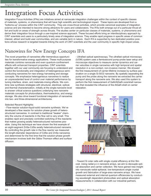
- Ultrafast optical spectroscopy. The ultrafast optical microscopy<br />
(UOM) system uses a femtosecond pump-probe laser setup and<br />
microscope objectives to measure carrier dynamics and carrier<br />
velocities in single nanowires with high temporal and spatial<br />
resolution in a non-contact, non-invasive manner. We showed<br />
the first measurement of carrier-lifetime increase by surface passivation<br />
on a single Si-SiO2 nanowire. By spatially separating the<br />
pump and the probe along the nanowire we extracted the carrier<br />
transport along the nanowire axis. We also used this system to<br />
per<strong>for</strong>m the first measurement of GaN/AlGaN core/shell nanowires<br />
that revealed the influence of the AlGaN shell on carrier<br />
relaxation.<br />
Selected Recent Highlights:<br />
- Flow-reactor solution-liquid-solid nanowire synthesis. We’ve<br />
developed a flow reactor <strong>for</strong> solution phase growth of heterostructured<br />
nanowires. In contrast to traditional “beaker” chemistry<br />
the volume of reactants in the flow cell is very small. This<br />
enables rapid and precisely controlled switching of the reactants<br />
that makes growing axially heterostructured nanowires possible.<br />
Using this technique we have shown the first example of<br />
an eight-segment ZnSe-CdSe axially heterostructured nanowire.<br />
By controlling the growth rate in the flow reactor we measured<br />
the length-diameter dependence of CdSe and ZnSe nanowires<br />
and determined <strong>for</strong> the first time that the solution-phase growth<br />
mechanism involves both the Gibbs-Thomson effect and surface<br />
diffusion.<br />
- Toward Si colar cells with single crystal efficiency at thin film<br />
cost. Using radial p-i-n nanowire arrays, we aim to decouple optical<br />
absorption and carrier collection. We have gained new insight<br />
into nanoscale radial epitaxial, low-temperature single crystal<br />
growth and fabrication of large-area nanowire arrays. We have<br />
measured external and internal quantum efficiencies by conducting<br />
wavelength dependent photovoltaic and optical absorption<br />
measurements in collaboration with our industrial partners.<br />
10<br />
10The <strong>Center</strong> <strong>for</strong> <strong>Integrated</strong> <strong>Nanotechnologies</strong> | <strong>2011</strong> <strong>Annual</strong> <strong>Report</strong>