2011 Annual Report - Center for Integrated Nanotechnologies - Los ...
2011 Annual Report - Center for Integrated Nanotechnologies - Los ...
2011 Annual Report - Center for Integrated Nanotechnologies - Los ...

Create successful ePaper yourself
Turn your PDF publications into a flip-book with our unique Google optimized e-Paper software.
Discovery Plat<strong>for</strong>ms<br />
Discovery Plat<strong>for</strong>ms <br />
The thrusts develop a variety of new instrumentation to advance<br />
the science in their areas. One ef<strong>for</strong>t unique to CINT is the Discovery<br />
Plat<strong>for</strong>m. These plat<strong>for</strong>ms are modular micro-laboratories<br />
designed and batch fabricated by CINT to allow easy integration<br />
of nanomaterials into microscale structures. Their purpose is<br />
to facilitate studies of nanomaterial properties and their integration.<br />
They should allow easy connections, a range of diagnostic<br />
and experimental measurement conditions, and a degree of<br />
standardization and reproducibility in nanoscale measurements.<br />
The inception, creation and evolution of Discovery Plat<strong>for</strong>ms have<br />
evolved in close collaboration with our user community.<br />
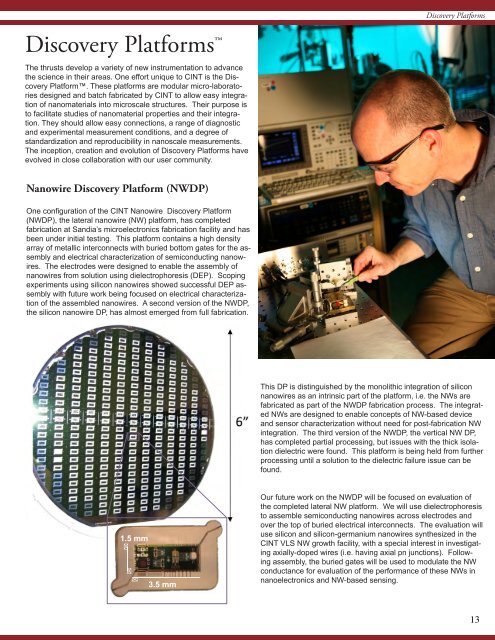
Nanowire Discovery Plat<strong>for</strong>m (NWDP)<br />
One configuration of the CINT Nanowire Discovery Plat<strong>for</strong>m<br />
(NWDP), the lateral nanowire (NW) plat<strong>for</strong>m, has completed<br />
fabrication at Sandia’s microelectronics fabrication facility and has<br />
been under initial testing. This plat<strong>for</strong>m contains a high density<br />
array of metallic interconnects with buried bottom gates <strong>for</strong> the assembly<br />
and electrical characterization of semiconducting nanowires.<br />
The electrodes were designed to enable the assembly of<br />
nanowires from solution using dielectrophoresis (DEP). Scoping<br />
experiments using silicon nanowires showed successful DEP assembly<br />
with future work being focused on electrical characterization<br />
of the assembled nanowires. A second version of the NWDP,<br />
the silicon nanowire DP, has almost emerged from full fabrication.<br />
This DP is distinguished by the monolithic integration of silicon<br />
nanowires as an intrinsic part of the plat<strong>for</strong>m, i.e. the NWs are<br />
fabricated as part of the NWDP fabrication process. The integrated<br />
NWs are designed to enable concepts of NW-based device<br />
and sensor characterization without need <strong>for</strong> post-fabrication NW<br />
integration. The third version of the NWDP, the vertical NW DP,<br />
has completed partial processing, but issues with the thick isolation<br />
dielectric were found. This plat<strong>for</strong>m is being held from further<br />
processing until a solution to the dielectric failure issue can be<br />
found.<br />
1.5 mm<br />
<br />
<br />
<br />
3.5 mm<br />
Our future work on the NWDP will be focused on evaluation of<br />
the completed lateral NW plat<strong>for</strong>m. We will use dielectrophoresis<br />
to assemble semiconducting nanowires across electrodes and<br />
over the top of buried electrical interconnects. The evaluation will<br />
use silicon and silicon-germanium nanowires synthesized in the<br />
CINT VLS NW growth facility, with a special interest in investigating<br />
axially-doped wires (i.e. having axial pn junctions). Following<br />
assembly, the buried gates will be used to modulate the NW<br />
conductance <strong>for</strong> evaluation of the per<strong>for</strong>mance of these NWs in<br />
nanoelectronics and NW-based sensing.<br />
13