2011 Annual Report - Center for Integrated Nanotechnologies - Los ...
2011 Annual Report - Center for Integrated Nanotechnologies - Los ...
2011 Annual Report - Center for Integrated Nanotechnologies - Los ...

You also want an ePaper? Increase the reach of your titles
YUMPU automatically turns print PDFs into web optimized ePapers that Google loves.
News from <strong>2011</strong><br />
News from <strong>2011</strong><br />
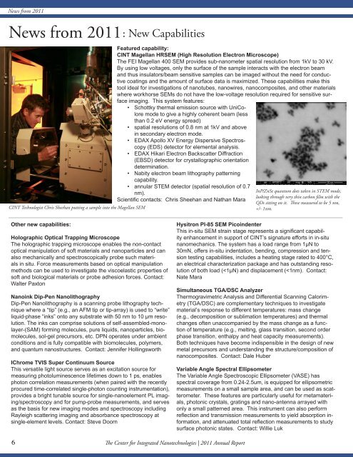
CINT Technologist Chris Sheehan putting a sample into the Magellan SEM<br />
: New Capabilities<br />
Featured capability:<br />
CINT Magellan HRSEM (High Resolution Electron Microscope)<br />
The FEI Magellan 400 SEM provides sub-nanometer spatial resolution from 1kV to 30 kV.<br />
By using low voltages, only the surface of the sample interacts with the electron beam<br />
and thus insulators/beam sensitive samples can be imaged without the need <strong>for</strong> conductive<br />
coatings and the amount of surface data is maximized. These capabilities make this<br />
tool ideal <strong>for</strong> investigations of nanotubes, nanowires, nanocomposites, and other materials<br />
where workhorse SEMs do not have the low-voltage resolution required <strong>for</strong> sensitive surface<br />
imaging. This system features:<br />
• Schottky thermal emission source with UniColore<br />
mode to give a highly coherent beam (less<br />
than 0.2 eV energy spread)<br />
• spatial resolutions of 0.8 nm at 1kV and above<br />
in secondary electron mode.<br />
• EDAX Apollo XV Energy Dispersive Spectroscopy<br />
(EDS) detector <strong>for</strong> elemental analysis.<br />
• EDAX Hikari Electron Backscatter Diffraction<br />
(EBSD) detector <strong>for</strong> crystallographic orientation<br />
determination.<br />
• Nabity electron beam lithography patterning<br />
capability.<br />
• annular STEM detector (spatial resolution of 0.7<br />
nm).<br />
Scientific contacts: Chris Sheehan and Nathan Mara<br />
InP/ZnSe quantum dots taken in STEM mode,<br />
looking through very thin carbon film with the<br />
QDs sitting on it. These measured to be 5 nm,<br />
+/- 1nm.<br />
Other new capabilities:<br />
Holographic Optical Trapping Microscope<br />
The holographic trapping microscope enables the non-contact<br />
optical manipulation of soft materials and nanoparticles and can<br />
also mechanically and spectroscopically probe such materials<br />
in situ. Force measurements based on optical manipulation<br />
methods can be used to investigate the viscoelastic properties of<br />
soft and biological materials or probe adhesion <strong>for</strong>ces. Contact:<br />
Walter Paxton<br />
Nanoink Dip-Pen Nanolithography<br />
Dip-Pen Nanolithography is a scanning probe lithography technique<br />
where a “tip” (e.g., an AFM tip or tip-array) is used to “write”<br />
liquid-phase “inks” onto any substrate with 50 nm to 10 μm resolution.<br />
The inks can comprise solutions of self-assembled-monolayer-(SAM)<br />
<strong>for</strong>ming molecules, pure liquids, nanoparticles, biomolecules,<br />
sol-gel precursors, etc. DPN operates under ambient<br />
conditions and is fully compatible with biomolecules, polymers,<br />
and quantum nanostructures. Contact: Jennifer Hollingsworth<br />
IChrome TVIS Super Continuum Source<br />
This versatile light source serves as an excitation source <strong>for</strong><br />
measuring photoluminescence lifetimes down to 1 ps, enables<br />
photon correlation measurements (when paired with the recently<br />
procured time-correlated single-photon counting instrumentation),<br />
provides a bright tunable source <strong>for</strong> single-nanoelement PL imaging/spectroscopy<br />
and <strong>for</strong> pump-probe measurements, and serves<br />
as the basis <strong>for</strong> new imaging modes and spectroscopy including<br />
Rayleigh scattering imaging and absorbance spectroscopy at<br />
single-element levels. Contact: Steve Doorn<br />
Hysitron PI-85 SEM Picoindenter<br />
This in-situ SEM strain stage represents a significant capability<br />
enhancement in support of CINT’s signature ef<strong>for</strong>ts in in-situ<br />
nanomechanics. The system has a load range from 1µN to<br />
30mN, offers in-situ indentation, bending, compression and tension<br />
testing capabilities, includes a heating stage rated to 400°C,<br />
an electrical characterization package and has outstanding resolution<br />
of both load (