2011 Annual Report - Center for Integrated Nanotechnologies - Los ...
2011 Annual Report - Center for Integrated Nanotechnologies - Los ...
2011 Annual Report - Center for Integrated Nanotechnologies - Los ...

Create successful ePaper yourself
Turn your PDF publications into a flip-book with our unique Google optimized e-Paper software.
Nanoscale Electronics & Mechanics Thrust<br />
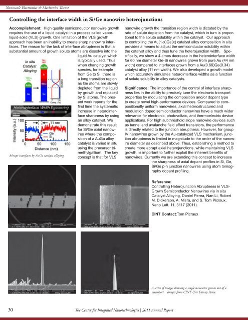
Controlling the interface width in Si/Ge nanowire heterojunctions<br />
Accomplishment: High quality semiconductor nanowire growth<br />
requires the use of a liquid catalyst in a process called vaporliquid-solid<br />
(VLS) growth. One limitation of the VLS growth<br />
approach has been an inability to create sharp nanowire interfaces.<br />
The reason <strong>for</strong> the lack of interface abruptness is that a<br />
substantial amount of growth solute atoms are dissolve into the<br />
liquid Au catalyst which<br />
is typically used. Thus<br />
when changing growth<br />
species, <strong>for</strong> example<br />
from Ge to Si, there is<br />
a long transition region<br />
as Ge atoms are slowly<br />
depleted from the liquid<br />
by growth and replaced<br />
by Si atoms. The present<br />
work reports <strong>for</strong> the<br />
first time the systematic<br />
increase in heterointerface<br />
sharpness by using<br />
an alloy catalyst. We<br />
demonstrate this result<br />
<strong>for</strong> Si/Ge axial nanowires<br />
where the composition<br />
of a AuGa alloy<br />
catalyst is varied in situ<br />
using the precursor trimethylgallium.<br />
The key<br />
Abrupt interfaces by AuGa catalyst alloying.<br />
concept is that <strong>for</strong> VLS<br />
nanowire growth the transition region width is dictated by the<br />
rate of solute depletion from the catalyst, which in turn is proportional<br />
to the solute solubility within the catalyst. Our approach<br />
to controlling the Au(1-x)Ga(x) catalyst alloy composition in situ<br />
provides a means to adjust the semiconductor solubility within<br />
the catalyst alloy and thus tune the heterojunction width. Specifically,<br />
we show a 4-times decrease in the heterointerface width<br />
<strong>for</strong> 60 nm diameter Ge-Si nanowires grown from pure Au (44 nm<br />
width) compared to interfaces grown from a Au(0.66)Ga(0.34)<br />
catalyst alloy (11 nm width). We also developed a growth model<br />
which accurately simulates heterointerface widths as a function<br />
of solute solubility in alloy catalysts.<br />
Significance: The importance of the control of interface sharpness<br />
lies in the ability to precisely tune the electronic transport<br />
properties by modulating the composition and/or dopant type<br />
to create novel high-per<strong>for</strong>mance devices. Compared to compositionally<br />
uni<strong>for</strong>m nanowires, axial heterostructured and<br />
modulation doped semiconductor nanowires have a much wider<br />
relevance <strong>for</strong> electronic, photovoltaic, and thermoelectric device<br />
applications. For high subthreshold slope nanowire devices such<br />
as tunnel and avalanche field effect transistors, the per<strong>for</strong>mance<br />
is directly related to the junction abruptness. However, <strong>for</strong> group<br />
IV nanowires grown by the Au-catalyzed VLS mechanism, junction<br />
abruptness is limited in magnitude to the order of the nanowire<br />
diameter as described above. Thus, establishing a method to<br />
create more abrupt axial heterojunctions, while maintaining VLS<br />
growth, is important to further exploit the inherent benefits of<br />
nanowires. Currently we are extending this concept to increase<br />
the sharpness of axial dopant profiles in Si, Ge,<br />
Si/Ge p-n junction nanowires using atom tomography<br />
dopant profiling.<br />
Reference:<br />
Controlling Heterojunction Abruptness in VLS-<br />
Grown Semiconductor Nanowires via in situ<br />
Catalyst Alloying, Daniel Perea, Nan Li, Robert<br />
M. Dickerson, A. Misra, and S. Tom Picraux,<br />
Nano Lett. 11, 3117 (<strong>2011</strong>).<br />
CINT Contact:Tom Picraux<br />
A series of images showing a single nanowire grown out of a<br />
micropost. Images from CINT User Danny Perea.<br />
30<br />
30The <strong>Center</strong> <strong>for</strong> <strong>Integrated</strong> <strong>Nanotechnologies</strong> | <strong>2011</strong> <strong>Annual</strong> <strong>Report</strong>