FTGPIO010 - Faraday Technology Corporation
FTGPIO010 - Faraday Technology Corporation
FTGPIO010 - Faraday Technology Corporation

You also want an ePaper? Increase the reach of your titles
YUMPU automatically turns print PDFs into web optimized ePapers that Google loves.
<strong>FTGPIO010</strong><br />
GENERAL PURPOSE INPUT / OUTPUT<br />
Version 1.4 | October 2006<br />
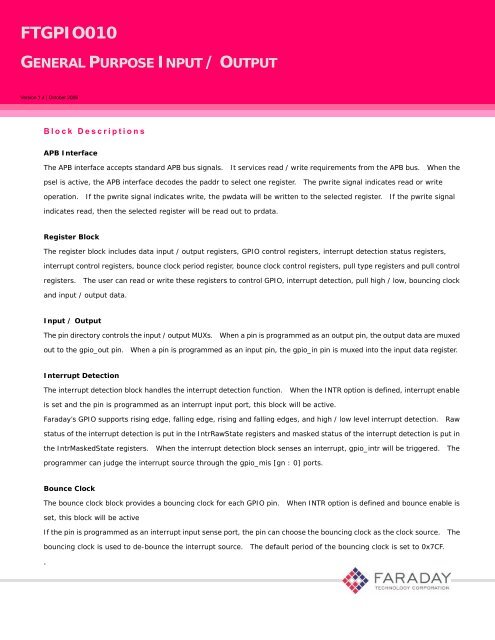
Block Descriptions<br />
APB Interface<br />
The APB interface accepts standard APB bus signals. It services read / write requirements from the APB bus. When the<br />
psel is active, the APB interface decodes the paddr to select one register. The pwrite signal indicates read or write<br />
operation. If the pwrite signal indicates write, the pwdata will be written to the selected register. If the pwrite signal<br />
indicates read, then the selected register will be read out to prdata.<br />
Register Block<br />
The register block includes data input / output registers, GPIO control registers, interrupt detection status registers,<br />
interrupt control registers, bounce clock period register, bounce clock control registers, pull type registers and pull control<br />
registers. The user can read or write these registers to control GPIO, interrupt detection, pull high / low, bouncing clock<br />
and input / output data.<br />
Input / Output<br />
The pin directory controls the input / output MUXs. When a pin is programmed as an output pin, the output data are muxed<br />
out to the gpio_out pin. When a pin is programmed as an input pin, the gpio_in pin is muxed into the input data register.<br />
Interrupt Detection<br />
The interrupt detection block handles the interrupt detection function. When the INTR option is defined, interrupt enable<br />
is set and the pin is programmed as an interrupt input port, this block will be active.<br />
<strong>Faraday</strong>’s GPIO supports rising edge, falling edge, rising and falling edges, and high / low level interrupt detection. Raw<br />
status of the interrupt detection is put in the IntrRawState registers and masked status of the interrupt detection is put in<br />
the IntrMaskedState registers. When the interrupt detection block senses an interrupt, gpio_intr will be triggered. The<br />
programmer can judge the interrupt source through the gpio_mis [gn : 0] ports.<br />
Bounce Clock<br />
The bounce clock block provides a bouncing clock for each GPIO pin. When INTR option is defined and bounce enable is<br />
set, this block will be active<br />
If the pin is programmed as an interrupt input sense port, the pin can choose the bouncing clock as the clock source. The<br />
bouncing clock is used to de-bounce the interrupt source. The default period of the bouncing clock is set to 0x7CF.<br />
.