Faraday ARM Common Platform - Faraday Technology Corporation
Faraday ARM Common Platform - Faraday Technology Corporation
Faraday ARM Common Platform - Faraday Technology Corporation

You also want an ePaper? Increase the reach of your titles
YUMPU automatically turns print PDFs into web optimized ePapers that Google loves.
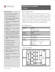
DDR Memory Controller<br />
<strong>Faraday</strong> / UMC FTDDRII020_S<br />
Key Features<br />
General Description<br />
• AHB 2.0 compliant <strong>Faraday</strong>’s DDRII memory controller (FTDDRII020_S) is an AMBA AHB 2.0 compliant Double<br />
• Rich DDRII RAM type support, up to 2G bytes<br />
• Use burst length of 4 to speed up the read /write<br />
cycle<br />
• Programmable refresh type (Staggered or<br />
Non-Staggered)<br />
• Support DDRII RAM address phase 1T or 2T<br />
(2T is for heavy loading)<br />
• Support two AHB buses, i.e. controller has two<br />
AHB channels<br />
• Support 1 DIMM, 2 RANKs (2 chip selects)<br />
• Support DDRII Power-down, DDRII RAM will<br />
enter self-refresh mode<br />
• Prefetch the Sequential Read Data for AHB<br />
Burst Read command<br />
• Separate memory controller into a four-stage<br />
pipeline to support high frequency clock<br />
(HCLK)<br />
• Support Post CAS (AL = 2) when tRCD >= 4T<br />
• Connect with three <strong>Faraday</strong> DDRII Hard Cores:<br />
a. DDRDATA16BIT<br />
b. DDRCMDADDR<br />
c. COMPBLK<br />
• Need 1x (266 MHz) and 2x (533 MHz) clock<br />
inputs which must be rising edge locked<br />
Data Rate RAM controller which supports rich types of DDRII RAM. The controller uses a<br />
DDRII burst length of 4 to accelerate the read / write speed. It separates the design into a<br />
four-stage pipeline to support high frequency. It can also prefetch the AHB master’s sequential<br />
read data for AHB burst read command.<br />
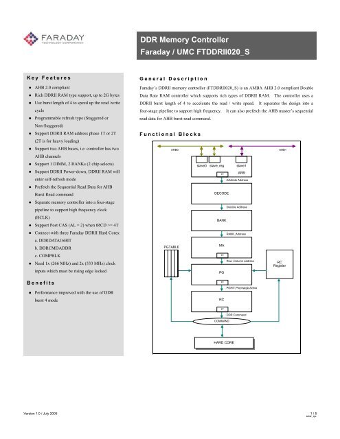
Functional Blocks<br />
AHB0<br />
PGTABLE<br />
slave0 slave_reg slave1<br />
FF<br />
DECODE<br />
BANK<br />
MA<br />
FF<br />
PG<br />
ARB<br />
Arbitrate Address<br />
Decode Address<br />
RANK_Address<br />
Row ,Column address<br />
AHB1<br />
RC<br />
Register<br />
Benefits<br />
• Performance improved with the use of DDR<br />
burst 4 mode<br />
FF<br />
RC<br />
PGHIT,Precharge,Active<br />
FF<br />
DDR Command<br />
COMMAND<br />
HARD CORE<br />
Version 1.0 / July 2005 1 / 5<br />
KMC_QA
FTDDRII020S<br />
http://www.faraday-tech.com<br />
Block Descriptions<br />
The DDRII memory controller separates the design into 4 stages of function block, including ARB, DECODE-BANK-MA, PG, and RC stages, ended with the<br />
CMD block. The following is a detailed description of each building block.<br />
• ARB stage<br />
This stage comprises two AHB memory slaves (slave 0 and slave 1) and one AHB register slave (slave_reg). The AHB memory slave performs the normal<br />
read and write function, while the AHB register slave allows AHB master to read/write the DDRII controller registers. This stage has read/write command<br />
queue, and read/write data queue. This stage arbitrates the read/write command queue requests, and selects the highest priority request, then pipes this<br />
request’s address to the DEC-BANK-MA stage.<br />
• DEC-BANK-MA stage<br />
This stage decodes the Address, if it is a burst read request, and generates the next Address for prefetching the next read data. If it is a write request, this<br />
stage will get the Address from the write command queue after decoding the Address, and then go to the BANK block.<br />
This BANK block will calculate the Address mapping to the chip-select (RANK), and at the same time, the Address will subtract 2 ranks from the top<br />
Address, which Address is the DDRII DIMM real Address, then goes to MA block.<br />
MA block contains an MA-table for DDRII controller to support rich types of DDRII RAM. Different types of DDRII RAM may have different column or<br />
row Addresses, so we need to generate the column, bank, row, Address for each RANK, before piping to PG stage.<br />
• PG stage<br />
The page stage contains a page table which memorizes which page of the bank is open, that is, we can open 4 rows at a time. Besides, this stage will<br />
compare the column, row Address, decide whether the Address is page miss or hit, and whether it needs active or precharge command or both. This page<br />
table will be changed by the command stage, for example, active and precharge commands. Then the needed command is piped to RC stage.<br />
• RC stage<br />
This stage will consider the RC timing, like read to read, read to write, precharge to read and so on, then generate the pre_command, which will not<br />
violate the DDRII spec. The RC counter is located in the RC register block. If RC check is passed, then the actual DDRII command is sent. This stage is<br />
the final stage before the actual DDRII command.<br />
• CMD Block<br />
This block is the actual DDRII command output block, which only outputs the RC stage’s pre_command. This stage also has a state machine to control the<br />
refresh command, with its state machine center controlling the pipeline.<br />
2 / 5 Version 1.0 / July 2005<br />
KMC_QA
http://www.faraday-tech.com<br />
FTDDRII020S<br />
Signal Connection<br />
DDRCMDADDRALL<br />
AHB0<br />
DDRDATA16BIT<br />
DDR2 Controller<br />
DDR2 RAM<br />
DDRDATA16BIT<br />
AHB1<br />
COMPBLK<br />
Signal Definition<br />
AHB interface<br />
Signal Name I/O Description (n=0 or 1)<br />
HCLK I System bus clock<br />
rst_n I Active low system reset<br />
hready_inn I System bus ready inputs<br />
reg_hsel I AHB slave select for AHB slave (reg.)<br />
hseln I AHB slave select for AHB slave n<br />
HADDRn[31:0] I AHB Address for AHB slave n<br />
hwriten I AHB write indicator for AHB slaven<br />
htransn[2:0] I AHB transfer type for AHB slaven<br />
hsizen[2:0] I AHB size indicators for AHB slaven<br />
hburstn[2:0] I AHB burst indicators for AHB slaven<br />
hwdatan[31:0] I AHB write data bus for AHB slaven<br />
hready_out_reg O Slave ready from AHB slave (reg.) to AHB0<br />
hready_outn O Slave ready from slave n to AHB n<br />
Hresp_reg[1:0] O Slave response from AHB slave (reg.) to AHB0<br />
hrespn[1:0] O Slave response from AHB slave n to AHB n<br />
hrdata_reg[31:0] O Slave read data bus from AHB slave (reg.) to AHB0<br />
hrdatan[31:0] O Slave read data bus from AHB slave n to AHB n<br />
ddr_sref_ack O Not used<br />
ddr_sref_req I Must be assigned 1’b0, not used<br />
ddr_hclkx2 I DDRII needs 1x and 2x clock inputs that are rising edge locked<br />
push_rdq O Not used<br />
Version 1.0 / July 2005 3 / 5<br />
KMC_QA
FTDDRII020S<br />
http://www.faraday-tech.com<br />
HardCore DDRCMDADDRALL [DDR RAM] interface<br />
Signal Name I/O Description<br />
ddr_csn[1:0] O Active low ddr chip-enable<br />
ddr_rasn O Active-low row Address strobe indicator<br />
ddr_casn O Active-low column Address strobe indicator<br />
ddr_wen O Active-low write enable indicator for ddr modules<br />
ddr_addr [13:0] O Address bus for ddr modules<br />
ddr_ba [2:0] O ddr bank Address bus for ddr modules<br />
ddr_dqm [3:0] O ddr data mask for ddr modules<br />
ddr_cke O ddr clock enable control signal<br />
ODT[1:0] O On Die Termination control signal<br />
ODT_en O Enable the HardCore’s On Die Termination<br />
HardCore DDRDATA16BIT interface-1<br />
Signal Name I/O Description<br />
Odtmd[1:0] O Connect to DDRDATA16BIT<br />
Dllselhb[7:2] O Connect to DDRDATA16BIT<br />
Dllsellb[13:8] O Connect to DDRDATA16BIT<br />
Wrdllsel[19:14] O Connect to DDRDATA16BIT<br />
Bypassen O Connect to DDRDATA16BIT<br />
Lbpwten O Connect to DDRDATA16BIT<br />
Dqsbypass O Connect to DDRDATA16BIT<br />
Sio O Connect to DDRDATA16BIT<br />
HardCore DDRDATA16BIT interface-2<br />
Signal Names I/O Description<br />
DQTESTO[15:0] I Connect to DDRDATA16BIT<br />
HDMDQTESTO I Connect to DDRDATA16BIT<br />
HDQSTESTO I Connect to DDRDATA16BIT<br />
LDMDQTESTO, I Connect to DDRDATA16BIT<br />
LDQSTESTO I Connect to DDRDATA16BIT<br />
FLDO_data I Connect to DDRDATA16BIT<br />
rdqodd I Connect to DDRDATA16BIT<br />
rdqeven I Connect to DDRDATA16BIT<br />
dqs_oe O Connect to DDRDATA16BIT<br />
dqoe O Connect to DDRDATA16BIT<br />
dataeven O Connect to DDRDATA16BIT<br />
dataodd O Connect to DDRDATA16BIT<br />
EVEN_DQM O Connect to DDRDATA16BIT<br />
ODD_DQM O Connect to DDRDATA16BIT<br />
clkwrptr O Connect to DDRDATA16BIT<br />
Rdcnt O Connect to DDRDATA16BIT<br />
4 / 5 Version 1.0 / July 2005<br />
KMC_QA
http://www.faraday-tech.com<br />
FTDDRII020S<br />
HardCore DDRCMDADDRALL interface-1<br />
Signal Name I/O Description<br />
WRDLLCMD[5:0] O Connect to DDRCMDADDRALL<br />
WRDLLCLK[11:6] O Connect to DDRCMDADDRALL<br />
Wten O Connect to DDRCMDADDRALL<br />
ADDRTESTO O Connect to DDRCMDADDRALL<br />
BATESTO O Connect to DDRCMDADDRALL<br />
CASTESTO O Connect to DDRCMDADDRALL<br />
CKETESTO O Connect to DDRCMDADDRALL<br />
CKTESTO0 O Connect to DDRCMDADDRALL<br />
CKTESTO1 O Connect to DDRCMDADDRALL<br />
CKTESTO2 O Connect to DDRCMDADDRALL<br />
CSTESTO O Connect to DDRCMDADDRALL<br />
FLDO_addr O Connect to DDRCMDADDRALL<br />
ODTTESTO O Connect to DDRCMDADDRALL<br />
RASTESTO O Connect to DDRCMDADDRALL<br />
WETESTO O Connect to DDRCMDADDRALL<br />
HardCore COMPBLK<br />
Signal Name I/O Description<br />
COMP_SEL O Connect to COMPBLK<br />
DOP<br />
Reserved<br />
DON<br />
Reserved<br />
DIP<br />
Reserved<br />
DIN<br />
Reserved<br />
En_COMPBLK O Connect to COMPBLK<br />
HardCore Other Connect<br />
Signal Names I/O Description<br />
TestDCInput ; O Reserved<br />
Boundary_Testen O Connect to all Hard Blocks<br />
Bscanmode O Connect to all Hard Blocks<br />
HEADQUARTERS USA OFFICE EUROPE OFFICE<br />
JAPAN OFFICE CHINA OFFICE<br />
Hsinchu, Taiwan<br />
Sunnyvale, USA Hoofddorp, Netherlands Tokyo, Japan Shanghai, P. R. China<br />
Tel: 886-3-578-7888 Tel: 1-408-522-8888 Tel: 31-2356-20496 Tel: 81-3-5214-0070 Tel: 86-21-6406-7523<br />
Fax: 886-3-578-7889 Fax: 1-408-522-8889 Fax: 31-2356-36297 Fax: 81-3-5214-0076 Fax: 86-21-6406-5327<br />
twsales@faraday-tech.com ussales@faraday-tech.com eusales@faraday-tech.com jpsales@faraday-tech.com cnsales@faraday-tech.com<br />
Copyright <strong>Faraday</strong> <strong>Technology</strong>, 2005. All Rights Reserved. <strong>Faraday</strong> and <strong>Faraday</strong> Logo are trademarks of <strong>Faraday</strong> <strong>Technology</strong> <strong>Corporation</strong>. Nothing in this document<br />
shall operate as license or is with express or implied warranty. The <strong>Faraday</strong> home page can be found at www.faraday-tech.com<br />
Version 1.0 / July 2005 5 / 5<br />
KMC_QA