Faraday ARM Common Platform - Faraday Technology Corporation
Faraday ARM Common Platform - Faraday Technology Corporation
Faraday ARM Common Platform - Faraday Technology Corporation

You also want an ePaper? Increase the reach of your titles
YUMPU automatically turns print PDFs into web optimized ePapers that Google loves.
FTDDRII020S<br />
http://www.faraday-tech.com<br />
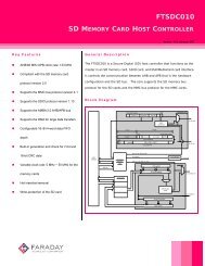
Block Descriptions<br />
The DDRII memory controller separates the design into 4 stages of function block, including ARB, DECODE-BANK-MA, PG, and RC stages, ended with the<br />
CMD block. The following is a detailed description of each building block.<br />
• ARB stage<br />
This stage comprises two AHB memory slaves (slave 0 and slave 1) and one AHB register slave (slave_reg). The AHB memory slave performs the normal<br />
read and write function, while the AHB register slave allows AHB master to read/write the DDRII controller registers. This stage has read/write command<br />
queue, and read/write data queue. This stage arbitrates the read/write command queue requests, and selects the highest priority request, then pipes this<br />
request’s address to the DEC-BANK-MA stage.<br />
• DEC-BANK-MA stage<br />
This stage decodes the Address, if it is a burst read request, and generates the next Address for prefetching the next read data. If it is a write request, this<br />
stage will get the Address from the write command queue after decoding the Address, and then go to the BANK block.<br />
This BANK block will calculate the Address mapping to the chip-select (RANK), and at the same time, the Address will subtract 2 ranks from the top<br />
Address, which Address is the DDRII DIMM real Address, then goes to MA block.<br />
MA block contains an MA-table for DDRII controller to support rich types of DDRII RAM. Different types of DDRII RAM may have different column or<br />
row Addresses, so we need to generate the column, bank, row, Address for each RANK, before piping to PG stage.<br />
• PG stage<br />
The page stage contains a page table which memorizes which page of the bank is open, that is, we can open 4 rows at a time. Besides, this stage will<br />
compare the column, row Address, decide whether the Address is page miss or hit, and whether it needs active or precharge command or both. This page<br />
table will be changed by the command stage, for example, active and precharge commands. Then the needed command is piped to RC stage.<br />
• RC stage<br />
This stage will consider the RC timing, like read to read, read to write, precharge to read and so on, then generate the pre_command, which will not<br />
violate the DDRII spec. The RC counter is located in the RC register block. If RC check is passed, then the actual DDRII command is sent. This stage is<br />
the final stage before the actual DDRII command.<br />
• CMD Block<br />
This block is the actual DDRII command output block, which only outputs the RC stage’s pre_command. This stage also has a state machine to control the<br />
refresh command, with its state machine center controlling the pipeline.<br />
2 / 5 Version 1.0 / July 2005<br />
KMC_QA