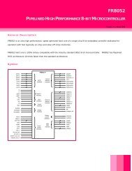
FTGPIO010 - Faraday Technology Corporation
FTGPIO010 - Faraday Technology Corporation
FTGPIO010 - Faraday Technology Corporation

You also want an ePaper? Increase the reach of your titles
YUMPU automatically turns print PDFs into web optimized ePapers that Google loves.
<strong>FTGPIO010</strong><br />
GENERAL PURPOSE INPUT / OUTPUT<br />
Version 1.4 | October 2006<br />
Key Features<br />
General Description<br />
• Speed: 66 MHz APB clock rate<br />
• Compliant with AMBA Specification Rev 2.0<br />
• Up to 32 independent input, output and<br />
output enable buses for bi-directional I/O<br />
pins<br />
• Each port can be programmed as a bypass<br />
pin<br />
• Each port can separately trigger GPIO<br />
interrupt when INTR option is set and<br />
programmed as an input pin<br />
• Each port interrupt generation can be<br />
triggered by rising edge, falling edge, rising<br />
and falling edges, and high / low levels<br />
when INTR option is set<br />
<strong>Faraday</strong>’s General Purpose Input / Output (<strong>FTGPIO010</strong>) is a flexible,<br />
configurable and programmable general-purpose I/O controller. It provides<br />
INTR and PULL options to remove or add the interrupt sense, bouncing clock,<br />
and pull high/low circuits. Each GPIO pin's attributes, like input/output,<br />
bypass, interrupt sense, clock source and pull type can be programmed to fit<br />
user specification.<br />
When programmed to be an interrupt input controller, the GPIO supports<br />
rising edge, falling edge, rising and falling edges, and high/low level interrupt<br />
sense types. The interrupt sense type varies with different device<br />
requirements. The GPIO also provides a bouncing clock for de-bounce input<br />
usage. The bounce period can be set to fit different requirements. Each pin<br />
can be programmed to choose bus clock or bouncing clock. <strong>Faraday</strong>’s GPIO<br />
provides up to 32 programmable I/O ports and each port can be<br />
independently programmed.<br />
• Each port can be pulled high or pulled low<br />
when PULL option is set (I/O pad<br />
programming required)<br />
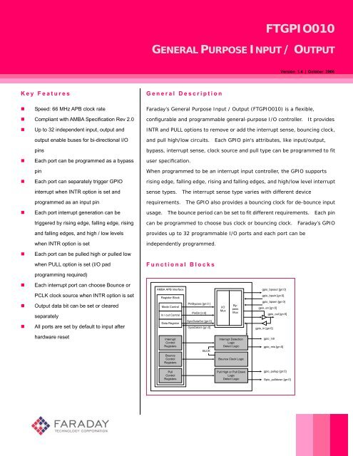
Functional Blocks<br />
• Each interrupt port can choose Bounce or<br />
PCLK clock source when INTR option is set<br />
• Output data bit can be set or cleared<br />
separately<br />
• All ports are set by default to input after<br />
AMBA APB Interface<br />
Register Block<br />
Mode Control<br />
In / out Control<br />
Data Register<br />
PinBypass [gn:0 ]<br />
PinDir [n:0]<br />
GpioDataOut [gn:0]<br />
GpioDataIn [gn:0]<br />
I/O<br />
Mux<br />
Bypass<br />
Mux<br />
gpio_bpsout [gn:0]<br />
gpio_bpsin [gn:0]<br />
gpio_bpsen [gn:0]<br />
gpio_en [gn:0]<br />
gpio_out [gn:0]<br />
gpio_in [gn:0]<br />
hardware reset<br />
Interrupt<br />
Control<br />
Registers<br />
Bounce<br />
Control<br />
Registers<br />
BLCK<br />
Interrupt Detection<br />
Logic<br />
Detect Logic<br />
Bounce Clock Logic<br />
gpio_intr<br />
gpio_mis [gn:0]<br />
Pull<br />
Control<br />
Registers<br />
Pull High or Pull Down<br />
Logic<br />
Detect Logic<br />
gpio_pullup [gn:0]<br />
Gpio_pulldown [gn:0]
<strong>FTGPIO010</strong><br />
GENERAL PURPOSE INPUT / OUTPUT<br />
Version 1.4 | October 2006<br />
Block Descriptions<br />
APB Interface<br />
The APB interface accepts standard APB bus signals. It services read / write requirements from the APB bus. When the<br />
psel is active, the APB interface decodes the paddr to select one register. The pwrite signal indicates read or write<br />
operation. If the pwrite signal indicates write, the pwdata will be written to the selected register. If the pwrite signal<br />
indicates read, then the selected register will be read out to prdata.<br />
Register Block<br />
The register block includes data input / output registers, GPIO control registers, interrupt detection status registers,<br />
interrupt control registers, bounce clock period register, bounce clock control registers, pull type registers and pull control<br />
registers. The user can read or write these registers to control GPIO, interrupt detection, pull high / low, bouncing clock<br />
and input / output data.<br />
Input / Output<br />
The pin directory controls the input / output MUXs. When a pin is programmed as an output pin, the output data are muxed<br />
out to the gpio_out pin. When a pin is programmed as an input pin, the gpio_in pin is muxed into the input data register.<br />
Interrupt Detection<br />
The interrupt detection block handles the interrupt detection function. When the INTR option is defined, interrupt enable<br />
is set and the pin is programmed as an interrupt input port, this block will be active.<br />
<strong>Faraday</strong>’s GPIO supports rising edge, falling edge, rising and falling edges, and high / low level interrupt detection. Raw<br />
status of the interrupt detection is put in the IntrRawState registers and masked status of the interrupt detection is put in<br />
the IntrMaskedState registers. When the interrupt detection block senses an interrupt, gpio_intr will be triggered. The<br />
programmer can judge the interrupt source through the gpio_mis [gn : 0] ports.<br />
Bounce Clock<br />
The bounce clock block provides a bouncing clock for each GPIO pin. When INTR option is defined and bounce enable is<br />
set, this block will be active<br />
If the pin is programmed as an interrupt input sense port, the pin can choose the bouncing clock as the clock source. The<br />
bouncing clock is used to de-bounce the interrupt source. The default period of the bouncing clock is set to 0x7CF.<br />
.
<strong>FTGPIO010</strong><br />
GENERAL PURPOSE INPUT / OUTPUT<br />
Version 1.4 | October 2006<br />
Pull High / Low<br />
The pull high / low block can pull the pad high or low. When PULL option is defined and pull enable is set, this block will<br />
be active.<br />
This function requires programming of the I/O pad.<br />
Bypass Architecture Diagram<br />
PinDir [0]<br />
0<br />
1<br />
GpioDataOut [0]<br />
0<br />
PAD [0]<br />
1<br />
PRDATA [0]<br />
GpioDataIn [0]<br />
gpio_bpsen [0]<br />
gpio_bpsin [0]<br />
gpio_bpsout [0]<br />
PinBypass [0]<br />
To support the bypass mode, two MUXs and one AND gate should be added. The PinBypass register controls the bypass<br />
mode. If PinBypass [0] is set, it means that pin [0] is in bypass mode and all PAD [0] inputs / outputs are controlled by<br />
gpio_bpsin [0], gpio_bpsen [0] and gpio_bpsout [0]. Please refer to the above figure. When the PinBypass [0] register<br />
is set, gpio_bpsen [0] will be muxed to PAD [0] output enable, which means that gpio_bpsen [0] can determine the pin<br />
direction directly. Similarly, in bypass mode, gpio_bpsin [0] is directly muxed to the PAD [0] output and the PAD [0] input<br />
is directly connected to gpio_bpsout [0].
<strong>FTGPIO010</strong><br />
GENERAL PURPOSE INPUT / OUTPUT<br />
Version 1.4 | October 2006<br />
Signal Descriptions<br />
gpio_bpsout [gn:0]<br />
PCLK<br />
PRSTn<br />
psel<br />
penable<br />
pwrite<br />
paddr [6:2]<br />
pwdata [gn:0]<br />
prdata [gn:0]<br />
GPIO<br />
Module<br />
gpio_bpsin [gn:0]<br />
gpio_bpsen [gn:0]<br />
gpin_en [gn:0]<br />
gpio_out [gn:0]<br />
gpio_in [gn:0]<br />
gpio_pullup [gn:0]<br />
gpio_pulldown [gn:0]<br />
gpio_intr<br />
gpio_mis [gn:0]<br />
AMBA APB Signal Descriptions<br />
Signal Name Direction Description<br />
PCLK I AMBA APB clock, used to time all bus transfers<br />
PRSTn I AMBA APB reset signal, active LOW<br />
psel I GPIO select signal from the APB bus. When set to 1, this signal indicates that the slave<br />
device is selected by the AMBA APB bridge, and that a data transfer is required.<br />
penable I AMBA APB enable signal<br />
pwrite I AMBA APB transfer direction signal. It indicates a write access when HIGH, and a read<br />
access when LOW.<br />
paddr I AMBA APB address bus<br />
pwdata I AMBA APB write data bus<br />
prdata O AMBA APB read data bus
<strong>FTGPIO010</strong><br />
GENERAL PURPOSE INPUT / OUTPUT<br />
Version 1.4 | October 2006<br />
<strong>FTGPIO010</strong> Signal Descriptions<br />
Signal Name Direction Description<br />
gpio_in I GPIO data input pin<br />
gpio_out O GPIO data output pin<br />
gpio_en O GPIO data output enable pin, active HIGH<br />
gpio_pullup O GPIO output pad pullup<br />
gpio_pulldown O GPIO output pad pulldown<br />
gpio_intr O GPIO interrupt. When high, this signal indicates that a valid match has occurred between<br />
any of the interrupts.<br />
gpio_mis O GPIO masked interrupt status. A high of the lines indicates that a valid match has<br />
occurred between the interrupt set of registers and the signals on the corresponding pads.<br />
gpio_bpsin I GPIO bypass input. Data bypass input signal, which controls pad output data and APB<br />
read data.<br />
gpio_bpsen I GPIO bypass enable. Data bypass output enable signal, which controls pad direction<br />
when PinBypass is set.<br />
gpio_bpsout O GPIO bypass output. Data bypass output signal, which passes data from gpio_bpsin<br />
when PinBypass is set.
HEADQUARTERS<br />
Hsinchu, Taiwan,<br />
Tel: 886-3-578-7888<br />
Fax: 886-3-578-7889<br />
twsales@faraday-tech.com<br />
USA OFFICE<br />
Sunnyvale, USA<br />
Tel: 1-408-522-8888<br />
Fax: 1-408-522-8889<br />
ussales@faraday-tech.com<br />
EUROPE OFFICE<br />
Hoofddorp, Netherlands<br />
Tel: 31-2356-20496<br />
Fax: 31-2356-36297<br />
eusales@faraday-tech.com<br />
JAPAN OFFICE<br />
Tokyo, Japan<br />
Tel: 81-3-5214-0070<br />
Fax: 81-3-5214-0076<br />
jpsales@faraday-tech.com<br />
CHINA OFFICE<br />
Shanghai, P. R. China<br />
Tel: 86-21-6406-7523<br />
Fax: 86-21-6406-5327<br />
cnsales@faraday-tech.com<br />
Copyright <strong>Faraday</strong> <strong>Technology</strong>, 2006. All Rights Reserved. <strong>Faraday</strong> and <strong>Faraday</strong> Logo are trademarks of <strong>Faraday</strong><br />
<strong>Technology</strong> <strong>Corporation</strong>. Nothing in this document shall operate as license or is with express or implied warranty.<br />
The <strong>Faraday</strong> home page can be found at www.faraday-tech.com