Fractional N synthesizers - Mobile Dev & Design
Fractional N synthesizers - Mobile Dev & Design
Fractional N synthesizers - Mobile Dev & Design

You also want an ePaper? Increase the reach of your titles
YUMPU automatically turns print PDFs into web optimized ePapers that Google loves.
signal processing<br />
<strong>Fractional</strong> N <strong>synthesizers</strong><br />
Analyzing fractional N <strong>synthesizers</strong> and their ability to reduce phase noise,<br />
improve loop speed and reduce reference spur levels.<br />
By Gary Appel<br />
The fractional N synthesizer has<br />
been credited with the ability to<br />
decrease phase noise, provide increased<br />
loop speed for a given step size, and<br />
provide reduced reference spur levels.<br />
This article will examine the waveforms<br />
produced by charge pumps when<br />
operating in the fractional N mode. It<br />
will use these waveforms to<br />
calculate approximate levels<br />
for the spurious sidebands<br />
created by the fractional N<br />
technique. While this article<br />
will not derive the loop equations<br />
for a phase-locked loop,<br />
it will go through some of the<br />
calculations required to get a<br />
simple loop up and running.<br />
Finally, it will examine<br />
the multiple-modulus<br />
divider provided in the chips<br />
and develop a concise algorithm<br />
for determining a<br />
valid set of divider numbers<br />
for the three- and four-modulus<br />
prescalers. While this<br />
analysis uses Phillips<br />
devices for presentation, the<br />
developed theory can be<br />
applied to all fractional N<br />
<strong>synthesizers</strong>.<br />
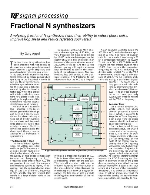
The fractional N loop<br />
In the traditional synthesizer,<br />
the voltage-controlled<br />
oscillator (VCO) frequency is<br />
at some integer multiple of<br />
the divided down reference<br />
frequency at the phase comparator<br />
(comparison frequency, or f comp ).<br />
Frequency steps smaller than f comp are<br />
not possible. As a result, the comparison<br />
frequency can be no higher, in frequency,<br />
than the desired channel spacing,<br />
or step size. If the VCO frequency<br />
is high, and the step size is small, this<br />
results in a large division ratio in the<br />
VCO path.<br />
A typical block diagram of a fractional N synthesizer (courtesy of Phillips).<br />
For example, with a 500 MHz VCO,<br />
and a channel spacing of 50 kHz, the<br />
VCO frequency will have to be divided<br />
by 10,000 to obtain the comparison frequency<br />
of 50 kHz. This will result in an<br />
increase of the phase detector noise of<br />
20 log 10000, or 80 dB. And the 50 kHz<br />
channel spacing will require a narrow<br />
loop bandwidth, to control the amplitude<br />
of the reference spurs. The narrowband<br />
loop will exhibit a slow transient<br />
response. The fractional N loop<br />
allows us to lock the VCO to a frequency<br />
that is a fractional multiple of f comp .<br />
This, in turn, allows use of a comparison<br />
frequency larger than the step size.<br />
The overall division ratio can be<br />
reduced, lowering the contribution of<br />
the phase detector noise. Because the<br />
reference spurs are now at a higher frequency,<br />
the loop can be sped up while<br />
retaining the same rejection of the reference<br />
spurs.<br />
As an example, consider again the<br />
500 MHz VCO, with the channel spacing<br />
of 50 kHz. The required division<br />
ratio for the standard loop, using a 50<br />
kHz comparison frequency, is 10,000.<br />
To set the VCO to 500.05 MHz would<br />
require the next integer division ratio,<br />
10,001. Now, increase the comparison<br />
frequency to 100 kHz, reducing the<br />
division ratio to 5,000. To set the VCO<br />
to 500.05 MHz would require a division<br />
ratio of 5000.5. The 0.5 is clearly unobtainable<br />
using a standard digital<br />
counter. The fractional N<br />
loop gets around this problem<br />
by alternating the division<br />
ratio between 5,000 and<br />
5,001. The average division<br />
ratio is then precisely<br />
5,000.5, just what we need to<br />
set the VCO on frequency.<br />
A closer look<br />
In a normal synthesizer,<br />
while locked, the phase<br />
detector produces a narrow<br />
pulse, which is required to<br />
keep the VCO on frequency.<br />
Each pulse from the phase<br />
detector should be identical<br />
to all the other pulses.<br />
In the fractional N loop<br />
described above, the VCO is<br />
never quite on frequency.<br />
That is, it is never an exact<br />
integer multiple of the comparison<br />
frequency. In one<br />
cycle of the comparison frequency<br />
the VCO frequency<br />
will appear to be high by half<br />
the comparison frequency. In<br />
the next cycle, the VCO will<br />
appear to be low by an equal<br />
amount. The loop will therefore attempt<br />
to ramp the VCO frequency up, then<br />
down in alternate cycles of the phase<br />
detector, creating a spur at half the comparison<br />
frequency. Because this spur<br />
occurs at a fraction of the comparison<br />
frequency 1 , it is known as a fractional<br />
spur. It will be shown later that the<br />
chips used to develop this technique contain<br />
some additional circuitry to mini-<br />
34 www.rfdesign.com November 2000
mize the level of the fractional spurs.<br />
The above example represents a fractional<br />
modulus of two. It is possible to<br />
choose either a fractional part of zero,<br />
when the divider is an integer, or a<br />
fractional part of one, when alternating<br />
the divide ratio between two adjacent<br />
integers. This allows selection of a<br />
either a fractional modulus of 5 or 8.<br />
This makes it possible to set the VCO<br />
divider to fractional multiples of 1/5 or<br />
1/8 of the comparison frequency. This is<br />
accomplished by alternating the division<br />
ratio between two adjacent integers<br />
in a cycle that repeats over a a<br />
period of five phase detector cycles, or<br />
eight phase detector cycles. (With a<br />
fractional modulus of 8, the cycle may<br />
repeat in two or four phase detector<br />
cycles.) A fractional modulus of 5 presents<br />
a choice of a fractional part of 0/5<br />
to 4/5. A fractional modulus of 8 offers a<br />
choice of a fractional part of 0/8 to 7/8.<br />
It is necessary to define two other<br />
terms that will be used in the following<br />
discussion. First, the time from one<br />
phase detector pulse to the next will be<br />
addressed as a comparison cycle. The<br />
time required for the phase detector<br />
waveform to repeat will be called a<br />
fractional cycle. For example, if a fractional<br />
modulus of 5 is used, the fractional<br />
cycle will normally contain five<br />
comparison cycles.<br />
The fractional N current waveform<br />
Return to the example using the fractional<br />
modulus of 2 along with a fractional<br />
part of 1. The divider and charge<br />
pump waveforms for this example are<br />
illustrated in Figure 1. Suppose that as<br />
the fractional cycle starts (beginning<br />
with the division ratio of 5,000), the reference<br />
divider and the VCO divider<br />
both transition at exactly the same<br />
time. At this point the two dividers are<br />
perfectly aligned in phase. It has<br />
already been determined that the VCO<br />
is running just a bit fast, so that the<br />
next VCO divider transition occurs<br />
before the reference divider transition<br />
by exactly half a VCO cycle. The offset<br />
in time results in an error pulse from<br />
the phase detector, with a width equal<br />
to half a cycle of the VCO. At the third<br />
VCO divider transition (which terminates<br />
the fractional cycle), the VCO has<br />
moved ahead by another half cycle, or a<br />
total of one VCO cycle. But because the<br />
VCO divider is now dividing by 5,001,<br />
the two transitions again line up. Think<br />
of this extra divide as swallowing a<br />
VCO cycle. Figure 1 shows that this<br />
Figure 1. Divider and charge pump waveforms.<br />
fractional N synthesizer will deliver<br />
error pulses from the phase detector on<br />
alternate comparison cycles.<br />
This waveform would soon drive the<br />
loop out of lock, as the continuous pulses<br />
drive the tuning line up to the positive<br />
rail. It will later be shown that<br />
another charge pump in the chips provides<br />
a compensating pulse to remove<br />
the charge delivered by the phase<br />
detector charge pump, preventing the<br />
continuous rise of the tuning voltage.<br />
If a fractional part of 1/8 is selected,<br />
the error pulse from the phase detector<br />
will start with a width of zero. Each<br />
subsequent transition of the VCO<br />
divider will result in a growth of the<br />
width of the error pulse equal to 1/8 of<br />
a VCO cycle, to a maximum width of<br />
7/8 of a VCO cycle. On the eighth cycle<br />
of the VCO divider, the divide number<br />
is increased by one, so that the VCO<br />
divider transition and reference divider<br />
transition are again coincident, and the<br />
width of the error pulse is again zero.<br />
This waveform is shown in Figure 2.<br />
If a fractional part of 3/8 is chosen,<br />
an error width is accumulated three<br />
times as fast. As the cycle begins, the<br />
transitions occur together. In the second<br />
cycle, the VCO transition will lead<br />
by 3/8 of a VCO cycle. In the third<br />
cycle, it will lead by 6/8 of a VCO cycle.<br />
In the fourth cycle, the VCO will again<br />
advance by 3/8 of a cycle, for a total of<br />
9/8 of a VCO cycle. But the synthesizer<br />
keeps track of the slipping phase and<br />
detects when the accumulated phase<br />
reaches, or exceeds, a full VCO cycle.<br />
When this occurs, the VCO divide number<br />
is increased by one to swallow the<br />
extra VCO cycle. At the end of the<br />
fourth cycle, after delaying the VCO<br />
divider transition by a full cycle, the<br />
VCO divider transition will lead the<br />
reference divider transition by 9/8, - 1,<br />
or 1/8 of a VCO cycle. This slipping and<br />
correcting of the phase will continue<br />
until the end of the eighth VCO divider<br />
cycle, when the VCO divider and reference<br />
divider transitions are once again<br />
coincident. With a fractional part of<br />
three, the VCO divider will have divided<br />
by the larger divide number three<br />
times to swallow a total of three VCO<br />
cycles. This will result in a VCO frequency<br />
that has increased by 3/8 of the<br />
comparison frequency. Similarly, fractional<br />
parts of five and seven will<br />
advance the width of the error pulse<br />
even more quickly, include five and<br />
seven divisions by the larger divide<br />
number, and again return to a zero<br />
error at the conclusion of the eighth<br />
cycle of the VCO divider, while swallowing<br />
five or seven VCO cycles during the<br />
fractional cycle. In each of these cases,<br />
the fractional cycle will consist of eight<br />
comparison cycles, so a spurious signal<br />
at 1/8 of the comparison frequency will<br />
be developed.<br />
An article by Johnathan Stillwell 2 ,<br />
who developed the first N <strong>synthesizers</strong><br />
at Phillips, states that higher fractional<br />
parts raise the fractional spurious<br />
frequency, bringing it closer to the<br />
comparison frequency reference spur.<br />
This is not true. In fact, a fractional<br />
part of 1/8 will create spurs that are<br />
identical to those created using a fractional<br />
part of 7/8. The phases of the<br />
spurs will be different, however.<br />
With a fractional part of 7/8, the<br />
waveform in Figure 2 will appear to<br />
reverse, or run backward, with the<br />
first pulse 7/8 VCO cycle wide, and the<br />
last 1/8 VCO cycle wide. With fractional<br />
parts of 3/8 or 5/8, all the pulses in<br />
36 www.rfdesign.com November 2000
Figure 2. An example of the growth of the phase detector pulse by 1/8 of the VCO cycle as the the reference period counts up.<br />
Figure 2 will again be present, but<br />
their order will be shuffled.<br />
Even numbered fractional parts (2,<br />
4, and 6) modify the cycles slightly. A<br />
fractional part of 2 or 6 will result in a<br />
zero-width error pulse after four<br />
cycles. The fractional cycle will therefore<br />
consist of just four comparison<br />
cycles, and the lowest frequency spurious<br />
signal will occur at 1/4 of the comparison<br />
frequency.<br />
If the fractional part is set to 4, the<br />
cycle repeats after only two cycles of<br />
the VCO divider, just as in the case of<br />
the fractional modulus of 2 described<br />
above. The fractional cycle will consist<br />
of only two comparison cycles, and the<br />
lowest frequency spurious signal will be<br />
at 1/2 of the comparison frequency.<br />
If the fractional part is set to 0, the<br />
fractional cycle and the comparison<br />
cycle are the same. In this case, the<br />
synthesizer operates just as though it<br />
were not in a fractional N mode.<br />
If a fractional modulus of 5 is chosen,<br />
the fractional cycle will consist of five<br />
comparison cycles, producing spurs at<br />
1/5 of the comparison frequency. This<br />
will be true for any fractional part<br />
except 0, where the synthesizer will<br />
again operate as though it were not in<br />
the fractional N mode.<br />
The loop<br />
Figure 3 illustrates a PSpice representation<br />
of a simple passive loop. This<br />
loop will be used to model the 500 MHz<br />
synthesizer. The circuit models frequency<br />
and phase errors are equivalent<br />
voltages. It will be necessary to examine<br />
the transfer function for the phaselocked<br />
loop as the ratio of the output<br />
frequency error (at the output of the<br />
VCO divider) to an induced frequency<br />
error at the input to the synthesizer<br />
phase detector. The input source, V 1 ,<br />
represents the induced frequency error.<br />
The output voltage, developed across<br />
R 4 , will represent the frequency error<br />
at the output of the VCO divider.<br />
Following the input source is an integrator<br />
with a gain of 1.0/s, which transforms<br />
the frequency error into a phase<br />
error. The charge pump, G 1 , has been<br />
set to a level of 0.5 mA. This sets the<br />
phase detector gain at 0.5 mA per cycle<br />
because it will produce a DC level of 0.5<br />
mA for a phase error of a full cycle. The<br />
loop filter, consisting of R 1 , C 1 , and C 2 ,<br />
has been designed to obtain a loop bandwidth<br />
of 10 kHz. Because the filter’s<br />
transfer function is defined by the output<br />
voltage (the VCO tuning voltage)<br />
resulting from the charge pump current,<br />
the transfer function is just the impedance<br />
of the three-element network. The<br />
500 MHz VCO is represented using a<br />
gain block with a gain of 50 MHz/V (the<br />
assumed sensitivity of the VCO). The<br />
voltage at the output of the VCO gain<br />
block represents the VCO frequency<br />
error. The ratio of the VCO output voltage<br />
to the input source (V 1 ) represents<br />
the transfer function for an error in the<br />
VCO output frequency caused by an<br />
error in frequency at the input of the<br />
phase detector. The VCO divider is represented<br />
by a gain block, with a gain<br />
equal to the reciprocal of the divide<br />
ratio. With a VCO frequency of 500<br />
MHz, a step size of 50 kHz, and a fractional<br />
modulus of 8, the divide ratio is:<br />
500 MHz<br />
N = = 1250<br />
8 • 50 kHz<br />
(1)<br />
In this case, the divider ratio of 1,250<br />
results in a gain of 800•10 -6 . The gain<br />
is specified as negative to provide the<br />
negative feedback required if a closed<br />
loop simulation were desired.<br />
Resistors R 2 , R 3 , and R 4 are present to<br />
allow PSpice to correctly perform the initial<br />
bias point calculation, or to provide a<br />
DC path to ground, as required by the<br />
simulator. It is not intended to develop<br />
the loop equations for a phase-locked<br />
loop here, or discuss the different type<br />
loops. But for completeness, a brief discussion<br />
of how the component values in<br />
Figure 3 were chosen will be provided.<br />
As mentioned earlier, the loop shown<br />
in Figure 3 was designed to provide a<br />
loop bandwidth of 10 kHz. The loop filter<br />
was chosen to provide an open-loop<br />
gain slope of 20 dB per decade over the<br />
range of 1 kHz to 100 kHz. This 20 dBper-decade<br />
gain slope occurs where the<br />
loop filter response (impedance) is dominated<br />
by the resistor, R 1 . Below 1 kHz,<br />
the loop filter impedance is dominated<br />
by C 1 , providing a 40 dB-per-decade<br />
slope. Above 100 kHz, the loop filter<br />
impedance is dominated by C 2 , again<br />
providing a 40 dB-per-decade slope.<br />
To calculate a value for R 1 , the openloop<br />
gain will be calculated at 10 kHz,<br />
and set R 1 to obtain a gain of 0 dB. The<br />
open-loop gain is given by:<br />
1 KRKVCO<br />
AV<br />
= ⎛ s ⎝ ⎜ φ 1 ⎞<br />
−6<br />
N ⎠<br />
⎟ = 15.<br />
9 •<br />
( 0.5 ma)( R1)( 50MHz/Volt) =<br />
1250<br />
−<br />
0.318 • 10 3 • R1<br />
(2)<br />
where Kφ is the phase detector constant<br />
(0.5 mA/Hz), and K VCO is the VCO<br />
tuning sensitivity (50 MHz/V).<br />
By setting the loop gain, A V to 1.0, a<br />
value for R 1 can be calculated of 3.142<br />
kΩ. The closest standard value of 3.3<br />
kΩ has been chosen for this loop<br />
As defined above, C 1 will just start to<br />
dominate the loop gain at a frequency<br />
of 1 kHz. This is accomplished by setting<br />
C 1 to obtain a reactance of 3.3 kΩ<br />
at 1 kHz. This requires a capacitance of<br />
38 www.rfdesign.com November 2000
Figure 3. A simple passive loop for the model device.<br />
0.048 µF. Again, the next closest standard<br />
value, 0.047 µF was chosen for the<br />
loop. Similarly, the value of C2 is 470<br />
pF, to obtain a reactance of 3.3 kΩ at a<br />
frequency of 100 kHz.<br />
The open-loop gain for the loop in<br />
Figure 4 was calculated using PSpice.<br />
The resulting loop gain is displayed as<br />
a function of frequency in Figure 4,<br />
which shows that the desired response<br />
has been obtained.<br />
Reference sideband<br />
calculation<br />
Reference sidebands, whether fractional<br />
or integer, are caused by slight<br />
perturbations in the VCO tuning voltage,<br />
originating with the current pulses<br />
delivered by the synthesizer charge<br />
pump. Theoretically, the integer spurs<br />
could be eliminated by eliminating any<br />
current leakage path in the tuning line,<br />
thereby reducing the phase detector<br />
pulse width to zero. In practice, it<br />
doesn’t work.<br />
If leakage were the only cause of<br />
spurs at the comparison frequency, the<br />
spurious sideband level could be calculated<br />
by first determining the amplitude<br />
of the corresponding spurious frequency<br />
component on the tuning line<br />
Frequency<br />
Impedance<br />
50 kHz 2.94 kΩ<br />
100 kHz 2.53 kΩ<br />
150 kHz 1.85 kΩ<br />
200 kHz 1.50 kΩ<br />
250 kHz 1.25 kΩ<br />
300 kHz 1.06 kΩ<br />
350 kHz 0.92 kΩ<br />
400 kHz 0.81 kΩ<br />
Table 1. Loop filter impedance at fractional spur<br />
frequencies.<br />
because of the finite pulse width. The<br />
resultant frequency modulation of the<br />
VCO could then be calculated, followed<br />
by the sideband levels, usually by using<br />
the low-modulation index approximation.<br />
However, the synthesizer can also<br />
Figure 4. Open-loop gain response for the synthesizer loop.<br />
create reference sidebands from imbalance<br />
between the charge sink and<br />
charge source, or even from a leakage<br />
path from the reference or VCO divider<br />
outputs. These contributions make a<br />
calculation of the reference sideband<br />
level more difficult. Ignoring these<br />
additional sources, calculate the maximum<br />
allowable phase detector pulse<br />
width given a specified maximum<br />
allowable spurious level at the comparison<br />
frequency.<br />
The amplitude of a discrete frequency<br />
component on the tuning line voltage<br />
is determined by calculating the<br />
Fourier series for the pulse waveform<br />
delivered by the charge pump, and<br />
multiplying by the impedance of the<br />
loop filter. Once the Fourier coefficients<br />
are obtained, which are equivalent to<br />
the peak voltage deviation caused by<br />
each harmonic, each Fourier coefficient<br />
can be multiplied by the VCO gain constant<br />
to obtain the peak deviation of<br />
the resultant frequency modulation of<br />
the VCO, due to that harmonic. The<br />
resulting sideband level can then be<br />
calculated using the standard low-modulation<br />
index approximation:<br />
⎛ ∆f<br />
⎞<br />
spur =−20log<br />
⎝<br />
⎜<br />
2 • f m<br />
⎠<br />
⎟ dBc<br />
(3)<br />
where: ∆f is the peak deviation, and f m<br />
is the frequency of the spurious component<br />
(f m would be equal to the comparison<br />
frequency for the fundamental reference<br />
frequency spur).<br />
For example, to obtain a maximum<br />
sideband level of –60 dB at the 400 kHz<br />
reference frequency of the loop, Equation<br />
2 can be rearranged to calculate the<br />
maximum allowable peak deviation (∆f)<br />
as 800 Hz. Working<br />
backward, using the<br />
VCO gain constant of<br />
50 MHz/V, a maximum<br />
tuning line<br />
voltage amplitude of<br />
16 µV (800 Hz/50<br />
MHz/V) peak for the<br />
400 kHz component<br />
on the tuning voltage<br />
waveform can be calculated.<br />
The magnitude of<br />
the impedance of the<br />
loop filter at the first<br />
eight fractional spur<br />
frequencies is displayed<br />
in Table 1.<br />
The impedance is<br />
equal to 0.81 kΩ.<br />
Using this impedance we can calculate<br />
the maximum allowable level of the 400<br />
kHz component of the charge pump<br />
current waveform. A maximum amplitude<br />
for the 400 kHz component of the<br />
charge pump pulse of 19.8 nA (16<br />
µV/0.81 k) is obtained.<br />
For a narrow current pulse, the<br />
Fourier coefficient of the k th harmonic<br />
is given by:<br />
I<br />
k<br />
τ<br />
= 2 • Ip•<br />
T<br />
(4)<br />
where I p is the peak current (equal to<br />
the charge pump current),τ is the pulse<br />
width, and T is the waveform period.<br />
In this loop, the charge pump current<br />
is 0.5 mA, and the period (T) of the<br />
40 www.rfdesign.com November 2000
400 kHz reference frequency is 2.5 ms.<br />
By rearranging the equation, a maximum<br />
pulse width (τ) of 0.05 ns can be<br />
calculated to obtain the desired reference<br />
level of –60 dBc above. It is not<br />
likely that an error pulse this narrow<br />
will be achieved using the actual chips.<br />
Therefore, additional filtering of the<br />
reference spurs would probably be<br />
required.<br />
<strong>Fractional</strong> spurs<br />
The level of the fractional spurious<br />
sidebands can be calculated in a similar<br />
manner. But, in the case of the fractional<br />
spurs, one must keep in mind<br />
that the charge pump waveform is<br />
more complicated. As illustrated earlier,<br />
because the divider ratio is being<br />
altered between two adjacent integers<br />
to accomplish the fractional division,<br />
the charge pump waveform may take<br />
as many as eight reference divider<br />
cycles before it repeats. And the charge<br />
pump waveform may contain as many<br />
as seven pulses that contribute to the<br />
Fourier series.<br />
As a second consideration, the frequency<br />
of the spurious component is<br />
closer to the loop bandwidth, and will<br />
be subjected to less attenuation from<br />
the loop filter. With a fractional modulus<br />
of 8, and a reference frequency of<br />
400 kHz, the fractional spur frequency<br />
can be as low as 50 kHz, while the<br />
loop bandwidth is 10 kHz (see Figure<br />
4, which shows the phase detector<br />
output waveform expected for a fractional<br />
modulus of 8, and a fractional<br />
part of 1/8 3 ).<br />
As discussed earlier, the phase<br />
detector outputs an error pulse whose<br />
width grows with each cycle, until<br />
returning to a zero width at the end of<br />
the eight comparison cycles that form<br />
the fractional cycle. According to the<br />
device’s design, the phase detector<br />
pulse always ends at the leading edge<br />
of the reference divider output pulse.<br />
The VCO is running fast, by 1/8 of a<br />
VCO cycle for each comparison cycle.<br />
So the leading edge of the phase detector<br />
output, which is triggered by the<br />
VCO divider, advances by 1/8 of a<br />
VCO cycle for every cycle of the reference<br />
divider.<br />
Obtaining the Fourier series for this<br />
waveform is a relatively simple exercise.<br />
By using superposition, the<br />
Fourier series can be added together for<br />
the eight separate pulses, and one of<br />
the eight pulses is of zero width. The<br />
harmonic components for the Fourier<br />
series equivalent of a train of current<br />
pulses is given by:<br />
⎛ kπτ<br />
⎞<br />
sin<br />
τ ⎝<br />
⎜<br />
T ⎠<br />
⎟<br />
Ik<br />
= 2 • I •<br />
peak<br />
e<br />
T kπτ<br />
T<br />
(5)<br />
where: I k is the complex coefficient of<br />
the k th harmonic, τ is the pulse width, T<br />
is the period for the fractional cycle, I p<br />
is the charge pump current, and φ is<br />
the angle by which the center of the<br />
pulse is offset from t = 0.<br />
The width (τ) of each of the eight<br />
pulses can be calculated from the<br />
expression:<br />
τ k<br />
k<br />
= 8(<br />
f )<br />
VCO<br />
(6)<br />
where k takes on values from 0 to 7,<br />
and f VCO is the frequency of the VCO.<br />
The offset angle is produced by two<br />
mechanisms. First, each pulse is<br />
delayed by 45 degrees (or π/4) of the<br />
fractional cycle from the previous pulse.<br />
In addition, as can be seen in Figure 4,<br />
each pulse is advanced by an amount<br />
equal to half of its width. Thus the<br />
angle in Equation 5 can be calculated<br />
from the expression:<br />
π<br />
φ π τ k<br />
= k −<br />
k<br />
4 T<br />
− jφ<br />
(7)<br />
If the Fourier series for these eight<br />
pulse trains are calculated and summed<br />
(actually seven because pulse 0 is a zero<br />
width pulse), the harmonic content of the<br />
phase-detector charge pump current for<br />
the fractional spurs will be obtained.<br />
This has been done for the previous<br />
example, using Mathcad. The results<br />
are:<br />
I k =0.1308 µA @112.6° (8)<br />
for the first eight harmonics of the fractional<br />
spurious frequency. The first eight<br />
harmonic coefficients are essentially<br />
identical because of the narrow pulses. If<br />
the pulse widths are calculated using<br />
Equation 6, it is clear that they vary<br />
from 0.25 ns to 1.75 ns, with T equal to<br />
20 µs. These are indeed narrow pulses.<br />
Now the level of the fractional spurs<br />
can be calculated from the magnitude<br />
of the current calculated above. The<br />
calculation will be carried out for only<br />
the first fractional spur, at 50 kHz.<br />
Because of the loop filter, this will be<br />
the worst-case spurious signal.<br />
Looking back at Table 1, the magnitude<br />
of the impedance of the loop filter<br />
at 50 kHz is 2.94 kΩ. Multiplying by<br />
the current magnitude, the level of the<br />
50 kHz component on the tuning line<br />
can be calculated as:<br />
V 50kH = (0.1308 µA)(2.94 kΩ) = 0.38 mV<br />
(8)<br />
The peak deviation can be calculated<br />
by multiplying by the VCO sensitivity:<br />
∆f = (0.38 mV)(50 MHz/V) = 19 kHz (9)<br />
Using the low-modulation index<br />
approximation for calculating the sideband<br />
level:<br />
⎛ ∆f<br />
⎞<br />
spur =−20log<br />
⎝<br />
⎜<br />
f m ⎠<br />
⎟ dBc =<br />
2<br />
⎛ 19 kHz ⎞<br />
−20log ⎝<br />
⎜<br />
⎠<br />
⎟ =−14.<br />
4 dBc<br />
2(50 kHz)<br />
(11)<br />
However, in calculating the results, it<br />
is noted that the level is a bit high.<br />
<strong>Fractional</strong> N compensation<br />
It has been illustrated that the<br />
phase-detector charge pump will put<br />
out a series of pulses of increasing<br />
width during the fractional N cycle. An<br />
important point to note is that the output<br />
pulses from the charge pump during<br />
fractional N operation do not tune<br />
the VCO. They take no part in keeping<br />
the loop in lock. They are just a result<br />
of the constantly slipping phase. An<br />
additional circuit designed into the<br />
device provides an additional charge<br />
pump, independent of the VCO, intended<br />
to extract an equal amount of charge<br />
from the loop filter, at the same time as<br />
the phase-detector charge pump dumps<br />
it into the loop filter. This extra charge<br />
pump serves two important functions.<br />
First, it prevents the tuning line from<br />
slewing up to the positive rail by<br />
removing the charge that is pumped<br />
into the loop filter by the phase detector<br />
charge pump. Second, if the charge<br />
is extracted at the same time as the<br />
phase detector charge pump adds<br />
charge, the effects will cancel, and the<br />
fractional spurs will disappear.<br />
Figure 5 illustrates the waveform<br />
42 www.rfdesign.com November 2000
Figure 5. Example of the variation of compensation pulse to compensate for the varying error pulse widths.<br />
produced by the compensation charge<br />
pump 4 . For each error pulse from the<br />
phase detector charge pump, there is a<br />
compensating pulse from the fractional<br />
compensation charge pump. Just as the<br />
phase detector pulses grow linearly in<br />
width from pulse to pulse, the compensation<br />
pulses similarly grow linearly in<br />
amplitude. So long as the area of each<br />
compensation pulse is equal to the area<br />
of the corresponding error pulse, the<br />
net charge transferred into the loop filter<br />
will be zero. Unlike the phase detector<br />
pulses, the seven compensation<br />
pulses are all the same width, each<br />
being twice the period of the external<br />
reference clock. For a 10 MHz clock, the<br />
pulse width is 200 ns, much wider than<br />
the corresponding phase detector pulse<br />
widths. It can also be seen in Figure 5<br />
that each of the pulses in the compensation<br />
waveform is at an exact multiple<br />
of 45 degrees, whereas the phase detector<br />
pulses were offset slightly from 45<br />
degrees, by half the pulse width. It can<br />
be seen that the pulse trains do not<br />
match, so some fractional spurs should<br />
be expected to remain. Knowing that<br />
the error pulse amplitudes are 0.5 mA,<br />
and calculating the first phase detector<br />
pulse width from Figure 4 as 0.25 ns,<br />
its area can be calculated:<br />
Q err<br />
= ( 05 . mA )( 025 . ns ) = 0125 . pC<br />
(12)<br />
And, knowing that the width of the<br />
compensation pulses is 200 ns, the<br />
required amplitude for the first compensation<br />
pulse can be calculated:<br />
0.<br />
125pC<br />
icomp = = 0.<br />
625 uA<br />
200 ns<br />
(13)<br />
Because increases in the charge are<br />
transferred linearly from pulse to pulse,<br />
by setting the first pulses to cancel,<br />
each of the seven pulses in the waveform<br />
have been forced to cancel. To<br />
determine the first eight Fourier series<br />
components for the compensating pulse<br />
train, it is necessary to repeat the earlier<br />
analysis. Using Mathcad, the amplitude<br />
of the first (50 kHz) component is:<br />
I1 = 0. 1306 uA at an<br />
angle of 112.5 degrees<br />
(14)<br />
providing a substantial cancellation of<br />
the 50 kHz component of the phase<br />
detector output. The eighth harmonic<br />
(which is equal to the normal reference<br />
spur frequency) is:<br />
I 8 = 0. 1293 uA at an<br />
angle of 112.5 degrees<br />
(15)<br />
The amplitude of the eighth harmonic<br />
component has dropped slightly. This is<br />
a result of the relatively wide compensation<br />
pulse. Even with a 200 ns pulse<br />
width, the drop is slight, and the cancellation<br />
of the phase detector pulse<br />
will be good.<br />
In practice, the phase detector pulses<br />
will not be cancelled perfectly. The<br />
major problem will be the inability to<br />
accurately set the current of the compensation<br />
pulses. If trimmer adjustment<br />
is not desirable, the two current<br />
pumps will have to be set using 5%, or<br />
perhaps 1% resistors 5 . Assuming 5%<br />
resistors are used, the best cancellation<br />
guaranteed (with one charge pump 5%<br />
high, and the other 5% low) is about<br />
90%, or 20 dB. With an additional 20<br />
dB of spurious rejection due to the cancellation,<br />
the spurious level in the<br />
example (referring back to equation 11)<br />
would be expected to become –34.4 dBc.<br />
Using 1% resistors, the best to hope for<br />
is a reduction of about 34 dB, assuming<br />
there are no other sources of error.<br />
Raising the frequency of the reference<br />
source will create a narrower cancellation<br />
pulse. This will allow a better<br />
cancellation of the higher order harmonics<br />
of the fractional spur. It was<br />
illustrated in the example that the<br />
eighth harmonic, which is at the same<br />
frequency as the normal reference spur,<br />
was only slightly affected by the wide<br />
pulse width, certainly less than the<br />
degradation caused by using 5% resistors.<br />
Low reference frequencies, however,<br />
will result in degraded cancellation<br />
of the higher frequency harmonics.<br />
Changing the VCO frequency<br />
In the example, it was shown that<br />
the width of the error pulses start at 1/8<br />
of a VCO cycle, growing to 7/8 of a VCO<br />
cycle before returning to a width of zero.<br />
This implies that the charge dumped<br />
into the loop filter by the phase detector<br />
charge pump, which is proportional to<br />
the pulse width, is inversely proportional<br />
to the VCO frequency.<br />
There is no digital control over the<br />
compensation charge pump. It is set<br />
once by an external resistor. Its amplitude,<br />
width, and therefore its charge<br />
contribution, are fixed. Thus, if cancellation<br />
of the phase detector pulses is to<br />
be maintained across some VCO frequency<br />
range, it must be accomplished<br />
by adjusting the main phase detector<br />
charge pump current as the VCO frequency<br />
is changed. Because the phase<br />
detector pulse width is inversely proportional<br />
to the VCO frequency, the<br />
phase-detector charge pump current<br />
will have to be made proportional to<br />
the VCO frequency to compensate for<br />
the decreased pulse width. This is<br />
accomplished by adjusting the CN register<br />
in the synthesizer chip.<br />
Fortunately, this is a profitable way<br />
to maintain a constant loop gain as the<br />
VCO frequency changes. As the VCO<br />
frequency increases, the loop gain<br />
drops inversely proportional to the<br />
44 www.rfdesign.com November 2000
VCO frequency, as the VCO divider<br />
number increases.<br />
Increasing the phase-detector charge<br />
pump current, proportional to the VCO<br />
frequency, will exactly compensate for<br />
the reduced loop gain. It is known that<br />
the energy contained in these pulse<br />
waveforms will increase as the width of<br />
the pulses increase. This implies that a<br />
higher VCO frequency will result in<br />
less energy in the fractional spurs. We<br />
should see a 6 dB decrease in the fractional<br />
spur level every time the VCO<br />
frequency doubles.<br />
Calculating the<br />
divider numbers<br />
For the devices used as models in<br />
this article, the manufacturer has proposed<br />
a rather complicated algorithm<br />
for calculating possible divider combinations<br />
for achieving a desired main<br />
divide ratio, using up to a three- and<br />
four-modulus divider. In this section, a<br />
simple algorithm for selecting a divide<br />
number will be examined.<br />
By including a three- or four-modulus<br />
prescaler, it is possible to obtain a wider<br />
range of divide ratios than are possible<br />
with a dual-modulus prescaler. For<br />
example, a 64/65 dual-modulus<br />
prescaler can obtain any divide number<br />
greater than 4,031. Depending upon the<br />
device, using a three-modulus divider,<br />
one can obtain any divide ratio above<br />
1,023. Using a four-modulus divider, one<br />
can obtain any divide ratio above 765.<br />
The standard 64/65 dual-modulus<br />
prescaler will divide an input signal by a<br />
fixed number of 64s, plus a fixed number<br />
of 65s. It will be assumed that any number<br />
of divisions by 64 and/or 65 is legal,<br />
including zero, so long as at least one of<br />
the two divide numbers is non-zero.<br />
The limitations on the divide number<br />
for this prescaler should be examined.<br />
The first divide ratio that can be obtained<br />
is just 64, by dividing with the 64 divider<br />
once. By switching to the other divider,<br />
65 can also be divided by. No other numbers<br />
can be divided by until we reach the<br />
number 128, which can be obtained by<br />
dividing by 64 twice. Thus, a “hole” of 62<br />
numbers is located between 65 and 128.<br />
129 can also be divided by, by dividing<br />
once by 64, and once by 65. And 130 can<br />
be divided by dividing by 65 twice. A pattern<br />
is developing. There is a range of<br />
divide ratios that can be obtained, with<br />
each range starting at an integer multiple<br />
of 64. For the n th multiple of 64, it is<br />
possible to obtain that divide ratio, and<br />
the next n divide ratios.<br />
For example, at the 3 rd multiple of 64,<br />
or 192, it will be possible to hit four<br />
divide numbers–192 to 195. By the time<br />
the 63rd multiple of 64 (4,032) has been<br />
reached, it will be possible to obtain the<br />
full range of 64 divide ratios that separate<br />
this from the next multiple of 64,<br />
leaving no hole in between these two<br />
multiples of 64. Thus the last unobtainable<br />
divide ratio with a 64/65 divider is<br />
4,031. Many divide ratios below 4,031<br />
can be hit, but there will be holes. These<br />
holes will grow longer (contain more<br />
unobtainable, sequential divide numbers)<br />
as the divide ratios drop.<br />
Look again at obtaining successive<br />
divide ratios. Start with some multiple<br />
of 64. This divide number is reached by<br />
using only the 64 divider. Then move<br />
up to the next divide number by<br />
exchanging a 64 for a 65. This works so<br />
46 www.rfdesign.com November 2000
long as the remaining number of divisions<br />
by 64 is non-zero. Once zero divisions<br />
by 64 have been reached, they<br />
can’t be exchanged for 65s any more. At<br />
this point, it is necessary to jump up to<br />
the next multiple of 64. How does this<br />
affect the obtainable divide ratios?<br />
Let’s consider a triple modulus<br />
prescaler where division by 72 is also<br />
possible. The device programs the 64<br />
modulus divider by loading the total<br />
number of divisions, minus two, into the<br />
control register. Thus, the smallest<br />
divide ratio obtainable corresponds to<br />
programming a zero in this register,<br />
obtaining a minimum divide ratio of<br />
128. To obtain a divide ratio of 129, it<br />
would be necessary to divide once by 64,<br />
and once by 65. But because the minimum<br />
number of divisions by 64 has<br />
already been found, this is not possible.<br />
The next achievable divide number is<br />
three times 64, or 192. But this time the<br />
number of divisions by the 64 divider<br />
can be dropped by one. Therefore it is<br />
possible to achieve a divide ratio of 193<br />
by setting the 64 divider to two, and the<br />
65 divider to one. But it is also possible<br />
to trade off the extra divide-by-64 for a<br />
divide-by-72, achieving a divide ratio of<br />
200. There aren’t any more extra divideby-64s,<br />
so divide ratios are out until the<br />
next multiple of 64.<br />
Similarly, at the fourth multiple of<br />
64, it will be possible to hit divide ratios<br />
of 256, 257, and 258. By trading one of<br />
the divide-by-64s for a divide-by-72,<br />
divide ratios of 264 and 265 can be<br />
achieved. With both of the extra 64s<br />
traded for divide-by-72s, it will be possible<br />
to achieve a divide ratio of 272.<br />
Again, there is nowhere to go until the<br />
next multiple of 64, because there are<br />
no more extra 64s to exchange for a<br />
divide by 65 or 72.<br />
It can be seen from this pattern that<br />
the divide numbers are filling in more<br />
rapidly with the triple modulus divider.<br />
But there is something else that should<br />
be noticed in this pattern. Not just one<br />
region between multiples of 64 is being<br />
filled, but multiple regions, with each<br />
region starting eight positions above the<br />
previous region. The reason for the existence<br />
of these multiple regions is that a<br />
single divide-by-64 is being traded for a<br />
divide-by-72, giving us an offset of eight,<br />
at a cost of a single divide-by -64. With<br />
the dual modulus prescaler, this would<br />
cost eight divide-by-64s. The triple modulus<br />
prescaler then, due to the divideby-72,<br />
can be more thrifty in the consumption<br />
of divisions by 64. Look at an<br />
algorithm for calculating the divide<br />
numbers for the triple modulus divider.<br />
Given a desired divide ratio (N),<br />
start by finding the largest multiple of<br />
64 (M 64 ) that is less than or equal to N.<br />
The multiplier will be called N Base .<br />
M<br />
Then take the difference (D):<br />
(16)<br />
(17)<br />
As seen above, this difference between<br />
the desired divide number, and the<br />
next lowest multiple of 64, must be<br />
made up by using the other divider<br />
ratios.<br />
Next, take the largest multiple of<br />
eight (M 8 ) that is less than or equal to<br />
D. Call the multiplier N 72 .<br />
M<br />
64 = NBase( 64)<br />
D= N −M64<br />
8 = N72( 8)<br />
(18)<br />
As you might guess, this multiplier is<br />
the number to program into the 72<br />
modulus divider. If M 8 is equal to zero,<br />
the dual modulus mode will be selected<br />
so as not to divide by 72.<br />
Again, take the difference (N 65 ).<br />
N65 = D−M8<br />
(19)<br />
N 6 represents what is left after the divisions<br />
by 64s and 72s, and is the number<br />
to program into the 65 modulus<br />
divider.<br />
Finally, the required number of divisions<br />
by 64 can be calculated:<br />
N = N − N − N<br />
Base<br />
64 72 65<br />
(20)<br />
The value of N 64 will now tell if N is<br />
a valid divide number. If N 64 is less<br />
than the minimum number of divisions<br />
that can be programmed into the device<br />
(2), then this divide number is not<br />
obtainable with the triple modulus<br />
prescaler. If N 64 is larger than the maximum<br />
number of divisions by 64 that<br />
can be programmed into the device<br />
(4,097), it may still be possible to obtain<br />
the divide number by using additional<br />
divisions by 72 and 65, but the algorithm<br />
will fail. However, this is already<br />
an enormous divide number. When<br />
dealing with a device that uses a fourmodulus<br />
prescaler, with divide ratios of<br />
64, 65, 68 and 73, the technique is similar,<br />
but offers a bit more flexibility.<br />
With a four-modulus prescaler,<br />
more divide numbers can be obtained,<br />
and the maximum divide number that<br />
cannot be obtained drops. With a<br />
three-modulus prescaler, start by finding<br />
the largest multiple of 64 that is<br />
less than or equal to the required<br />
divide number. Then pull out as many<br />
divide-by-72s as possible, making up<br />
the difference with divide-by-65s,<br />
reducing the number of divisions by 64<br />
by an amount equal to the total number<br />
of divisions by 65 and 72. With the<br />
four-modulus prescaler, the algorithm<br />
is similar. In this case, calculate again<br />
the maximum multiple of 64 less than<br />
or equal to the required divide number.<br />
Then pull out as many divide-by-<br />
73s as possible. In this case, pull factors<br />
of nine out of the difference,<br />
rather than factors of eight. But with<br />
the four-modulus prescaler, one can<br />
also trade off a division-by-64 for a<br />
division-by-68, consuming an additional<br />
difference of four with the loss of a<br />
single division-by-64. Thus the fourmodulus<br />
prescaler is even more thrifty<br />
in its consumption of divide-by-64s.<br />
Divide-by-65s are still required to<br />
make up any difference less than four.<br />
Conclusions<br />
Two main topics have been discussed.<br />
First, the generation of fractional spurs<br />
in fractional N synthesizer chips. While<br />
the normal reference spurs can be<br />
reduced by reducing tuning line leakage,<br />
and by proper design of the charge<br />
pump, the presence of fractional spurs is<br />
guaranteed by the finite and well-defined<br />
pulse widths of the phase detector<br />
charge pump during fractional N operation.<br />
It has been illustrated how to calculate<br />
the fractional spur levels resulting<br />
from these finite width pulses. It has also<br />
been shown that the model chips provide<br />
a mechanism for cancelling the fractional<br />
spurs. It was determined that a reduction<br />
of about 20 dB should be expected<br />
using 5% components to set the charge<br />
pump currents. It was illustrated that a<br />
fractional modulus of 8 will generate<br />
fractional spurs at multiples of 1/8 of the<br />
comparison frequency for any fractional<br />
part that is odd. A fractional part of two<br />
or six will generate fractional spurs that<br />
are multiples of 1/4 of the comparison<br />
frequency. A fractional part of four will<br />
generate fractional spurs that are multiples<br />
of 1/2 of the comparison frequency.<br />
A fractional part of zero will not generate<br />
any fractional spurs. If a fractional modulus<br />
of 5 is used, all fractional parts will<br />
48 www.rfdesign.com November 2000
generate fractional spurs at multiples of<br />
1/5 of the comparison frequency, except a<br />
fractional part of zero, which will not<br />
generate any fractional spurs. A calculation<br />
of the expected fractional spur level<br />
for a 500 MHz synthesizer was gone<br />
through using a fractional modulus of 8.<br />
Also seen was how to calculate the current<br />
required in the compensation<br />
charge pump to cancel the effect of the<br />
phase detector error pulses. The article<br />
examined how to compensate as the<br />
VCO frequency changes and showed that<br />
fractional spur levels are not insignificant.<br />
If the fractional spurs lie too close<br />
to the loop bandwidth, they will not be<br />
filtered adequately.<br />
Also discussed was the selection of<br />
the divide numbers for the three- and<br />
four-modulus prescalers. An algorithm<br />
was detailed for the triple modulus<br />
prescaler, and the algorithm for the<br />
four-modulus prescaler was sketched<br />
out. With these algorithms, it can be<br />
determined if a desired divide ratio is<br />
possible. If so, an optimum set of divide<br />
numbers can be calculated that maximizes<br />
the number of divisions by 64.<br />
With the information presented in this<br />
article, the engineer will be better prepared<br />
to determine the tradeoffs involved<br />
in choosing the fractional N loop.<br />
Notes<br />
1. It would actually look more like the<br />
tuning voltage steps up and down,<br />
since the entire ramp would occur during<br />
the short duration of the error<br />
pulse.<br />
2. “A <strong>Fractional</strong> N Frequency Synthesizer<br />
for Digital RF Communications”. RF<br />
<strong>Design</strong>, February 1993.<br />
3. Again assuming that the cancellation<br />
techniques used by the Phillips models<br />
for this article <strong>synthesizers</strong> will result<br />
in a net charge into the loop filter of<br />
zero with this waveform.<br />
4. Again illustrated the waveform for a<br />
fractional part of one, where the pulse<br />
widths increase linearly from each to<br />
the next.<br />
5. The necessity of adjusting the level<br />
of the phase detector charge pump as<br />
the frequency changes will soon be<br />
shown, if it is desirable to maintain the<br />
best performance across a range of<br />
VCO frequencies. The smallest step<br />
size for this adjustment is about 0.5%<br />
About the author<br />
Gary Appel has been working with<br />
RF circuit and system design since<br />
1976. He has been an independent<br />
consultant since 1993. He is presently<br />
working with Robidart &<br />
Associates, a consulting company<br />
specializing in the design of RF products.<br />
Appel also enjoys writing software<br />
for modeling RF systems and<br />
circuits. He may be contacted at<br />
Robidart & Associates, 18430<br />
Technology Dr Suite A, Morgan Hill,<br />
CA 95037. His e-mail address is:<br />
gappel@truevine.net.<br />
50 www.rfdesign.com November 2000