Practical Costas loop design
Practical Costas loop design
Practical Costas loop design

Create successful ePaper yourself
Turn your PDF publications into a flip-book with our unique Google optimized e-Paper software.
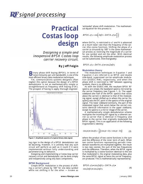
signal processing<strong>Practical</strong><strong>Costas</strong> <strong>loop</strong><strong>design</strong>Designing a simple andinexpensive BPSK <strong>Costas</strong> <strong>loop</strong>carrier recovery circuit.By Jeff Feigin‘antipodal’ phase shift modulation. The mathematicalequation for this process is:⎛π⎞BPSKN( t)= cos fct + DATAN( t)•⎝⎜ 2π⎠⎟2(1)where DATA N is restricted to ±1 and N is advancedat a much lower rate than the frequency of the carrier(the cosine function). Shifting the phase of acarrier (a sinusoid) by 180° is the same mathematicalprocess as reversing the magnitude of a carrierfor one symbol and not the other. With identicalresults, the following amplitude modulation processcan be substituted, interchangeably:BPSKN( t)= DATAN( t)• cos( 2πfct)(2)Modulation theoryThe modulation techniques in Equation 1 andEquation 2 are referred to as BPSK and doubleside-band, suppressed carrier-amplitude modulation(DSBSC-AM), respectively, and when thephase shift is restricted to 180° between opposingsymbols, there is no difference.As with the DSBSC-AM, the resultant BPSK RFspectra are simply the baseband spectra mirrored bythe carrier frequency (see Figures 1, 2). The uppersideband (the half of the BPSK spectra that existsabove the carrier) is identical to that of the modulatingsignal, except shifted up to where the carrier frequencywas the DC point in the spectra of the originalsignal. The lower sideband (similarly, the part of themodulated signal that exists below the carrier) containsidentical information to the upper sideband,except its spectra is a mirror image of the carrier.A mathematically simple demodulation schememultiplies the incoming RF signal by a coherent carrier(a carrier that is identical in frequency andphase to the carrier that originally modulated theBPSK signal). This is an application of the followingtrigonometric identity:1cos( a)• cos( b)= ⎡⎣ cos( a+b)+ cos( a−b)⎤2⎦(3)Figure 1. Amplitude spectra of a typical binary data signal.Binary phase shift keying (BPSK), in terms ofnoise immunity per unit bandwidth, is one of themost efficient binary data modulation techniques.Yet, communications systems <strong>design</strong>ers oftenneglect this option because the <strong>design</strong> of a BPSKdemodulator is not as mathematically simple orstraightforward as frequency shift keying (FSK).The prospect of having to apply thorough engineeringrigor to the <strong>design</strong> of a BPSK demodulator canbe daunting. However, it is unlikely that any suchcircuit will perform as well as it could if it wereimplemented without fully understanding andparameterizing its behavior.Designing and implementing a <strong>Costas</strong>-<strong>loop</strong> carrierrecovery circuit and demodulator can be done simplyand inexpensively using only basic components.where the product of two cosine functions is the sumand the difference of the inner term of each. Whentwo cosine functions representing periodic timedomainwaveforms are multiplied together, the resultis two new cosines; the sum of the two frequenciesand the difference. Therefore, when the BPSK signalis multiplied by a cosine function identical to the onethat modulated it, the original modulating data, plusthe same BPSK signal at twice the carrier frequency,are produced. This is mathematically represented by:BPSK BackgroundSimple BPSK modulation is the process of shiftinga carrier’s phase by 180° for one data symbolwhile not shifting it for the other — known asBPSKN( t)• cos( 2πfct)= DATAN( t)•cos( 2πftc )• cos( 2πftc )(4)20 www.rf<strong>design</strong>.com January 2002
Figure 2. Amplitude spectra of a BPSK modulated carrier .Applying the trigonometric identityfrom Equation 3, the result becomes:1 ⎡DATAN( t)• cos( 0)+ BPSKN( t)•⎤⎢⎥2 ( 2 ft c⎣⎢cos π )⎦⎥(5)Now, considering that the cosine ofzero is one, the result of this multiplicationis the modulating signal plus theBPSK signal shifted to twice its originalfrequency:1DATA t BPSK t 2 f t (6)2⎡⎣ ( )+ ( )• cos( π ) ⎤ N N c ⎦A “brick wall” filter (an ideal lowpassfilter) then isolates the demodulateddata or “low side” product from theextraneous high-frequency or “highside”product:⎡1⎡DATAN( t)+ BPSKN( t)⎤⎤LPF ⎢ ⎢⎥⎥2 • ( 2 ft c⎣⎢⎣⎢cos π )⎦⎥⎦⎥1= DATAN( t)2(7)Equivalently, the block diagram forthis mathematical operation is depictedin Figure 3.Figure 3. Block diagram of an ideal coherentdemodulator .Demodulation theoryOn demodulation, the upper andlower sidebands, which are mirrorimages, will “fold” onto one another.The two sidebands of the modulatingsignal will coherently add while therandom channel noise (in which theupper and lower sidebands are completelyindependent) will randomlyadd. The fact that the two identicalmodulation sidebands coherently addwhile the noise, which occupies theFigure 4. Block diagram of a more easily realizedcoherent receiver.same bandwidth, adds according to aroot mean squared (RMS) relationshipmeans that the demodulated data willhave an inherent signal-to-noise ratio(SNR) advantage, or “processing gain”of 3 dB above that of the BPSK signal.The narrower the bandwidth of thedata filter, the less noise will appear atits output. Too narrow of a filter willlimit demodulated data output levels.For optimum performance, the ratiobetween signal and noise should bemaximized. According to Nyquist’s firstcriteria, so as not interfere with thedata signal at the center of each symbolperiod (the instant where the symbolvalue is decided), a square-shaped“brick wall” filter should have a bandwidthof no less than half the symbolrate. Such a channel filter must haveunity response between DC and a frequencyequal to half the symbol rate.This is the ideal channel filter, becauseit removes the most noise possiblewithout reducing the amplitude of thedesired signal at its sampling instants.It will produce an output SNR that is3dB greater than that of the BPSK signal.Note that Nyquist specifies alternatefilters, vestigial spectrum filtershapes such as the raised-cosine, whichwill achieve the same goal.<strong>Practical</strong> BPSK demodulationThe previous mathematical descriptionexplains the principle behindcoherent BPSK demodulation. Such astructure is straightforward and lendsitself well to understanding the concepts.However, it is difficult to implementthis circuit because its performanceis poor when non-ideal componentsare used. With some modification(see Figure 4), the demodulator circuitbecomes much more practical. Therequirements placed on the buildingblocks of the structure become far lessdemanding to achieve good performance.The more realizable BPSK demodulatoris based on a practical mixer that isallowed to be imperfect. Such a mixercan be built using common semiconductordevices with small current requirements.Unlike an ideal multiplier, easilyimplementable mixers are subject tooverloading and high-order non-linearities;undesired radio signals, whichneed not exist at even similar frequencies,can mix in a complicated mannerto produce undesired interference thatsuperimposes the desired demodulationproduct. The solution is to place a chan-22 www.rf<strong>design</strong>.com January 2002
Figure 5. Resultant data waveform upon ideal vs. practical filtering in a demodulator.Figure 6. A square-then-divide carrier recoverycircuit.nel filter before the mixer to preclude asmuch off-channel energy from reachingthe mixer as possible. The most commoninexpensive channel filters are second-and third-order surface acousticwave (SAW) and ceramic type.However, neither type exhibits idealrectangular characteristics.Low-pass filter discussionsThe low-pass filter, as with the idealdemodulator, is the data filter. Becausethe bandpass filter, ahead of the mixer,removes a great deal of unwantednoise, the low-pass filter requirementscan be relaxed. While the perfectdemodulator requires that the filterexhibit no intersymbol interference (aNyquist filter), the practical <strong>design</strong>may use filters that trade cost, complexity,and size for some degree ofSNR degradation.For the purpose of a simple implementation,a three-pole Butterworth isused as the bandpass filter and a single-poleRC is used as the low-passdata filter for this analysis. The singlepolelow-pass filter has a far more gradualroll-off characteristic than ideal —about –20 dB per frequency decade.Therefore, it will not be possible to minimizeintersymbol interference withFigure 7. A costas <strong>loop</strong> carrier recovery circuit.allowing extra noise through; its –3 dBcutoff point must be defined such thatit maximizes the SNR of the data signal.An optimization means that itsFigure 8. The second-order PLL.bandwidth must be wide enough tominimize ISI, while narrow enough tominimize noise. For an alternating(1,0,1,0,1…) data pattern, a –3 dB cutofffrequency equal to half the symbolrate will maximize SNR for the singlepoleRC low-pass. The total SNR degradation,shown by simulation, is about–1.2 dB for a worst-case alternatingdata pattern, but found to be about–0.6 dB in the case of a random datapattern. This amount of degradation isacceptable for simple <strong>design</strong>s, but betterfilters are recommended if onewishes to improve the SNR.Figure 5 is a comparison of the resultantdemodulated BPSK data on idealand practical demodulation. Idealdemodulation is that of Figure 3 wherethe “perfect filter” is implemented as a10,001-tap raised cosine finite-impulseresponse (FIR) and the practicaldemodulator, from Figure 4, uses aninfinite impulse response (IIR) threepoleButterworth as the channel filterand a one-pole IIR structure as thedata filter. Although the ideal demodulatordoes not faithfully reproduce theoriginal signal, it does reproduce theentire signal to reach its peak value atthe data-sampling instant. This is theonly critical point, according to Nyquist(this is an acausal implementation).However, the result obtained using themore practical structure requires morethan one bit time to reach its maximumlevel. This is the ISI degradation parameter.More noise than ideal wouldhave to be allowed through the demodulatorif one were to attempt to solvethis problem with non-ideal filters.Finally, the carrier must be recovered.Its frequency and phase needs tobe exactly reproduced to optimallydemodulate the BPSK signal. Unlessthere exists some connection or infor-24 www.rf<strong>design</strong>.com January 2002
the BPSK modulation causes ±180°phase transitions, its second harmonicwill be phase-modulated by an ambiguous±360°. The second harmonic is anunmodulated carrier at twice the frequency.Dividing this second harmonicof the carrier by two will result in atheoretically phase-coherent carrier.The advantage of the squaring-thendividecircuit is that it is mathematicallysimple to analyze. However, in practice,controlling the phase offset will besomewhat complicated and layoutdependent;the recovered carrier takesa different path from the demodulatorpath, and this creates a time differentialthat will result in a phase error.Also, several filters are required, makingit difficult to maintain proper phaseover the range operating frequencies.While the first method is a feed-forwardtechnique, the <strong>Costas</strong> <strong>loop</strong> relieson feedback concepts related to thePLL. The <strong>Costas</strong> <strong>loop</strong> offers an inherentability to self-correct the phase (andfrequency) of the recovered carrier and,in the end, its implementation is nomore complicated than the first technique.Its main disadvantage isinvolvement of a <strong>loop</strong> settling time.Figure 9. The output-input phase detection characteristics of multiplier and <strong>Costas</strong>-type phase detection.mation path between the carrier thatwas used in modulation and thedemodulator, a carrier recovery circuitis required for coherent demodulation.Carrier recoveryThe two common methods for BPSKcarrier recovery are: 1) squaring theBPSK signal then dividing by two and2) the 180° <strong>Costas</strong> <strong>loop</strong>. The first techniquerelies on the fact that, becauseAnalyzing the <strong>Costas</strong> LoopThe mechanism of the <strong>Costas</strong> <strong>loop</strong>carrier recovery is to iterate its internallygenerated carrier – the VCO –into the correct phase and frequencybased on the principle of coherency andorthogonality. The low-frequency productof a BPSK signal and its coherentcarrier is the demodulated information,while the low-frequency component iscompletely canceled (there will be nolow-frequency component at all) in thecase of a BPSK signal multiplied by itsorthogonal carrier (a carrier that is 90°out of phase with its coherent carrier).The coherent case has already beenmathematically demonstrated inEquations 3 through 7. For the orthogonalcase, the following trigonometricidentity is presented:cos( a)• sin( b)1= ⎡⎣ sin( a−b)+ sin( a+b)⎤2⎦(8)representing the coherent BPSK carrierat a cosine function and its orthogonalcarrier is a sine (or negative sine)function. The time-domain representationof this orthogonal multiplication is:BPSKN( t)• sin( 2πfct)= DATAN( t)•cos( 2πftc )• sin( 2πftc )(9)Applying the trigonometric identityfrom Equation 8, the result becomes:1 ⎡DATAN( t)• sin( 0)⎤⎢⎥2 + DATAN( t)• ( 2 fc⎣⎢sin π t)⎦⎥(10)Figure 10. VCO tracking behaviors of a <strong>Costas</strong> <strong>loop</strong> and PLL with a BPSK reference input.26 www.rf<strong>design</strong>.com January 2002
Carriers of interestThe carrier that is to become coherentwhen the <strong>loop</strong> settles is represented as acosine function with some phase error.Therefore, the orthogonal carrier thatleads the coherent carrier by 90° must bea negative sine function with the samephase error. Considering the incomingBPSK signal as a cosine with zero phaseoffset relative to time zero, a radial frequencyof ω BPSK , (the radial frequency is2π times the periodic frequency) and the<strong>Costas</strong> <strong>loop</strong> VCO frequency to be ω vcowith a phase error relative to the BPSKcarrier of φ phase_error , the resultant productof the ‘I’ mixer is represented by:I_represented Mixer_Output by:= cos( ωvcot+ θphase _ error)• BPSKN( t)= cos( ωvcot+ θphase _ error)• DATAN( t)• cos( ωbpskt)(13)Figure 11. <strong>Costas</strong> <strong>loop</strong> simulation with a noise-free, band-limited BPSK input.Now, considering that the sine ofzero is zero, the product of this multiplicationis only a “high side” componentand the BPSK signal shifted by90° and to a frequency twice that ofwhat it was.1DATAN( t)• sin( 2πfct)(11)2Next, a low-pass filter removes thehigh-frequency component, and nothingremains:should be equal to avoid imbalancesthat will prolong settling time), it comprisesa pseudo-integrator (a low-passfilter is related to an integrator). Thisallows the circuit to behave in a somewhatsimilar fashion as a second-orderPLL (see Figure 8).For analysis purposes, because themodulating signal is binary data thatreverses its magnitude, DATAN(t) isreplaced by ±1 and the identity ofEquation 3 is applied:1 ⎡cos( ωvco − ωbpsk) t + θphase _ error)+⎤± ⎢⎥2 cos( ωvco + ωbpsk) t + ϑphase_ error⎣⎢) ⎦⎥(14)⎡1⎤LPF • DATAN( t)• ( 2 fct)02⎡⎣⎤ ⎦⎣⎢sin π⎦⎥ =(12)The <strong>Costas</strong> <strong>loop</strong> is “locked” when ithas adjusted its VCO phase and frequency(the initial conditions are random)until the ‘I’ signal is a maximumand the ‘Q’ signal is zero (in reality, thelocked-<strong>loop</strong> ‘Q’ signal is close to zero,but not exactly zero). The third multiplier,the phase doubler, produces theproduct of the ‘I’ and ‘Q’ signals thatsets the VCO input voltage. LPF 3 ’s purposeis only to remove spurious componentsand LPF 1 / LPF 2 “high side” leakage— it is not meant to significantlycontribute to the <strong>loop</strong> response and isoften omitted in theoretical <strong>Costas</strong><strong>loop</strong>s block diagrams. LPF 1 not onlyserves the purpose of a data filter, butin combination with LPF 2 (these twoFigure 12. <strong>Costas</strong> <strong>loop</strong> simulation with a noisy, band-limited BPSK input.28 www.rf<strong>design</strong>.com January 2002
LPF1 removes the “high side” componentand its output; the ‘I’ signal is representedas:1 ⎛( ωvco− ωbpsk)t ⎞LPF 1( t) =± cos2 ⎝⎜+ θphaseerror ⎠⎟_(15)Similarly, the ‘Q’ mixer produces thefollowing product:Q_Mixer_Output= sin( ωvcot + θphase _ error)• BPSKN( t)=− sin( ωvcot+ θphase _ error)• DATAN( t)(16)Applying Equation 8, and again substitutingDATA N (t) with ±1, the resultant‘Q’ product is shown as:1 ⎡sin( ωvco − ωbpsk) t + θphase _ error)+⎤± ⎢⎥2 sin( ωvco + ωbpsk) t + ϑphase_ error⎣⎢) ⎦⎥(17)LPF 2 removes the “high side” componentand its output; the ‘Q’ signal isrepresented as:1 ⎛( ωvco− ωbpsk)t⎞LPF 2( t) =± sin2 ⎝⎜+ θphaseerror ⎠⎟_(18)Further dissectionThe phase detector result is then filteredby LPF 3 , which removes extraneous<strong>loop</strong> products before being appliedto the VCO. Again, this filter is notmeant to significantly contribute to the<strong>Costas</strong> <strong>loop</strong> locking response — itsresponse should be far outside theclosed-<strong>loop</strong> response. From the result ofEquation 21, it can be determined thatthe <strong>loop</strong> will correct itself, both interms of frequency and phase.And, by modifying Equation 21 torepresent absolute phase difference(rather than phases that are relative totime zero), the phase detectionresponse is found.It is important to remember that allthree multipliers compose the phasedetector response. The phase doublermultiplier is not, by itself, “the phasedetector.” In the case where the inputsignals have a peak value of unity, thephase detection response is described byEquation 22. The phase detector gain vs.amplitude dependency is mentioned formathematical completeness, but sucheffects need not be thoroughly quantifiedbecause realistic “multiplier” phasedetectors will be amplitude invariant.Picking unity for the input and VCOamplitudes as the parameters forphase-detector gain serve the purposeof an example gain. The phase-detectionresponse is described by:<strong>Costas</strong> _ Phase _ Detector =1V1− sin ( 2φphase _ difference)≈ Kp= 48r(22)This result is similar to that of a conventionalmultiplier-type phase detectorwhose output, based on a unityamplitude input, is:Conventional _ Phase _ Detector1V= cos ( φphase _ difference)≈ Kp= 2r(23)Comparing these two results (seeFigure 9), the <strong>Costas</strong> <strong>loop</strong> phase detectionresponse is a sine function whilethe multiplier-type phase-detectionresponse is a cosine function of thephase difference. The second-order PLLcontains a low-pass filter that integrates(or pseudo-integrates, dependingon the type of filter) the error signalThen, multiplying these two LPFresults together, the phase doubler produces:Phase _ doubler( t)= LPF • LPF1 2⎡ 1⎤= ± cos ( ωvco −ωbpsk) t + θphase _ error)⎣⎢ 2⎦⎥⎡ 1⎤• ± ( vco − bpsk) t + phase error)⎣⎢ 2 sin ω ω θ _⎦⎥(19)Next, applying Equation 8:⎡sin( 0)⎤1 ⎢⎥=− ⎢ ⎛ ⎛( ωvco− ωbpsk)t⎞⎞ ⎥8+ sin ⎜ 2⎝⎜+ ⎠⎟ ⎟⎣ ⎝ θphase_ error⎢⎠ ⎦⎥(20)Then simplifying the output of thephase doubler, the phase detectorresult becomes:Phase _ det ector _ result =1− sin ( 2( ωvco −ωbpsk) t + θ phase _ error)8(21)Figure 13. Ten <strong>Costas</strong> <strong>loop</strong> settling patterns under identical parameters, but randomized initial conditionsand BPSK modulation data.30 www.rf<strong>design</strong>.com January 2002
from the phase detector. The PLL islocked when the phase detector resultis zero (near zero when the <strong>loop</strong> filter isnot a true integrator), hence producinga DC constant at the input of the VCO.The cosine response of the multiplierphase detector causes a lock when thephase error is 90° (because the cosine of90° is zero).The <strong>Costas</strong> <strong>loop</strong>, considering LPF 1and LPF 2 , acts similarly to a secondorder<strong>loop</strong> (the combined effect of LPF 1and LPF 2 adds a second pole to the <strong>loop</strong>response. The filtered ‘Q’ signal movesjust slightly above or below zero and ismultiplied by the filtered ‘I’ product). Itsdoubled-sine phase detection responseallows two stable locking points: 180°phase error and zero degrees — bothproduce a redundant output that drivesthe VCO to the correct phase/frequency.Low-pass filters LPF 1 /LPF 2 must passthe modulation (the direct result of filtersthat are too narrow is ISI) as:2ω ω 1, 2≥2πBc LP M(24)where B M , the modulation bandwidth,is half the data rate.Before the <strong>loop</strong> has settled, whether aPLL or a <strong>Costas</strong> <strong>loop</strong>, the phase detectionresponse must be one that, basedon the phase relationship between theVCO and the input signal, guides theVCO to a stable locking phase and frequency.If one were to apply a signalwhose phase is reversing by 180° to anordinary PLL, the phase detector resultwould constantly reverse polarity andthe phase error magnitude is unlikely toconverge on any stable value (i.e., thePLL will “track” in opposite directionsfor opposite phases — see Figure 9).One might refer to a conventional phasedetector as 360° periodic. This meansthat the phase of the incoming carrierwould have to be modulated with 360°phase transitions (which is no phasetransition at all because a sinusoidalcarrier has a period of 360°) not to upsetthe tracking so that the <strong>loop</strong> error mayconverge.<strong>Costas</strong> vs. conventionalConversely, the <strong>Costas</strong> <strong>loop</strong> phasedetectionresponse is 180° periodic—there are two stable tracking points.BPSK modulation shifts the <strong>Costas</strong><strong>loop</strong> input by 180°, which is the nextFigure 14. Averaged results of simulation comparing <strong>Costas</strong> <strong>loop</strong> settle time to the bandwidth of LPF3and VCO gain.period of the phase detection function,where the <strong>loop</strong> tracking response isidentical. Therefore, the <strong>Costas</strong> <strong>loop</strong> isable to track a BPSK modulated carrier(<strong>loop</strong>s can also be derived that trackhigher-order phase modulationschemes such as QPSK). The only catchis that the <strong>loop</strong>-phase doubled responsemeans that it has a 50% chance of generatingan upside-down carrier. Figure10 displays simulation results of how a<strong>Costas</strong> <strong>loop</strong> vs. an ordinary PLL withsimilar <strong>loop</strong> parameters would behavewith a BPSK signal as an input.Because LPF 3 is not part of the control<strong>loop</strong> (and not the PLL <strong>loop</strong> filter), itmust not have a frequency responsethat falls within the <strong>loop</strong> bandwidth.Its purpose is only to remove the excessnoise products produced by the threeprevious multipliers and two imperfectfilters. This filter constitutes an undesiredS-plane pole that would cause the<strong>loop</strong> to oscillate, but if its response isfar outside of the <strong>loop</strong> response, then itwill not cause problems. A rule-ofthumbrecommendation for a safe, outof the <strong>loop</strong>, response would be to set thepole of LPF 3 to a minimum of fourtimes that of what the closed <strong>loop</strong>response would be without this filter.Exactly how the VCO will settledepends on the initial phase and frequencyof the VCO as it relates to theincoming BPSK signal, as well as tothe noise characteristics. Althoughnot apparent, the behavior of anypractical implementation of this circuitwill also be affected by the actualdata that has been modulated. Realworldcommunications are usuallyband-limited, and the abrupt 180°phase shifts of BPSK, which the<strong>Costas</strong> <strong>loop</strong> is immune to, wouldrequire an infinite bandwidth.A more realistic-version BPSK signalis one in which a bit transition willcause the carrier amplitude to slowlysweep from its current phase to theopposite phase through the zero-amplitudepoint. The phase-detector contributionto <strong>loop</strong> gain (although realisticphase detectors are not perfect multipliers,they still have minimum inputlevel requirements) is diminished asthe input signal level shrinks.Every BPSK phase transition willcause a <strong>Costas</strong> <strong>loop</strong> “dropout” at andnear the zero-crossing instant duringthe interval between the two discretephase levels. If the <strong>loop</strong> is still in thelocking phase at this point (i.e., whenthe VCO phase does not match that of32 www.rf<strong>design</strong>.com January 2002
pole of this filter equals the closed-<strong>loop</strong>bandwidth. Based on settling time to aparticular threshold, simulation showsthat setting the pole of lag-filter to halfthe DC forward gain results in a quickerlock (this is a point where the <strong>loop</strong> isslightly under-damped). Therefore,these same parameters were used inthe <strong>Costas</strong> <strong>loop</strong> <strong>design</strong> as a startingpoint for simulation.The <strong>Costas</strong> <strong>loop</strong> phase detector gain,under unity input conditions, is 1/4 V/r,as stated in Equation 22, so the VCOgain is the variable that needs to bedetermined. Solving for this parameter,the unity output VCO should have again of eight times the filter’s pole frequency,in terms of radians per secondfor a unity BPSK input for this theoreticalcircuit containing perfect multipliersas the phase detector:Figure 15. Results (interpolated) of simulation of <strong>Costas</strong> <strong>loop</strong> vs. ideal BER performance as input SNRvaries.the carrier), such a “glitch” couldallow a phase slippage and may temporarilyallow the <strong>loop</strong> to track in thewrong direction.Other <strong>design</strong> issues include the effectof realistic (non-ideal) filters. Some“high side” product will always “leak”through and affect the circuit’s performance;their respective responses willnot be identical, and there will be ISI (a1-0-1-0 pattern will not quite produce180° phase transitions). Further, it isnot realistic to assume that the quadraturecomponents of the VCO will have aperfect 90° offset or that the phasedetector is an ideal multiplier free fromDC offset. A second-order PLL analysis(where the <strong>loop</strong> filter is the same asLPF 1 /LPF 2 ) of a carrier will approximatesettling characteristics of a<strong>Costas</strong> <strong>loop</strong>, but a computer simulationis recommended if the <strong>design</strong>er needsaccurate information. This is because“mathematical” building blocks mayneed to be substituted with commonlyavailable and inexpensive components.Figures 11 and 12 show the simulatedtiming waveforms of a <strong>Costas</strong> <strong>loop</strong>operating under noise-free and noisyconditions, respectively.Figure 13 is a plot of the VCO settlingfunction where the <strong>loop</strong> parametersare identical for each run, but theVCO starting phase/frequency and themodulation data are randomized over10 trials. Realistic <strong>Costas</strong> <strong>loop</strong> behavioris somewhat chaotic for the reasonsmentioned previously, depending onwhen BPSK phase transitions occurduring the lock phase.Design considerations of <strong>Costas</strong> <strong>loop</strong>sSimilar to PLL <strong>design</strong>, the <strong>Costas</strong><strong>loop</strong> <strong>design</strong> considerations are noiseperformance, settling time and a reliablelock range. As a demodulator,noise performance is maximized whenthe least amount of noise is allowed inthe <strong>loop</strong>. This is accomplished by settingthe LPF 1 / LPF 2 response to theirmaximum SNR. This corresponds to a–3 dB cutoff equaling half the data ratefor a single-pole RC. For <strong>loop</strong> settlingpurposes, this cutoff is also the minimumallowable for the <strong>loop</strong> filter.Additionally, this is an attractive choicebecause this filter also serves the purposeof a data filter.The <strong>loop</strong> gain must now be set.Because LPF 1 , one of the two identicallegs of the <strong>loop</strong> filter, serves the dualpurpose of also being the data filter andis required to pass BPSK modulation, acompromise has been made. Accordingto [2], the critical damping point (thepoint where minimum settling timeoccurs) for a PLL using the same lagtypefilter as LPF 1 /LPF 2 , is when theVCO _ Gain= 8 • ωLPF1/LPF 2rs// vcritically _ dampedωLPF/ LPF=1K21 2(25)Simulation confirms this result forthe <strong>Costas</strong> <strong>loop</strong> (see Figure 14). Thefastest achievable settle time is one inwhich the VCO has a gain of eighttimes that of the LPF 1 /LPF 2 pole frequencywith the above the phasedetectorgain parameters and a randomBPSK input. Using the <strong>Costas</strong><strong>loop</strong> parameters presented here,where the filter poles and <strong>loop</strong> gainare all in a fixed relationship to thedata rate, the regenerated carrier willsettle in less than three bit times. Ofcourse, if the phase detector has somegain or gain-function other than thatof Equation 22, Equation 25 should beappropriately modified.LPF 3 must then be specified. Thisfilter should have its pole at a lowenoughfrequency that the <strong>Costas</strong> <strong>loop</strong>will not be too noisy nor be subject tocarrier phase reversals in the presenceof noise (the <strong>Costas</strong> <strong>loop</strong> is equally stablein both phases) while high enoughthat it doesn’t cause the <strong>loop</strong> to oscillate.Setting this pole to four times K(or eight times the LPF 1 /LPF 2 pole) isthe point in which this filter will negligiblyaffect on the <strong>loop</strong>; simulationshows this (see Figure 14). To be cautious,particularly at lower data rateswhere such a filter can more easilycreate problems, a factor of six times K(12 times the LPF 1 /LPF 2 pole) is a betterchoice.P34 www.rf<strong>design</strong>.com January 2002
The phase detector and VCO gaincontrol the reliable lock range. With theabove <strong>design</strong> parameters, this <strong>Costas</strong><strong>loop</strong> will always reliably lock so long asthe VCO can produce the required carrierfrequency. This value, the frequencyrange in which the <strong>loop</strong> may lock, isdetermined as follows:Range ≈ Gain _ • GainVCO phase detector VCO(26)A more practical limit on how far thecarrier recovery circuit may “stretch”from its center frequency, however,depends on the width of the band-passfilter shown in Figure 4. Whatever thetrack and hold ability of the <strong>Costas</strong><strong>loop</strong>, the carrier recovery range willnever reach beyond that of the intermediatefrequency (IF) filters.Finally, noise performance must beconsidered. While demodulated BPSK(the data, itself) has an SNR that is3 dB greater than that of the modulatedBPSK (not considering ISI degradationdue to non-ideal filtering), noisewill cause the <strong>Costas</strong> <strong>loop</strong> to introduceeven more noise of its own.The reason is that a carrier recoverycircuit produces a noisy carrier undernoisy conditions. Figure 15 displaysthe bit error rate (BER) performanceof ideal BPSK demodulation (Figure 3)vs. practical demodulation with idealcarrier recovery (Figure 4) vs. <strong>Costas</strong><strong>loop</strong> demodulation, with a randomdata pattern. It is observed that this<strong>Costas</strong> <strong>loop</strong> demodulator performs wellat regenerating the carrier until a lowSNR input. At a BER of 10 –4 (a valueoften specified for minimum systemperformance), non-ideal filtering contributesa 1.5 dB degradation while<strong>Costas</strong> non-ideal carrier recovery causesonly an additional 0.6 db demodulatorloss. It is clear that, in the overallscheme, single-pole data filtering causesmore SNR degradation than a<strong>Costas</strong> <strong>loop</strong>.Implementation discussionThe most difficult structure to implementin a <strong>Costas</strong> <strong>loop</strong>, within reasonablecost, complexity, and performance,is a quadrature downconverter. Such acircuit requires that the incomingBPSK signal be split between two mixers(to perform the down-conversionmultiplication) and independently multipliedby two signals of identical frequency,but differ in phase by 90°.The greatest difficulty arises fromproducing these two signals as well asmaintaining their relative phase offsetover a range of frequencies. Fortunately,modern integrated circuits provide aneasy-to-use and inexpensive implementationof an I/Q demodulator. Such ICsare also attractive solutions becausethey provide additional mixers andamplifiers that facilitate the necessarybuilding blocks required to build most ofa receiver.The remaining <strong>Costas</strong> <strong>loop</strong> buildingblocks are three low-pass filters, the“phase doubler” multiplier, and a single-phaseVCO. As previously mentioned,all filters in this <strong>design</strong> are single-poleRC (this is for simplicity—thereader may wish to implement othertypes of filters for better performance).One can implement the multiplierand VCO in a number of ways. The useof an integrated op amp-type multiplierand a separate VCO are one possibility.A double-balanced switching-typemixer is also a suitable choice, althoughits pseudo-multiplier characteristicswill somewhat alter the <strong>Costas</strong> <strong>loop</strong>characteristics. However, conventionalPLL logic gate phase detectors (such asthe XOR) or devices that must be operatedunder heavy saturation (whichcauses limiting) are unsuitable. Devicesthat limit the Q-channel, but not the I-channel are perfectly acceptable.ConclusionsThe <strong>Costas</strong> <strong>loop</strong>, a cousin of thePLL, is an effective close-<strong>loop</strong> coherentdemodulator. Though the PLL and<strong>Costas</strong> <strong>loop</strong> exhibit similar settingcharacteristics when configured underidentical parameters, the latter canlock onto a carrier that is reversing inphase; A <strong>Costas</strong> <strong>loop</strong> regenerates the“phantom” BPSK carrier. Predictionof settling behavior may be estimatedby appropriately substituting <strong>Costas</strong><strong>loop</strong> parameters into a traditionalPLL analysis, but simulation isrequired to accurately estimate itschaotic behavior.Based on simulation, <strong>Costas</strong> <strong>loop</strong>settling time is minimized when theclosed-<strong>loop</strong> bandwidth is twice that ofits constituent RC filter, according to aslightly under-damped condition. Ithas also been found that a filter afterthe phase-doubler multiplier (the thirdmultiplier) is effective in reducing <strong>loop</strong>noise when its response is kept faroutside of the closed-<strong>loop</strong> bandwidth.Finally, referring to Figure 15,although the recovered carrier is noisywhen a <strong>Costas</strong> <strong>loop</strong> is presented with anoisy BPSK signal, the ISI created bysimple data filters produces the mostdegradation in a simple <strong>Costas</strong> <strong>loop</strong>implementation.References[1] F. M. Gardner, “PhaselockTechnique,” Wiley, New York, 1979.[2] B.P. Lathi, “Modern Digital andAnalog Communications Systems 2ndEdition,” Oxford University Press, NewYork, 1983.About the authorJeffrey Feigin is an RF applicationsengineer at Analog Devices,where his responsibilities include RFIC applications support, systemslevelIC <strong>design</strong> and reference <strong>design</strong>.Previously, Feigin was a <strong>design</strong> engineerwith Zo&Co., in Skopje,Macedonia, where he <strong>design</strong>ed microcontrollerand RF circuitry for anurban wireless network. Prior to that,he was employed at Lincom Corp. asa contract engineer, where he developedan OPNET model of a TCP/IPover Milstar. In addition, while aresearch assistant at the Center forWireless Information NetworkStudies, Feigin performed QoS analysisof wireless multimedia Internettraffic and protocols. Feigin is a graduateof Worcester PolytechnicInstitute with a B.S.E.E. andM.S.E.E. For further information,contact Doug Grantdoug.grant@analog.com36 www.rf<strong>design</strong>.com January 2002