Designing an RFIC CMOS upconversion mixer - Mobile Dev & Design
Designing an RFIC CMOS upconversion mixer - Mobile Dev & Design
Designing an RFIC CMOS upconversion mixer - Mobile Dev & Design

Create successful ePaper yourself
Turn your PDF publications into a flip-book with our unique Google optimized e-Paper software.
design software<br />
<strong><strong>Design</strong>ing</strong> <strong>an</strong><br />
<strong>RFIC</strong> <strong>CMOS</strong><br />
<strong>upconversion</strong> <strong>mixer</strong><br />
Software to help the engineer design<br />
<strong>an</strong>d implement a <strong>CMOS</strong> <strong>mixer</strong><br />
on <strong>an</strong> <strong>RFIC</strong> platform —<br />
issues, tradeoffs <strong>an</strong>d solutions.<br />
By Stephen Long<br />
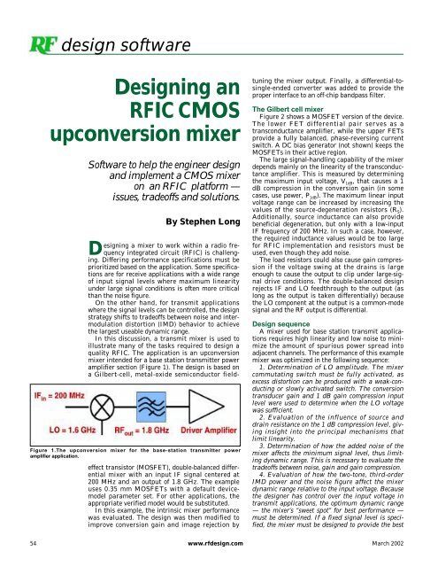
Figure 1.The <strong>upconversion</strong> <strong>mixer</strong> for the base-station tr<strong>an</strong>smitter power<br />
amplifier application.<br />
<strong><strong>Design</strong>ing</strong> a <strong>mixer</strong> to work within a radio frequency<br />
integrated circuit (<strong>RFIC</strong>) is challenging.<br />
Differing perform<strong>an</strong>ce specifications must be<br />
prioritized based on the application. Some specifications<br />
are for receive applications with a wide r<strong>an</strong>ge<br />
of input signal levels where maximum linearity<br />
under large signal conditions is often more critical<br />
th<strong>an</strong> the noise figure.<br />
On the other h<strong>an</strong>d, for tr<strong>an</strong>smit applications<br />
where the signal levels c<strong>an</strong> be controlled, the design<br />
strategy shifts to tradeoffs between noise <strong>an</strong>d intermodulation<br />
distortion (IMD) behavior to achieve<br />
the largest useable dynamic r<strong>an</strong>ge.<br />
In this discussion, a tr<strong>an</strong>smit <strong>mixer</strong> is used to<br />
illustrate m<strong>an</strong>y of the tasks required to design a<br />
quality <strong>RFIC</strong>. The application is <strong>an</strong> <strong>upconversion</strong><br />
<strong>mixer</strong> intended for a base station tr<strong>an</strong>smitter power<br />
amplifier section (Figure 1). The design is based on<br />
a Gilbert-cell, metal-oxide semiconductor fieldeffect<br />
tr<strong>an</strong>sistor (MOSFET), double-bal<strong>an</strong>ced differential<br />
<strong>mixer</strong> with <strong>an</strong> input IF signal centered at<br />
200 MHz <strong>an</strong>d <strong>an</strong> output of 1.8 GHz. The example<br />
uses 0.35 mm MOSFETs with a default devicemodel<br />
parameter set. For other applications, the<br />
appropriate verified model would be substituted.<br />
In this example, the intrinsic <strong>mixer</strong> perform<strong>an</strong>ce<br />
was evaluated. The design was then modified to<br />
improve conversion gain <strong>an</strong>d image rejection by<br />
tuning the <strong>mixer</strong> output. Finally, a differential-tosingle-ended<br />
converter was added to provide the<br />
proper interface to <strong>an</strong> off-chip b<strong>an</strong>dpass filter.<br />
The Gilbert cell <strong>mixer</strong><br />
Figure 2 shows a MOSFET version of the device.<br />
The lower FET differential pair serves as a<br />
tr<strong>an</strong>sconduct<strong>an</strong>ce amplifier, while the upper FETs<br />
provide a fully bal<strong>an</strong>ced, phase-reversing current<br />
switch. A DC bias generator (not shown) keeps the<br />
MOSFETs in their active region.<br />
The large signal-h<strong>an</strong>dling capability of the <strong>mixer</strong><br />
depends mainly on the linearity of the tr<strong>an</strong>sconduct<strong>an</strong>ce<br />
amplifier. This is measured by determining<br />
the maximum input voltage, V 1dB , that causes a 1<br />
dB compression in the conversion gain (in some<br />
cases, use power, P 1dB ). The maximum linear input<br />
voltage r<strong>an</strong>ge c<strong>an</strong> be increased by increasing the<br />
values of the source-degeneration resistors (R S ).<br />
Additionally, source induct<strong>an</strong>ce c<strong>an</strong> also provide<br />
beneficial degeneration, but only with a low-input<br />
IF frequency of 200 MHz. In such a case, however,<br />
the required induct<strong>an</strong>ce values would be too large<br />
for <strong>RFIC</strong> implementation <strong>an</strong>d resistors must be<br />
used, even though they add noise.<br />
The load resistors could also cause gain compression<br />
if the voltage swing at the drains is large<br />
enough to cause the output to clip under large-signal<br />
drive conditions. The double-bal<strong>an</strong>ced design<br />
rejects IF <strong>an</strong>d LO feedthrough to the output (as<br />
long as the output is taken differentially) because<br />
the LO component at the output is a common-mode<br />
signal <strong>an</strong>d the RF output is differential.<br />
<strong>Design</strong> sequence<br />
A <strong>mixer</strong> used for base station tr<strong>an</strong>smit applications<br />
requires high linearity <strong>an</strong>d low noise to minimize<br />
the amount of spurious power spread into<br />
adjacent ch<strong>an</strong>nels. The perform<strong>an</strong>ce of this example<br />
<strong>mixer</strong> was optimized in the following sequence:<br />
1. Determination of LO amplitude. The <strong>mixer</strong><br />
commutating switch must be fully activated, as<br />
excess distortion c<strong>an</strong> be produced with a weak-conducting<br />
or slowly activated switch. The conversion<br />
tr<strong>an</strong>sducer gain <strong>an</strong>d 1 dB gain compression input<br />
level were used to determine when the LO voltage<br />
was sufficient.<br />
2. Evaluation of the influence of source <strong>an</strong>d<br />
drain resist<strong>an</strong>ce on the 1 dB compression level, giving<br />
insight into the principal mech<strong>an</strong>isms that<br />
limit linearity.<br />
3. Determination of how the added noise of the<br />
<strong>mixer</strong> affects the minimum signal level, thus limiting<br />
dynamic r<strong>an</strong>ge. This is necessary to evaluate the<br />
tradeoffs between noise, gain <strong>an</strong>d gain compression.<br />
4. Evaluation of how the two-tone, third-order<br />
IMD power <strong>an</strong>d the noise figure affect the <strong>mixer</strong><br />
dynamic r<strong>an</strong>ge relative to the input voltage. Because<br />
the designer has control over the input voltage in<br />
tr<strong>an</strong>smit applications, the optimum dynamic r<strong>an</strong>ge<br />
— the <strong>mixer</strong>’s “sweet spot” for best perform<strong>an</strong>ce —<br />
must be determined. If a fixed signal level is specified,<br />
the <strong>mixer</strong> must be designed to provide the best<br />
54 www.rfdesign.com March 2002
Figure 2. The MOSFET Gilbert-cell active doublebal<strong>an</strong>ced<br />
<strong>mixer</strong>.<br />
dynamic r<strong>an</strong>ge at that signal level.<br />
5. Finally, testing the <strong>mixer</strong> under a<br />
realistic signal input, such as a CDMA<br />
source, to emulate a multicarrier environment.<br />
This is a more severe test th<strong>an</strong><br />
the two-tone IMD. It is also much more<br />
time consuming to simulate because a<br />
large number of symbols must be used<br />
for accurate results.<br />
Once the basic resistively loaded<br />
Gilbert cell <strong>mixer</strong> was characterized, two<br />
modifications were used to improve perform<strong>an</strong>ce.<br />
First, the <strong>mixer</strong> drain nodes<br />
were tuned with inductors <strong>an</strong>d a capacitor<br />
for reson<strong>an</strong>ce at the output frequency.<br />
This improves conversion gain if inductors<br />
with reasonable Q c<strong>an</strong> be fabricated.<br />
It also decreases the amplitude of the<br />
undesired output image signal because of<br />
its b<strong>an</strong>dpass tr<strong>an</strong>sfer function. The image<br />
must be removed <strong>an</strong>yway, <strong>an</strong>d its presence<br />
c<strong>an</strong> only degrade the distortion of<br />
the output stage by increasing the peak<br />
voltage present at its input.<br />
The other ch<strong>an</strong>ge was to convert the<br />
differential signal to single-ended.<br />
Because the output of the <strong>mixer</strong> must be<br />
filtered off-chip with a surface acoustic<br />
wave (SAW) filter before further amplification,<br />
a single-ended output is more<br />
efficient. The circuit must have good<br />
common-mode rejection to suppress LO<br />
feedthrough <strong>an</strong>d good linearity so that it<br />
doesn’t degrade dynamic r<strong>an</strong>ge.<br />
Determining LO voltage<br />
Once the topology was established, the<br />
first step in designing this <strong>mixer</strong> was to<br />
determine a suitable LO voltage. The LO<br />
level should provide a reasonable compromise<br />
between conversion gain <strong>an</strong>d<br />
LO power but should not limit the 1 dB<br />
gain-compression input voltage. The<br />
MOSFETs forming the commutating<br />
switch (upper level) must be driven hard<br />
enough to present a low series resist<strong>an</strong>ce<br />
to the load. An LO power sweep <strong>an</strong>d <strong>an</strong><br />
N dB gain compression <strong>an</strong>alysis c<strong>an</strong> be<br />
used to evaluate the dependence of gain<br />
compression on the LO drive.<br />
Figure 3. Differential <strong>mixer</strong> simulation setup.<br />
The simulation setup for the initial<br />
<strong>mixer</strong> design is shown in Figure 3. For<br />
simplicity, the <strong>mixer</strong> is implemented as<br />
a sub-network. As such, the <strong>mixer</strong> itself<br />
c<strong>an</strong> be replaced or modified as necessary<br />
throughout the design process<br />
while maintaining the basic simulation<br />
setup. Mixer parameters are accessible<br />
outside the sub-network <strong>an</strong>d are passed<br />
to the <strong>mixer</strong> design for <strong>an</strong>alysis. In this<br />
example, drain voltage (V DD ), drain<br />
resist<strong>an</strong>ce (R D ), current-source control<br />
width (Wcsp), tr<strong>an</strong>sconduct<strong>an</strong>ce <strong>an</strong>d<br />
switch MOSFET widths (W 1 <strong>an</strong>d W 2 ),<br />
source-degeneration resist<strong>an</strong>ce (R S ), <strong>an</strong>d<br />
source-degeneration induct<strong>an</strong>ce (L S ) are<br />
all available for parameter sweeps.<br />
The simulations showed that the<br />
input power at which gain compresses<br />
by 1 dB (P 1dB ) does not have a strong<br />
dependence on LO voltage, but conversion<br />
gain does depend somewhat on LO<br />
voltage (Figure 4). As more gate voltage<br />
is applied to the upper pair of<br />
MOSFETs, their series resist<strong>an</strong>ce<br />
becomes lower relative to the drain<br />
resist<strong>an</strong>ce <strong>an</strong>d, thus, the conversion<br />
gain is higher. A conversion loss worsened<br />
at the higher output RF frequency<br />
of 1.8 GHz, but this could be improved<br />
by tuning the RF output of the <strong>mixer</strong>.<br />
Gain compression evaluation<br />
Next, gain compression was evaluated.<br />
The 1 dB gain compression input power<br />
<strong>an</strong>d input voltage were found for a r<strong>an</strong>ge<br />
of swept parameters. For this example,<br />
we w<strong>an</strong>ted to know the influence of R S<br />
<strong>an</strong>d R D on V 1dB . The R S sweep used <strong>an</strong> R D<br />
of 100Ω, <strong>an</strong>d the R D sweep set used <strong>an</strong> R S<br />
of 30Ω. Conversion gain was measured at<br />
the 1 dB compressed level.<br />
V 1dB , rather th<strong>an</strong> P 1dB , is used as the<br />
input signal level parameter. In <strong>an</strong><br />
<strong>RFIC</strong> <strong>mixer</strong>, where the input might not<br />
be matched to a source imped<strong>an</strong>ce, the<br />
input voltage is a more import<strong>an</strong>t metric<br />
of gain compression th<strong>an</strong> the input<br />
power because available power assumes<br />
a conjugate match between source <strong>an</strong>d<br />
load. Also, in a multisignal environment,<br />
the peak input voltage c<strong>an</strong> be quite large<br />
at the inst<strong>an</strong>t in time when all signals<br />
add in phase. It is this peak voltage that<br />
determines the distortion limits of the<br />
<strong>mixer</strong>. For example, two-tone IMD simulations<br />
predicted a 1 dB compression<br />
power that was 6 dB lower th<strong>an</strong> predict-<br />
LO Power LO voltage 1.0 dB gain compression Conversion<br />
dBm @LO freq input power level (dBm) gain<br />
0.000 0.589 / -22.529 -6.825 -9.721<br />
2.000 0.743 / -21.791 -6.891 -9.305<br />
4.000 0.938 / -21.168 -6.924 -8.993<br />
6.000 1.182 / -20.657 -6.957 -8.753<br />
Figure 4. Simulations showing the effects of LO voltage on the input power at which gain compresses by<br />
1 dB, <strong>an</strong>d conversion gain.<br />
56 www.rfdesign.com March 2002
Figure 5. The effects of input voltage on dynamic r<strong>an</strong>ge.<br />
ed by single-tone simulations because<br />
the peak voltage was twice as high for<br />
the same power per tone.<br />
It is also noteworthy that the conversion<br />
power gain varies inversely with the<br />
value of RD. In the simulation, the external<br />
load resist<strong>an</strong>ce was set to 2R D so that<br />
the output power (power absorbed by the<br />
load) was also the available output<br />
power, P out = V out2 /R D . The voltage gain<br />
would be expected to follow R D /R S , but<br />
increased less rapidly th<strong>an</strong> <strong>an</strong>ticipated,<br />
probably due to the output RC time-const<strong>an</strong>t<br />
b<strong>an</strong>dwidth limitations.<br />
Determining noise tradeoffs<br />
The next step was to evaluate how<br />
DC bias current (I_bias) <strong>an</strong>d source<br />
resist<strong>an</strong>ce affect the <strong>mixer</strong> noise figure.<br />
The <strong>mixer</strong>’s single-sideb<strong>an</strong>d noise figure<br />
(SSB NF) was simulated as a function<br />
of DC bias current through the<br />
Gilbert cell (<strong>mixer</strong> core). The DC current<br />
was varied by sweeping the width<br />
of the PMOS current source (W csp ) <strong>an</strong>d<br />
the <strong>mixer</strong> current mirror width (W cs )<br />
using a parameter sweep.<br />
The SSB NF was appropriate<br />
because only one input frequency was<br />
applied to the <strong>mixer</strong>, but wideb<strong>an</strong>d<br />
noise at the image frequency <strong>an</strong>d from<br />
LO harmonics was included in the signal-to-noise<br />
calculation. The simulation<br />
showed that the NF was reduced with<br />
increasing I_bias, but reached a point<br />
of diminishing returns. Thus, a width<br />
of 50 µm for the current source was<br />
selected as a compromise between<br />
power <strong>an</strong>d noise.<br />
The SSB NF was also found to<br />
strongly depend on the source resist<strong>an</strong>ce.<br />
This was expected because the<br />
thermal noise contributed by the resistor<br />
is directly in the input voltage loop<br />
of the differential pair. Thus, there<br />
needs to be a tradeoff between V 1dB <strong>an</strong>d<br />
NF to obtain the largest dynamic r<strong>an</strong>ge<br />
of the <strong>mixer</strong>.<br />
The carrier-to-noise ratio limits the<br />
dynamic r<strong>an</strong>ge at low input signal<br />
power levels. The noise power for a<br />
minimum detectable signal (S/N = 1)<br />
depends on both NF <strong>an</strong>d the noise<br />
b<strong>an</strong>dwidth. This b<strong>an</strong>dwidth is normally<br />
set by <strong>an</strong> external SAW filter between<br />
the <strong>mixer</strong> <strong>an</strong>d the driver amplifier. The<br />
filter is also required to reject the output<br />
difference (F LO – F in ) image frequency<br />
at 1.4 GHz.<br />
The conversion gain (or loss in this<br />
case) may also increase the noise figure<br />
because the drain resistor’s thermal<br />
noise is input-referred through the<br />
gain. If the design goals require it, a<br />
tuned output should be investigated to<br />
eliminate some of this noise.<br />
At higher input signal levels, the<br />
dynamic r<strong>an</strong>ge of the <strong>mixer</strong> is limited<br />
by distortion. The third-order IMD<br />
products are the most damaging<br />
because they show up in-b<strong>an</strong>d <strong>an</strong>d c<strong>an</strong>not<br />
be rejected by the filter. A two-tone,<br />
third-order IMD simulation with <strong>an</strong> RF<br />
power sweep was used to display the<br />
carrier-to-IMD power ratio. The IMD<br />
power present in the output increases<br />
at three times the rate of increase of<br />
input power. Thus, the difference<br />
between output power <strong>an</strong>d IMD power<br />
shrinks with increasing input.<br />
Dynamic r<strong>an</strong>ge vs. input voltage<br />
Determining the effect of input voltage<br />
on dynamic r<strong>an</strong>ge required the output<br />
from two simulations: IMD RF<br />
power sweep <strong>an</strong>d the SSB NF (see<br />
Figure 5). The dynamic r<strong>an</strong>ge is controlled<br />
by the least of these two conditions<br />
(see Table 1):<br />
R S D R (dB) V in (V) NF (dB)<br />
(differential)<br />
10 57.7 0.017 6.5<br />
20 57.3 0.025 8<br />
30 56.4 0.031 9.2<br />
40 56.0 0.039 10.3<br />
Table 1. Dynamic r<strong>an</strong>ge vs. input voltage.<br />
Figure 6. The differential amplifier stage used to<br />
the differential output to single-ended.<br />
• DR = P out (dBm) – MDS (dBm) (noiselimited<br />
for low input levels).<br />
• DR = P out (dBm) – P IMD (dBm) (distortion-limited<br />
for higher input levels).<br />
The dynamic r<strong>an</strong>ge peak depends on<br />
the noise b<strong>an</strong>dwidth. For narrower<br />
b<strong>an</strong>dwidths, the noise floor drops <strong>an</strong>d<br />
the peak D R increases but shifts to<br />
lower differential input voltage.<br />
Because of the base-station application,<br />
where the tr<strong>an</strong>smitter should be<br />
capable of covering <strong>an</strong> entire frequency<br />
b<strong>an</strong>d, a 30 MHz noise b<strong>an</strong>dwidth<br />
was chosen.<br />
Tuning <strong>mixer</strong> drain nodes<br />
The low conversion gain of the resistively<br />
loaded <strong>mixer</strong> caused higher<br />
noise due to the drain resistors. By<br />
resonating the output at 1.8 GHz, the<br />
conversion gain was increased <strong>an</strong>d the<br />
gain at the image (1.4 GHz) was<br />
reduced. A comparison between the<br />
resistively loaded case <strong>an</strong>d the tuned<br />
case showed <strong>an</strong> increase in conversion<br />
gain of about 3.5 dB.<br />
To find the reson<strong>an</strong>t frequency of a<br />
specific design, perform <strong>an</strong> RF frequency<br />
sweep. From that, it is possible to<br />
calculate how much capacit<strong>an</strong>ce is contributed<br />
by the drain-to-substrate junction<br />
<strong>an</strong>d absorb it into the resonator.<br />
Gain reduction due to inductor Q<br />
In bulk silicon processes, on-chip<br />
inductor Q is limited by metal losses<br />
<strong>an</strong>d substrate conduction. An ordinary<br />
digital IC process produces low Q in<br />
spiral inductors. <strong>CMOS</strong> or Bi<strong>CMOS</strong><br />
<strong>RFIC</strong> processes c<strong>an</strong> achieve higher Q<br />
inductors by using thicker dielectrics<br />
<strong>an</strong>d thicker metal. Q values in the<br />
r<strong>an</strong>ge of 5 to 15 are typical.<br />
Unfortunately, for realistic unloaded<br />
inductor Q values on the order of 5, the<br />
benefits of tuned output are diminished.<br />
58 www.rfdesign.com March 2002
Figure 7. Noise figure <strong>an</strong>d conversion gain contours.<br />
Figure 8. A single-ended <strong>mixer</strong> modified to evaluate the designed <strong>mixer</strong>.<br />
The conversion gain is improved by<br />
about 4 dB, but the noise figure is<br />
improved by only 0.5 dB. A tuned output<br />
would be of greater benefit on a <strong>CMOS</strong><br />
RF <strong>an</strong>alog, silicon-on-insulator (SOI), or<br />
gallium-arsenide (GaAs) process, where<br />
higher Q values c<strong>an</strong> be obtained.<br />
Differential-to-S-E conversion<br />
The next step in the design was to<br />
convert the RF output from differential<br />
to single-ended with <strong>an</strong> active balun.<br />
Rather th<strong>an</strong> taking one output from the<br />
<strong>mixer</strong>, this conversion is required to<br />
maintain a differential output, which is<br />
necessary for rejection of LO<br />
feedthrough. A single-ended output is<br />
sufficient to drive the SAW filter that is<br />
needed between the <strong>mixer</strong> output <strong>an</strong>d<br />
the driver stage. Although passive<br />
baluns c<strong>an</strong> be made for 1.8 GHz frequency<br />
devices, placing <strong>an</strong> active balun<br />
on-chip provides cost <strong>an</strong>d size benefits.<br />
The differential amplifier stage<br />
shown in Figure 6 converts the differential<br />
output of the tuned <strong>mixer</strong> to a single-ended<br />
output. The gate capacit<strong>an</strong>ces<br />
of the differential-to-single-ended<br />
(D2SE) stage c<strong>an</strong> be absorbed into the<br />
resonator at the <strong>mixer</strong> drain nodes.<br />
Also, the D2SE stage must be designed<br />
so that it does not dominate the IMD<br />
generation of the <strong>mixer</strong>. R S _D2SE c<strong>an</strong><br />
be adjusted to set the V 1dB level.<br />
The output driver c<strong>an</strong> use <strong>an</strong> off-chip<br />
load resist<strong>an</strong>ce with <strong>an</strong> open-drain output<br />
connection, as suggested by Figure<br />
6. The load resist<strong>an</strong>ce would then be<br />
determined either by the filter imped<strong>an</strong>ce<br />
or by a tr<strong>an</strong>smission line imped<strong>an</strong>ce,<br />
which would then dictate the bias<br />
current for the D2SE converter stage.<br />
The device widths must also be chosen<br />
so that they c<strong>an</strong> h<strong>an</strong>dle the necessary<br />
drain current <strong>an</strong>d provide adequate<br />
60 www.rfdesign.com March 2002
Figure 9. The dynamic r<strong>an</strong>ge peak at 57.5 dB is obtained at a input level of 14 mV.<br />
voltage gain. The addition of a source<br />
follower to the output is <strong>an</strong>other option.<br />
<strong>Design</strong> evaluation<br />
For the initial design evaluation, it<br />
was easier to measure the differential<br />
output so that tradeoffs <strong>an</strong>d comparisons<br />
could be made between the differential<br />
tuned <strong>mixer</strong> <strong>an</strong>d the <strong>mixer</strong><br />
with <strong>an</strong> output buffer. Once the<br />
design was complete, the <strong>mixer</strong> could<br />
then be evaluated in a single-ended<br />
configuration.<br />
The SSB NF simulation was performed<br />
again with parameter sweeps<br />
for R S <strong>an</strong>d R ind . Figure 7 shows that<br />
there is little noise sensitivity to R ind ;<br />
however, it strongly affects the conversion<br />
gain. R S affects both NF <strong>an</strong>d conversion<br />
gain as well as the carrier-to-<br />
IMD ratio vs. IF input voltage. The<br />
<strong>mixer</strong> TOI/IMD simulation was performed<br />
again for <strong>an</strong> R S of 10, 20, <strong>an</strong>d<br />
30Ω. The dynamic r<strong>an</strong>ge slowly<br />
improves for smaller R S , but is dependent<br />
on the noise b<strong>an</strong>dwidth.<br />
To speed up the process, a stock<br />
schematic intended for evaluation of<br />
single-ended <strong>mixer</strong>s was copied from<br />
the menu <strong>an</strong>d modified as shown in<br />
Figure 8. The tuned <strong>mixer</strong> with the<br />
D2SE output stage was then inserted<br />
from the component library. Unused<br />
inputs were terminated, the input was<br />
grounded <strong>an</strong>d the output terminated in<br />
a large resist<strong>an</strong>ce. To obtain a differential<br />
LO, a tr<strong>an</strong>sformer <strong>an</strong>d source were<br />
copied from a differential test schematic<br />
<strong>an</strong>d pasted into this schematic. An<br />
active LO single-ended-to-differential<br />
stage could also be designed <strong>an</strong>d added<br />
to the <strong>mixer</strong>.<br />
Again, NF <strong>an</strong>d IMD vs. RF power<br />
sweeps were performed for a r<strong>an</strong>ge of<br />
RS values from 10 to 30Ω. This was<br />
combined to determine dynamic r<strong>an</strong>ge,<br />
plotted in Figure 9. An R S of 10Ω produced<br />
the best result: a peak dynamic<br />
62 www.rfdesign.com March 2002
<strong>an</strong>ge of 57.5 dB at <strong>an</strong> input voltage of<br />
14 mV.<br />
Pushing toward reality<br />
Simulation with a digital signal<br />
source such as CDMA is a more severe<br />
test of linearity. An IS-95 CDMA<br />
source with good adjacent-ch<strong>an</strong>nel<br />
power ratio (ACPR) was used to drive<br />
the <strong>mixer</strong> input. When the input RF<br />
signal level was set to the optimum<br />
value for <strong>mixer</strong> dynamic r<strong>an</strong>ge, little<br />
spectral regrowth was observed.<br />
The input of the <strong>mixer</strong> is badly mismatched,<br />
which may not be of much<br />
concern if the baseb<strong>an</strong>d <strong>an</strong>d IF driver<br />
circuits are on the same chip with the<br />
<strong>upconversion</strong> <strong>mixer</strong>. In that case, the<br />
voltage levels are of greater interest. If<br />
the <strong>mixer</strong> is driven from off-chip circuitry,<br />
the input imped<strong>an</strong>ce will be<br />
dominated by capacitive react<strong>an</strong>ce <strong>an</strong>d<br />
a matching network could signific<strong>an</strong>tly<br />
increase the conversion gain.<br />
Summary<br />
This study of the design <strong>an</strong>d optimization<br />
of <strong>an</strong> <strong>RFIC</strong> <strong>upconversion</strong> tr<strong>an</strong>smit<br />
About the author<br />
Stephen Long received his B.S. degree in engineering physics from UC<br />
Berkeley <strong>an</strong>d his M.S. <strong>an</strong>d PhD in electrical engineering from Cornell University.<br />
He has been a professor of electrical <strong>an</strong>d computer engineering at UC S<strong>an</strong>ta<br />
Barbara since 1981. The theme of his current research projects is practical: Use<br />
unconventional digital <strong>an</strong>d <strong>an</strong>alog circuits, high-perform<strong>an</strong>ce devices <strong>an</strong>d fabrication<br />
technologies to address signific<strong>an</strong>t problems in high-speed electronics such as<br />
low-power IC interconnections, high-speed digital ICs, <strong>an</strong>d microwave <strong>an</strong>alog<br />
integrated circuits for RF communications. He teaches classes on communication<br />
electronics <strong>an</strong>d high-speed digital IC design.<br />
Prior to joining UCSB, from 1974 to 1977 he was a senior engineer at<br />
Vari<strong>an</strong> Associates, Palo Alto, CA. From 1978 to 1981 he was employed by<br />
Rockwell International Science Center, Thous<strong>an</strong>d Oaks, CA as a member of<br />
the technical staff.<br />
Long received the IEEE Microwave Applications Award in 1978 for development<br />
of InP millimeter wave devices. In 1988 he was a research visitor at GEC<br />
Hirst Research Centre, U.K. In 1994 he was a Fulbright research visitor at the<br />
Signal Processing Laboratory, Tampere University of Technology, Finl<strong>an</strong>d <strong>an</strong>d a<br />
visiting professor at the Electromagnetics Institute, Technical University of<br />
Denmark. He is a senior member of the IEEE <strong>an</strong>d a member of the Americ<strong>an</strong><br />
Scientific Affiliation.<br />
<strong>mixer</strong> shows how design <strong>an</strong>d <strong>an</strong>alysis<br />
tools c<strong>an</strong> help the designer evaluate the<br />
perform<strong>an</strong>ce of these devices <strong>an</strong>d determine<br />
ways to improve them.<br />
The <strong>mixer</strong> design presented in this<br />
paper was achieved using the Mixer<br />
<strong>Design</strong>Guide in Agilent EEsof EDA’s<br />
Adv<strong>an</strong>ced <strong>Design</strong> System 2001 (ADS<br />
2001). The Mixer <strong>Design</strong>Guide was used<br />
to create simulation setups, data displays<br />
<strong>an</strong>d imped<strong>an</strong>ce matching.<br />
64 www.rfdesign.com March 2002