LNA Matching Techniques for Optimizing Noise Figures
LNA Matching Techniques for Optimizing Noise Figures
LNA Matching Techniques for Optimizing Noise Figures

You also want an ePaper? Increase the reach of your titles
YUMPU automatically turns print PDFs into web optimized ePapers that Google loves.
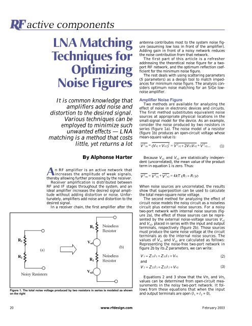
active components<strong>LNA</strong> <strong>Matching</strong><strong>Techniques</strong> <strong>for</strong><strong>Optimizing</strong><strong>Noise</strong> <strong>Figures</strong>It is common knowledge thatamplifiers add noise anddistortion to the desired signal.Various techniques can beemployed to minimize suchunwanted effects — <strong>LNA</strong>matching is a method that costslittle, yet returns a lotantenna contributes most to the system noise figure(assuming low loss in front of the amplifier).Adding gain in front of a noisy network reducesthe noise contribution from that network.The first part of this article is a refresheraddressing the theoretical noise figure <strong>for</strong> a twoportRF network, and the optimum reflection coefficient<strong>for</strong> the minimum noise figure.The rest deals with using scattering parameters(S parameters) as a design tool to match impedances<strong>for</strong> minimum noise figure. The analysis considersoptimum noise matching <strong>for</strong> an SiGe lownoiseamplifier.Amplifier <strong>Noise</strong> FigureTwo methods are available <strong>for</strong> analyzing theeffect of noise in electronic devices and circuits.The first method substitutes equivalent noisesources at appropriate physical locations in thesmall-signal model <strong>for</strong> the device. As an example,consider the noise produced by two resistors inseries (figure 1a). The noise model of a resistor(figure 1b) produces an open-circuit voltage whosemean-square value is:2 2V no= 2( V n 1+V n 2) = V n + V n V n +2 1 2 1 2 V n2...(1)By Alphonse HarterAn RF amplifier is an active network thatincreases the amplitude of weak signals,thereby allowing further processing by the receiver.Receiver amplification is distributed betweenRF and IF stages throughout the system, and anideal amplifier increases the desired signal amplitudewithout adding distortion or noise. Un<strong>for</strong>tunately,amplifiers add noise and distortion to thedesired signal.In a receiver chain, the first amplifier after theBecause V n1 and V n2 are statistically independent(uncorrelated), the mean value of the productterm in equation 1 is zero. Thus:2V no= 2V n+ 2 1 V n2= 4kT ( R1+R2)bWhen noise sources are uncorrelated, the resultsshow that superposition can be used to calculatethe total mean-square noise voltage.The second method <strong>for</strong> analyzing the effect ofcircuit noise models the noisy circuit as a noiselesscircuit plus external noise sources. For a noisytwo-port network with internal noise sources (figure2a), the effect of those sources can be representedby the external noise-voltage sources V n1and V n2 , placed in series with the input and outputterminals, respectively (figure 2b). Those sourcesmust produce the same noise voltage at the circuitterminals as do the internal noise sources. Thevalues of V n1 and V n2 are calculated as follows:Representing the noise-free two-port network infigure 2b by its Z parameters, we can write:V = Z I + Z I + V1 11 1 12 2 n1andV = Z I + Z I + V2 21 1 22 2 n2(2)(3)Figure 1. The total noise voltage produced by two resistors in series is modeled as shownon the rightEquations 2 and 3 show that the Vn 1 and Vn 2values can be determined from open-circuit measurementsin the noisy two-port network. It followsfrom these equations that when the inputand output terminals are open (I 1 = I 2 = 0),20 www.rfdesign.com February 2003
Figure 2. A noisy two-port network (a) can be modeled by a noise-free two-port network (b) with externalnoise-voltage sources V n1 and V n2Vn1 = V1|I1 = I2= 0andVn2 = V2|I1 = I2= 0In other words, V n1 and V n2 equal thecorresponding open-circuit voltages.In an alternate representation of thenoisy two-port network (figure 3), theexternal sources are the current-noisesources I n1 and I n2 . Representing thenoise-free two-port network, we canwrite:I1 = Y11I1+ Y12I2+In1andI2 = Y21I1+ Y22I2+In2The values of I n1 and I n2 in figure 3 followfrom short-circuit measurementstaken in the noisy two-port network.That is:1 s ysys= − Γ 1 −↔ Γ11 + Γs1 + ysand1 opt yyopt= − Γ 1 −↔ Γ11 + Γopt1 + yBesides that of figures 2b and 3,other representations can be derived<strong>for</strong> a noisy two-port. A representationconvenient <strong>for</strong> noise analysis places thenoise source at the input of the network(figure 4). Representing the noise-freetwo-port network in figure 4 by itsABCD parameters, it can be written:optoptFigure 3. A noisy two-port network can also berepresented by a noise-free two-port with externalnoise-current sources I n1 and I n2figure 2b is derived from the following.Using Z parameters to represent thenoise-free two-port network in figure 4,it can be written:V1 = Z11( I1−In)+ Z12I2+Vn= Z11I1 + Z12I2 + ( Vn−Z11In)andV = Z ( I − In)+Z I= Z21I1 + Z22I2 −Z21In2 21 1 22 2(4)(5)Comparing (2) and (3) with (4) and (5),it follows that:Vn1 = Vn−Z11In(6)Vn2 = Vn2−Z21In(7)Hence, solving (6) and (7) <strong>for</strong> V n and I ngives:ZV = V − ⎛ V⎝ ⎜ 11⎞1Z ⎠⎟21andn n n2VnIn =− ⎛ ⎝ ⎜ 2⎞Z ⎠⎟21A source connected to the noisy twoportnetwork (see figure 5) is representedby a current source with admittanceY s . It is assumed that noise from thesource is uncorrelated with noise fromthe two-port network. Thus, noise poweris proportional to the mean square of theshort-circuit current (denoted by I 2 SC) atthe input port of the noise-free amplifier,and noise power due to the source aloneis proportional to the mean square of thesource current (I 2 S ). Hence, the noisefigure F is given by:FI 2=2ISCS(10)Because I sc = –I s + I n + V n Y s , it followsthat the mean square of I sc is given by:2 2I SC = ( − Is + In + VnYs)= I S+ ( In+VY n s) − 2Is( In+VY n s)2 2(11)And, because noise from the source andnoise from the two-port network areuncorrelated, we have:2I S( In+VnYs) = 02Equation 2I I11 reducesI Vto:SC =2S + ( n + nYs)Substituting (12) into (10) gives:(12)( In+VnYs)F = 1 +(13)2I SThere is some correlation between theexternal sources V n and I n . Hence, I ncan be written as the sum of two terms,one uncorrelated to V n (I un ) and one correlatedto V n (I nc ). Thus:In = Inu+Inc2(14)V1 = AV2+ B( −I2)+VandI1 = CV2+ D( −I2)+IThe previous equations show there isno simple way to evaluate V n and I n in figure4 using open- and short-circuit measurements.From a practical point of view,those values (V n and I n ) can be expressedin terms of the noise voltages V n1 and V n2in figure 2b (which require only open-circuitmeasurements). The relationshipbetween noise sources V n and I n in figure4 and noise sources V n1 and V n2 innnAn alternate method <strong>for</strong> determiningV n and I n relates them to the noisesources I n1 and I n2 in figure 3. In thiscase the relationships are:InVn=− ⎛ ⎝ ⎜ 2 ⎞Y ⎠⎟21andYI = I − ⎛ I⎝ ⎜ 11⎞1Y ⎠⎟21n n n2(8)(9)Furthermore, defining the relationbetween I nc and V n in terms of a correlationadmittance, Y c, gives:I= Y Vnc c c(15)However, Y C is not an actual admittancein the circuit. It is defined by (15)and calculated as follows:From (14):In = Inu+YcVc(16)Multiplying (16) by V* n , taking the24 www.rfdesign.com February 2003
Figure 4. A noisy two-port network can be representedas a noise-free two-port with externalnoise sources V n and I n at the inputmean, and observing that:InuVn * = 0 , we obtain:V∗nInIV n n∗ =2YV c n, or Yc =2V nSubstituting (16) into (13) produces thefollowing expression <strong>for</strong> F:( Inu + ( Yc + Ys)Vn)F = 1 +(17)2I s<strong>Noise</strong> produced by the source isrelated to the source conductance by:I(18)where G s = R e [Y s ]. The noise voltagecan be expressed in terms of an equivalentnoise resistance R n as:(19)The uncorrelated noise current can beexpressed in terms of an equivalentnoise conductance, G u , namely:I(20)Substituting (18), (19), and (20) into(17), and letting Y c = G c + jB c and Y s =G s + jB s gives:F2sV2n2n1= 4kT0GsB== 4kT0RnB= 4kT0GuB4kT0GuB + Gs+ jBs+ Gc+jBc 4kT0RnB(21)4kT0GsBGuRn= 1 + + ⎡( G G G s+G c) 2 + ( + )2 ⎤s s⎣BsBc⎦The noise factor can be minimized byproperly selecting Y S . From (21), F isdecreased by selecting B S = –B C. (22)Hence, from (21):GuRnF B(23)G G G G2=− BS c = 1 + + ( s+c)s sThe dependence of the expression in(23) on G s can be minimized by setting:FBS=−Bc= 0dGs22Figure 5. This noise model lets you calculatethe amplifier noise figureWhich gives:FBS =−BC Guwhich gives: =−2dGs G SR G S G S G C G S G2( 2 ( + )−( + C))+ n= 02G SSolving <strong>for</strong> G S , we obtain:G(24)The values of G S and B S in (24) and(22) give the source admittance, whichresults in the minimum (optimum)noise figure. This optimum value of thesource admittance is commonly denotedby Y opt = G opt + jB opt . This is given as:GuYopt = Gopt + Bopt= G 2 C+ − jBRn(25)From (23), The minimum noise figure,F min , is:FsG= G 2 c +RGuRnF Y s(26)G G G G2= = 1 + + ( opt + c)opt optmin |unSolving (24) <strong>for</strong> G U /G opt and substitutinginto (26) gives: 2⎛ G C⎞GuFmin = 1 + RnGopt−⎝⎜Gopt⎠⎟GoptRn(27)G G 2+ ( opt + 2 G opt G c + G 2 c)opt= 1+ 2Rn( Gopt+Gc)Using (27), we can write (21) as:GuF = Fmin − 2Rn( Gopt+Gc)+GsRnG G s G 2+ ⎡( + c) + ( B s−B2opt)⎤s⎣⎦(28)Solving Equation 24 <strong>for</strong> G U and substitutinginto (28), the expression <strong>for</strong> Fcan be simplified to:F = FminRnG G G 2+ ( s−opt) + ( B s−B2⎡opt)⎤s⎣⎦c(29)Equation 29 shows that F dependson Y opt = G opt + jB opt , and on F min . Whenthese quantities are specified, the valueof F can be determined <strong>for</strong> any sourceadmittance, Y s . This equation can alsobe expressed as:rnF Fg y y 2= min + s− opt = Fsrn2+ ys−yoptReal( ys)(30)where r n = R n /Z 0 is the normalizednoise resistance. And y s = Y S Z 0 is thenormalized source admittance. Hence:Yand y opt is the normalized value of theoptimum source admittance:YsY G + jB= =Y 0 Yoopts s sY G= =Y+ jBYopt opt opt0 0= gs+jbmin= gopt+ jbAdmittances y S and y opt can beexpressed in terms of reflection coefficients:1 s ysys= − Γ 1 −↔ Γ11 + Γs1 + ysand1 opt yoptyopt= − Γ 1 −↔ Γ11 + Γopt1 + yoptExpressing y S and y opt in terms ofreflection coefficients help <strong>for</strong>mulatethe noise figure (NF) of (30) as a functionof those coefficients. This <strong>for</strong>mulationis more convenient <strong>for</strong> industrial<strong>LNA</strong> applications, because in most datasheets the <strong>LNA</strong> characteristics areexpressed as a table of S parametersand the optimum reflection coefficientΓ opt versus frequency, as:2Γs−ΓoptF = F min+4rn(31)2 21+ Γopt( 1−Γs)When the noise figure {F in (31)} isexpressed as a function of a circle, itcan be used with a Smith chart <strong>for</strong> optimumnoise-figure matching in specificapplications as show in the followingset of equations.sopt26 www.rfdesign.com February 2003
F − F min Γs−Γopt=2 24rn1+ Γopt( 1−Γs);F − F4rnF − FN=4rnN=and( 1+N) Γ = N + 2Γ Γ − ΓandΓΓ2s2smin212+ Γopt=2optΓs−ΓN= with2( 1 − Γs)min1 +ΓΓs− 2Γ Γ + Γ( 1 − Gs)N( 1−Γ )= Γ − 2Γ Γ + Γ2 2s s opt optN 2=( 1 + ) + ΓΓ s optN ( 1+N) − Γopt1+N;2ΓΓ s opt Γopt Γopt−22( 1 + N) + ( 1+N) − ( 1+N)ΓoptNΓs−( 1+N) = ( 1+N)2 2optoptΓ Γ−( + N) + 21 ( 1 + N)22s opt opt2opt2optN Γ=( 1+N) − ( 1+N)2Γs−Γ2 2 2s s s opt opt22;2opt2( 1 − Γs)2;2;;ΓoptON= , with( 1 + N)N= F − F min1 + Γ4rnRadius:RN2opt1=N N 2 N2+ − opt( 1 + )( 1 Γ )Designing <strong>for</strong> Optimum <strong>Noise</strong> FigureFor any two-port network, the noisefigure gives a measure of the amount ofnoise added to a signal transmittedthrough the network. For any practicalcircuit, the signal-to-noise ratio at itsoutput will be worse (smaller) than atits input. In most circuit designs, however,you can minimize the noise contributionof each two-port networkthrough a judicious choice of operatingpoint and source resistance.The preceding section demonstratesthat <strong>for</strong> each <strong>LNA</strong> (indeed, <strong>for</strong> any twoportnetwork) there exists an optimumnoise figure. <strong>LNA</strong> manufacturers oftenspecify an optimum source resistanceon the data sheet.To design an amplifier <strong>for</strong> minimumnoise figure, determine (experimentallyor from the data sheet) the source resistanceand bias point that produce theminimum noise figure <strong>for</strong> that device.Next, <strong>for</strong>ce the actual source impedanceto “look like” that optimum value. Allstability considerations still apply, ofcourse. If the calculated Rollet stabilityfactor (K) is less than 1 (K is defined inthe literature as a figure of merit <strong>for</strong><strong>LNA</strong> stability), then the source andload-reflection coefficients must becarefully chosen. For an accurategraphical depiction of the unstableregions, it is best in that case to drawstability circles.After providing the <strong>LNA</strong> with optimumsource impedance, the next stepis to determine the optimum loadreflectioncoefficient (ΓL) needed toproperly terminate the <strong>LNA</strong>'s output:⎡ ΓSΓLS S 21 S 12 ⎤= 22⎣⎢ − S ΓS⎦⎥ *1 11where Γ S is the source-reflection coefficientnecessary <strong>for</strong> minimum noise figure.(The asterisk in the above equationindicates the conjugate of the complexquantity Γ L .)ApplicationsFor practical examples to supportthe theory of optimum noise matching<strong>for</strong> <strong>LNA</strong>s, we examine an <strong>LNA</strong> (figure6) with high third-order adjustableintercept point (IP3). This particulardesign is <strong>for</strong> personal communicationssystem (PCS) phone applications withgain selected by logic control (14.5 dBin high-gain mode and 0.8 dB in lowgainmode), the amplifier exhibits anoptimum noise figure of 1.9 dB(depending on the value of bias resistor,R bias ).The figure 6 application employs an<strong>LNA</strong> operating at a PCS receiver frequencyof 1960 MHz and noise figure of2 dB. It must operate between 50Ω terminations.For this particular device,the optimum R bias <strong>for</strong> minimum noisefigure is 715Ω. The optimum sourcereflectioncoefficient Γ OPT <strong>for</strong> minimumnoise figure in a 1960 MHz applicationΓoptΓs−( 1 + N)2N= ⎡ΓoptN N 2+( + )N2( 1 −⎣ )⎤21⎦.For <strong>LNA</strong> input matching, a noise circleis positioned on the Smith chart’scenter and radius.Center:Figure 6.Typical operating circuit <strong>for</strong> the referenced <strong>LNA</strong>28 www.rfdesign.com February 2003
Figure 7. The solid circle on this Smith chart depicts the desired (optimum)2dB noise figure <strong>for</strong> the PCS <strong>LNA</strong> with input matchingFigure 8.figureThe <strong>LNA</strong> with output matching <strong>for</strong> a desired (optimum) 2dB noise(F MIN = 1.79 dB) is:Γopt = 0. 130 / 124. 48oA source impedance with noise-equivalentresistance R N = 43.2336Ω yieldsthe minimum noise figure.This particular <strong>LNA</strong> operating at1960 MHz has the following S parameters(expressed as magnitude/angle):S 11 = 0.588/–118.67°S 21 = 4.12/149.05°S 12 = 0.03/–167.86°S 22 = 0.275/–66.353°The calculated stability factor (K =2.684) indicates unconditional stability,so we can proceed with the design.Figure 6 (a typical operating circuit)shows design values <strong>for</strong> the inputmatching network. First, a Smith chart<strong>for</strong> input matching shows (in blue) the2 dB constant-noise circle requested bydesign (figure 7). For comparison, notethe dotted-line depiction of constantnoisecircles corresponding to noise figuresof 2.5 dB, 3 dB, and 3.5 dB.For convenience, we choose a sourcereflectioncoefficient of Γ S = 0.3/150° onthe 2 dB constant-noise circle. The normalized50Ω source resistance is trans<strong>for</strong>medto Γ S using three components:The arc Γ SA (clockwise in the impedancechart) gives the value of series inductanceL 1 . Arc B O (clockwise in theadmittance chart) gives the value ofshunt capacitor C 1 .The value of arc Γ SA measured on theplot is 0.3 units, so Z = 50(0.3) = 15Ω.Thus, L 1 = 15/ω = 15/(2πf) = 15/(2π)(1.96x 10 9 ) = 1.218 nH, rounded to 1.2 nH.Value of the arc B O measured on theplot is 0.9 units, so 1/Y = Z = 50/0.9 =55.55Ω. Thus, C 2 = 1/(55.55(ω)) =1/(55.55(2pf)) = 1/(55.55)(2π)(1.96 x 10 9 )= 1.46 pF, rounded to 1.5 pF.Capacitor C 1 is just a high-valuedDC isolation capacitor, and does notinterfere with the input matching. Thechosen Γ S provides the load-reflectioncoefficient needed to properly terminatethe <strong>LNA</strong>:⎡ ΓSΓLS S 21 S 12 ⎤= 22⎣⎢ − S ΓS⎦⎥ * = 0. 236 / 70. 5o1 11This value and the normalized loadresistancevalue are plotted in Figure 8,which also shows a possible method <strong>for</strong>trans<strong>for</strong>ming the 50Ω load into Γ L . Forthis example, note that a single seriescapacitor provides the necessaryimpedance trans<strong>for</strong>mation.The arc OΓ L (counterclockwise in theimpedance chart) gives the value <strong>for</strong>series capacitor C 3 . The value of arcOΓ L measured on the plot is 0.45 units,so Z = 50(0.45) = 22.5Ω. Thus, C 3 =1/(22.5(ω)) = 1/(22.5)(2πf)) =1/(22.5)(2π)(1.96 x 10 9 ) = 3.608 pF,rounded to 3.6pF.References1. Guillermo Gonzalez, MicrowaveTransistor Amplifiers, Analysis &Design, 2nd ed. (Upper Saddle River,New Jersey: Prentice Hall, 1996) .2. Christopher Bowick, RF CircuitDesign, (Newnes, 1997).About the authorAlphonse Harter is the corporatefield application engineer <strong>for</strong>Maxim Integrated Products Inc.(www.maxim-ic.com) in the Franceoffice. He covers the southern Europeregion <strong>for</strong> the wireless productsgroup. He may be reached atalphonse_harter@maximhq.com.30 www.rfdesign.com February 2003