High power RF-LDMOS transistors for base station applications
High power RF-LDMOS transistors for base station applications
High power RF-LDMOS transistors for base station applications

You also want an ePaper? Increase the reach of your titles
YUMPU automatically turns print PDFs into web optimized ePapers that Google loves.
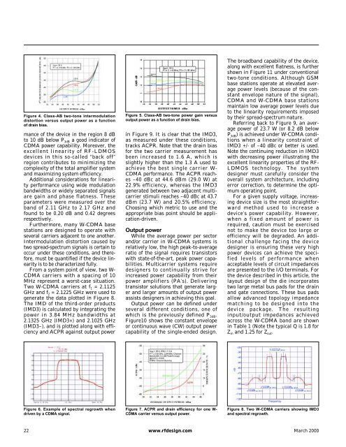
Figure 4. Class-AB two-tone intermodulation<br />
distortion versus output <strong>power</strong> as a function<br />
of drain bias.<br />
mance of the device in the region 8 dB<br />
to 10 dB below P 3dB a good indicator of<br />
CDMA <strong>power</strong> capability. Moreover, the<br />
excellent linearity of <strong>RF</strong>-<strong>LDMOS</strong><br />
devices in this so-called “back off”<br />
region contributes to minimizing the<br />
complexity of the total amplifier system<br />
and maximizing system efficiency.<br />
Additional considerations <strong>for</strong> linearity<br />
per<strong>for</strong>mance using wide modulation<br />
bandwidths or widely separated signals<br />
are gain and phase flatness. These<br />
parameters were measured over the<br />
band of 2.11 GHz to 2.17 GHz and<br />
found to be 0.20 dB and 0.42 degrees<br />
respectively.<br />
Furthermore, many W-CDMA <strong>base</strong><br />
<strong>station</strong>s are designed to operate with<br />
several carriers adjacent to one another.<br />
Intermodulation distortion caused by<br />
two spread-spectrum signals is certain to<br />
occur under these conditions, and there<strong>for</strong>e,<br />
must be quantified if the device linearity<br />
is to be characterized fully.<br />
From a system point of view, two W-<br />
CDMA carriers with a spacing of 10<br />
MHz represent a worst-case situation.<br />
Two W-CDMA carriers at f 1 = 2.1125<br />
GHz and f 2 = 2.1225 GHz were used to<br />
generate the data plotted in Figure 8.<br />
The IMD of the third-order products<br />
(IMD3) is calculated by integrating the<br />
<strong>power</strong> in 3.84 MHz bandwidths at<br />
2.1325 GHz (IMD3+) and 2.1025 GHz<br />
(IMD3–), and is plotted along with efficiency<br />
and ACPR against output <strong>power</strong><br />
Figure 5. Class-AB two-tone <strong>power</strong> gain versus<br />
output <strong>power</strong> as a function of drain bias.<br />
in Figure 9. It is clear that the IMD3,<br />
as measured under these conditions,<br />
tracks ACPR. Note that the drain bias<br />
<strong>for</strong> the two carrier measurement has<br />
been increased to 1.6 A, which is<br />
slightly higher than the 1.3 A used to<br />
achieve the best single carrier W-<br />
CDMA per<strong>for</strong>mance. The ACPR reaches<br />
–40 dBc at 44.6 dBm (29.0 W) at<br />
22.9% efficiency, whereas the IMD3<br />
generated between two adjacent multicarrier<br />
stimuli reaches –40 dBc at 43.7<br />
dBm (23.7 W) and 20.5% efficiency.<br />
Choosing which metric to use and the<br />
appropriate bias point should be application-driven.<br />
Output <strong>power</strong><br />
While the average <strong>power</strong> per sector<br />
and/or carrier in W-CDMA systems is<br />
relatively low, the high peak-to-average<br />
ratio of the signal requires <strong>transistors</strong><br />
with state-of-the-art, peak <strong>power</strong> capabilities.<br />
Multicarrier systems require<br />
designers to continually strive <strong>for</strong><br />
increased <strong>power</strong> capability from their<br />
<strong>power</strong> amplifiers (PA’s). Delivering<br />
transistor solutions that generate larger<br />
and larger amounts of output <strong>power</strong><br />
assists designers in achieving this goal.<br />
Output <strong>power</strong> can be defined under<br />
several different conditions, one of<br />
which is the previously defined P 3dB .<br />
Figure10 shows the constant envelope<br />
or continuous wave (CW) output <strong>power</strong><br />
capability of the single-ended design.<br />
The broadband capability of the device,<br />
along with excellent flatness, is further<br />
shown in Figure 11 under conventional<br />
two-tone conditions. Although GSM<br />
<strong>base</strong> <strong>station</strong>s operate at elevated average<br />
<strong>power</strong> levels (because of the constant<br />
envelope nature of the signal),<br />
CDMA and W-CDMA <strong>base</strong> <strong>station</strong>s<br />
maintain low average <strong>power</strong> levels due<br />
to the linearity requirements imposed<br />
by their spread-spectrum nature.<br />
Referring back to Figure 9, an average<br />
<strong>power</strong> of 23.7 W (or 8.2 dB below<br />
P 3dB ) is achieved under W-CDMA conditions<br />
when a linearity constraint of<br />
IMD3 +/- of –40 dBc or better is used.<br />
Note the continuing reduction in IMD3<br />
with decreasing <strong>power</strong> illustrating the<br />
excellent linearity properties of the <strong>RF</strong>-<br />
<strong>LDMOS</strong> technology. The system<br />
designer must carefully consider the<br />
overall system architecture, including<br />
error correction, to determine the optimum<br />
operating point.<br />
For a given supply voltage, increasing<br />
device size is the most straight<strong>for</strong>ward<br />
method used to increase a<br />
device’s <strong>power</strong> capability. However,<br />
when a fixed amount of <strong>power</strong> is<br />
required, caution must be exercised<br />
not to make the device too large or<br />
efficiency will be degraded. An additional<br />
challenge facing the device<br />
designer is ensuring these very high<br />
<strong>power</strong> devices can achieve the specified<br />
levels of per<strong>for</strong>mance when<br />
acceptable levels of circuit impedances<br />
are presented to the I/O terminals. For<br />
the device described in this article, the<br />
layout design of the die incorporates<br />
two large metal bus pads <strong>for</strong> the drain<br />
and gate connections. These bus pads<br />
allow advanced topology impedance<br />
matching to be designed into the<br />
device package. The resulting<br />
input/output impedances achieved<br />
across the W-CDMA band are shown<br />
in Table 1 (Note the typical Q is 1.8 <strong>for</strong><br />
Z in and 1.25 <strong>for</strong> Z out .<br />
Figure 6. Example of spectral regrowth when<br />
driven by a CDMA signal.<br />
Figure 7. ACPR and drain efficiency <strong>for</strong> one W-<br />
CDMA carrier versus output <strong>power</strong>.<br />
Figure 8. Two W-CDMA carriers showing IMD3<br />
and spectral regrowth.<br />
22 www.rfdesign.com March 2000